Table of Contents
- 1. Product Overview
- 1.1 Core Advantages and Target Market
- 2. In-depth Analysis of Technical Parameters
- 2.1 Absolute Maximum Ratings
- 2.2 Electro-Optical Characteristics
- 2.2.1 Input Characteristics
- 2.2.2 Output Characteristics
- 2.2.3 Transmission Characteristics
- 3. Grading System Description
- 4. Performance Curve Analysis
- 5. Mechanical and Packaging Information
- 5.1 Package Dimensions and Type
- 5.2 Pad Layout and Polarity Marking
- 6. Soldering and Assembly Guidelines
- 7. Packaging and Ordering Information
- 8. Application Suggestions
- 8.1 Typical Application Circuit
- 8.2 Design Considerations
- 9. Technical Comparison and Differentiation
- 10. Frequently Asked Questions (Based on Technical Parameters)
- 11. Practical Design Case Study
- 12. Working Principle
- 13. Technology Trends
1. Product Overview
The H11AAX series is a family of AC input optocouplers (also known as opto-isolators or photocouplers). These devices are specifically designed to provide electrical isolation between AC or unknown polarity DC input circuits and output control circuits. Their core function is to transmit electrical signals using light, thereby eliminating electrical connections and preventing ground loops, voltage spikes, and noise from propagating between circuits.
This series includes four main models: H11AA1, H11AA2, H11AA3, and H11AA4. The primary difference between them lies in the Current Transfer Ratio (CTR), which defines the signal transmission efficiency from the input to the output. These devices utilize a compact 6-pin Dual In-line Package (DIP), offering standard through-hole mounting, wide pin spacing, and Surface Mount Device (SMD) options.
1.1 Core Advantages and Target Market
The H11AAX series offers several key advantages, making it suitable for demanding industrial and consumer applications. Its most prominent feature is an isolation voltage of up to 5000Vrms, which is crucial for the safety and reliability of mains-connected equipment. A creepage distance exceeding 7.62mm further enhances its safety rating. The device is certified by major international safety agencies including UL, cUL, VDE, SEMKO, NEMKO, DEMKO, FIMKO, and CQC, making it globally suitable for products requiring regulatory compliance.
The integrated back-to-back infrared LED configuration at the input is its signature feature. This design allows the device to be driven directly by AC voltage or DC voltage of unknown polarity without the need for an external rectification circuit, thereby simplifying circuit design. The output is a silicon NPN phototransistor.
The target markets and applications are diverse, primarily focusing on areas where electrical isolation and AC signal detection are crucial. Typical applications include AC line monitoring for detecting the presence of mains voltage, telephone line interface circuits, and sensors in industrial control systems for detecting DC signals of unknown polarity.
2. In-depth Analysis of Technical Parameters
This section provides a detailed and objective analysis of the electrical, optical, and thermal characteristics specified in the datasheet. Understanding these parameters is crucial for reliable circuit design.
2.1 Absolute Maximum Ratings
These ratings define the stress limits of the device. Operation beyond these limits may cause permanent damage. Operation under these conditions is not guaranteed.
- Ifiweranṣẹ iwọle (IF):60 mA (tẹsiwaju). Eyi ni ifiweranṣẹ DC ti o pọ julọ ti o le fi sii si LED iwọle.
- Ifiweranṣẹ iwọle oke (IFM):It is 1 A for an extremely short pulse duration of 10 µs. This rating is very important for withstanding transient surges.
- Input Power Dissipation (PD):It is 120 mW at an ambient temperature of 25°C, derating at a rate of 3.8 mW/°C above 90°C. This limits the product of VF * IF.
- Output Collector-Emitter Voltage (VCEO):80 V. The maximum voltage that can be sustained between the collector and emitter of the phototransistor when the base is open.
- Device Total Power Dissipation (PTOT):200 mW. Ba a haɗa ƙarfin shigarwa da na fitarwa ba su wuce wannan ƙimar ba.
- Ƙarfin keɓancewa (VISO):A cikin zafi na 40-60%, 5000 Vrms na tsawon minti 1. Wannan muhimmin sigar aminci ne, lokacin gwajin ana taƙaita hanyoyin shigarwa da fitarwa daban.
- Zafin aiki (TOPR):-55°C to +100°C. The device operates normally over this full industrial temperature range.
- Soldering Temperature (TSOL):260°C for up to 10 seconds, suitable for wave soldering or reflow soldering processes.
2.2 Electro-Optical Characteristics
These parameters are typically measured at 25°C and define the device's performance under normal operating conditions.
2.2.1 Input Characteristics
- Forward Voltage (VF):Typical value 1.2V, maximum 1.5V at a forward current (IF) of ±10mA. The symmetrical value indicates the behavior of the reverse-parallel LED pair.
- Input Capacitance (Cin):Typical value 80 pF. This may affect the high-frequency performance of the driving circuit.
2.2.2 Output Characteristics
- Collector-Emitter Dark Current (ICEO):Maximum 50 nA at VCE=10V and IF=0mA. This is the leakage current of the phototransistor in the absence of light, important for off-state leakage.
- Breakdown Voltage (BVCEO, BVCBO, BVECO):Minimum values are 80V, 80V, and 7V respectively. These define the withstand voltage capability under different pin configurations.
- Collector-Emitter Saturation Voltage (VCE(sat)):Maximum 0.4V at IF=±10mA and IC=0.5mA. This is the voltage drop across the output transistor when it is fully turned on.
2.2.3 Transmission Characteristics
These parameters define the signal transmission efficiency and speed.
- Current Transfer Ratio (CTR):This is the core grading parameter of the series, defined as (IC / IF) * 100% under specific conditions (IF=±10mA, VCE=10V).
- H11AA1: CTR ≥ 20%
- H11AA2: CTR ≥ 10%
- H11AA3: CTR ≥ 50%
- H11AA4: CTR ≥ 100%
- CTR Symmetry:The ratio of the CTR of one LED polarity to the CTR of the other polarity, specified to be between 0.5 and 2.0. This indicates the balance level of two anti-parallel LEDs.
- Isolation Resistance (RIO):Minimum 10^11 Ω at 500 V DC. This is the DC resistance between input and output, contributing to isolation quality.
- Input-Output Capacitance (CIO):Typical value 0.7 pF. This extremely low capacitance is crucial for suppressing high-frequency common-mode noise across the isolation barrier.
- Switching Times (Ton, Toff, Tr, Tf):Under test conditions (VCC=10V, IC=10mA, RL=100Ω), the maximum value for all parameters is 10 µs. These times define the output's response speed to input signal changes, limiting the maximum AC frequency or data rate.
3. Grading System Description
The H11AAX series employs a simple grading system based solely on Current Transfer Ratio (CTR).
CTR Grading (X in H11AAX):The numerical suffix (1, 2, 3, 4) directly corresponds to the minimum guaranteed CTR percentage listed in Section 2.2.3. There is no grading based on wavelength, forward voltage, or other parameters. Designers must select the appropriate grade based on the required output current drive capability versus the available input current. For example, the H11AA4 (minimum CTR 100%) has the highest sensitivity and is suitable for applications with very low input drive capability; whereas in circuits with higher available drive current, the H11AA2 may be sufficient and more cost-effective.
4. Performance Curve Analysis
Datasheet ya yi nuni da madaidaicin layukan halayen haske da lantarki. Ko da yake ba a kwafin takamaiman zane-zane a cikin rubutun da aka bayar, amma manufarsu da bayanan da suke isarwa sun zama daidai ga irin wannan kayan aiki.
Madaidaicin layukan sun haɗa da:
- The relationship between Current Transfer Ratio (CTR) and Forward Current (IF):This curve shows how CTR varies with drive current. Typically, CTR is highest at moderate IF and may decrease at very low or very high currents.
- The relationship between CTR and Ambient Temperature (Ta):CTR ya optocoupler koyaushe yana da coefficient mara kyau na zafin jiki, wanda ke nufin yana raguwa yayin da zafin jiki ya karu. Wannan jadawali yana da mahimmanci don ƙirƙirar da'ira mai aiki a cikin kewayon zafin jiki gaba ɗaya.
- Dangantakar ƙarar mai tara (IC) da ƙarfin lantarki mai tara-mai fitarwa (VCE):Wannan shine dangin lanƙwan halayen fitarwa, mai kama da transistor bipolar, tare da ƙarar LED shigar (IF) a matsayin siga. Yana nuna yankin jikewa da yankin aiki.
- Dangantakar ƙarfin lantarki na gaba (VF) da ƙarar gaba (IF):Input the IV characteristics of the LED pair.
- Relationship between switching time and load resistance (RL):Show how rise, fall, turn-on, and turn-off times are affected by the output load.
Designers should consult these curves in the complete datasheet to understand nonlinear behaviors and derating factors not reflected in the min/typ/max tables.
5. Mechanical and Packaging Information
The device is offered in multiple package variants to accommodate different assembly processes.
5.1 Package Dimensions and Type
- Standard DIP Type:Default through-hole package.
- M-type option:Features "wide pin bend," providing a pin pitch of 0.4 inches (approximately 10.16mm) instead of the standard 0.3 inches (7.62mm), suitable for circuit boards requiring greater creepage distance.
- S-type option:Surface mount pin form for reflow soldering.
- S1-type option:A "low-profile" surface mount version, possibly with a lower PCB mounting height.
Detailed dimension drawings are provided for each type, including body dimensions, lead length, lead pitch, and coplanarity specifications. These are crucial for PCB pad design.
5.2 Pad Layout and Polarity Marking
Recommended pad layouts are provided for the surface mount options (S and S1). The datasheet notes that this is a recommendation, and designers should modify it based on their specific PCB fabrication process and thermal requirements.
Device marking:The top of the package is marked with:
- "EL" (manufacturer code)
- Full model number (e.g., H11AA1)
- 1-digit year code (Y)
- 2-digit week code (WW)
- Optional "V" suffix if the unit is specified for VDE safety certification.
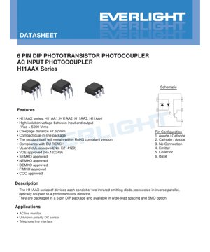
Pin configuration (6-pin DIP):
1. Anode/Cathode (LED1 Anode, LED2 Cathode)
2. Cathode/Anode (LED1 Cathode, LED2 Anode)
3. No Connection (NC)
4. Emitter (Phototransistor)
5. Collector (Phototransistor)
6. Base (Phototransistor). The base pin is typically left floating or connected to the emitter via a resistor for sensitivity adjustment or speed enhancement.
6. Soldering and Assembly Guidelines
A key guideline in the Absolute Maximum Ratings is the soldering temperature: 260°C for a maximum of 10 seconds. This is compatible with standard lead-free (SnAgCu) reflow profiles.
Important Notice:
- Moisture Sensitivity:Although not explicitly stated in the provided text, plastic-encapsulated SMD optocouplers typically have a Moisture Sensitivity Level (MSL). For surface-mount components (S, S1 options), the manufacturer's handling instructions regarding baking and floor life must be followed to prevent "popcorning" during the reflow soldering process.
- Cleaning:Ensure the cleaning solvent is compatible with the plastic material of the device.
- Storage Conditions:According to the datasheet, the storage temperature range is -55°C to +125°C. The device should be stored in a dry, anti-static environment.
7. Packaging and Ordering Information
Ordering codes follow the pattern below:H11AAXY(Z)-V
- X:CTR Level (1, 2, 3, 4).
- Y:Pin Form Option.
- None: Standard DIP-6 (65 pcs/tube).
- M: Wide lead bend (65 pcs/tube).
- S: Surface mount lead form.
- S1: Thin surface mount pin form.
- Z:Tape and reel options (for S/S1 only).
- TA: Specific reel and reel types.
- TB: Alternative reel and reel types.
- Both TA and TB are 1000 units per reel.
- V:Optional VDE safety certification mark.
Tape and reel specifications:Provides detailed dimensions for carrier tape (pocket size A, B), cover tape, and reels for automated surface mount assembly.
8. Application Suggestions
8.1 Typical Application Circuit
AC Line Monitor:The input is directly connected across the AC line (with a current-limiting resistor). The output transistor switches synchronously with the AC zero-crossing, providing a digital pulse train or rectified signal to the microcontroller for detecting the presence of the power supply.
Unknown Polarity DC Sensor:Reverse parallel input allows the device to be connected to a DC voltage source without considering polarity, making it ideal for detection in battery-powered devices or industrial sensors where wiring polarity may be reversed.
Telephone Line Interface:Used for ring detection or off-hook detection, providing isolation between the telephone line and logic circuits.
8.2 Design Considerations
- Input Current Limitation:A series resistor must always be used to limit the input current (IF) to a safe value below 60mA, calculated based on the peak input voltage and the LED forward voltage. The power rating of the resistor must also be considered.
- Output Load:The load resistor (RL) on the collector determines the output voltage swing and affects the switching speed. A smaller RL provides faster switching speed but consumes more power.
- Noise Immunity:Low input-output capacitance (0.7pF) provides excellent high-frequency common-mode noise rejection. For optimal performance, physically separate the input and output traces on the PCB.
- CTR Degradation:Over extended periods and at high temperatures, the CTR of an optocoupler may degrade. For critical long-life applications, design with sufficient initial CTR margin.
9. Technical Comparison and Differentiation
The H11AAX series primarily differentiates itself through itsAC input capability(achieved via a back-to-back LED structure). Most standard optocouplers (e.g., 4N25, PC817) have a single LED input requiring a defined forward bias, thus necessitating an external bridge rectifier for AC operation. The H11AAX integrates this functionality.
Compared to other communication input optocouplers, its main advantage isIsolation rating up to 5000Vrmsandcomprehensive international safety certifications(UL, VDE, etc.), which are crucial for products sold in multiple global markets. The availability of multiple CTR grades and package types (through-hole and SMD) provides design flexibility.
10. Frequently Asked Questions (Based on Technical Parameters)
Q1: Can I drive the H11AAX directly with 120VAC or 230VAC mains?
A: Haiwezi kutumika moja kwa moja. Lazima uunganishe resistor ya kudhibiti mkondo katika mzunguko wa pembejeo. Thamani ya resistor lazima ihesabiwe kulingana na voltage ya kilele ya umeme wa nyumbani (mfano, ~340V kwa 230VAC), mkondo wa mbele unaohitajika, na VF ya LED. Pia lazima uzingatie nguvu ya kiwango cha resistor.
Q2: Ni mzunguko wa juu zaidi wa AC gani naweza kutumia coupler hii ya mwanga?
A: Muda wa juu zaidi wa kubadili ni 10 µs. Kwa nadharia hii inaruhusu mzunguko wa mraba hadi takriban 50 kHz. Hata hivyo, kwa kugundua safi ya mawimbi ya sine ya AC ya 50/60 Hz, inafaa kabisa kwa sababu kipindi chake (16.7ms/20ms) ni refu zaidi kuliko muda wa kubadili.
Q3: Why is there a base pin (pin 6), and how should I use it?
A: The base pin provides access to the base of the phototransistor. Leaving it floating is standard practice. Connecting a resistor between the base and emitter can:
1. Increase speed:A low-value resistor (e.g., 10kΩ to 100kΩ) can shunt the stored charge, reducing the turn-off time (Toff).
2. Reduce sensitivity / Increase threshold:Resistor provides a leakage path, slightly increasing the minimum input current required to turn on the output.
Q4: How do I choose between different CTR grades (H11AA1, AA2, AA3, AA4)?
A: Choose based on your input drive capability and required output current. If your circuit can only provide very small input current (e.g., from a high-voltage resistor), select a higher CTR grade (AA3 or AA4) to obtain sufficient output. If input current is ample, a lower grade (AA1 or AA2) may be more cost-effective. Always design with margin for CTR degradation over time and temperature.
11. Practical Design Case Study
Scenario: Design a 230VAC Mains Presence Detector.
Objective:When 230VAC is present, provide a 3.3V logic high-level signal to the microcontroller.
Design Steps:
1. Component Selection:H11AA1 (minimum CTR 20%) is selected because the input current will be sufficient.
2. Input Resistance Calculation:Peak Voltage = 230V * √2 ≈ 325V. Desired IF ≈ 10mA (for good CTR). VF ≈ 1.2V. R = (325V - 1.2V) / 0.01A ≈ 32.4kΩ. Use a standard 33kΩ resistor. Power dissipation of resistor R: P = (230V)^2 / 33000Ω ≈ 1.6W. A resistor rated for 2W or 3W is required.
3. Output circuit:Connect the collector (pin 5) to the 3.3V microcontroller power supply through a pull-up resistor (e.g., 10kΩ). Connect the emitter (pin 4) to ground. Leave the base (pin 6) floating.
4. How it works:When AC power is present, the output transistor turns on during each half-cycle, pulling the collector (and the MCU input pin) low. The MCU sees a 50/60 Hz pulsating low-level signal, which can be debounced in software to indicate "power on".
5. PCB layout:在PCB上,输入端(引脚1、2、3、电阻)和输出端(引脚4、5、6、MCU)走线之间保持>7.62mm的爬电距离,以保持隔离等级。
12. Working Principle
The H11AAX operates based on the principle of opto-isolation. On the input side, two gallium arsenide infrared light-emitting diodes (LEDs) are connected in inverse parallel. When an AC voltage (with a series current-limiting resistor) is applied, one LED conducts and emits light during the positive half-cycle, while the other LED conducts and emits light during the negative half-cycle. Consequently, infrared light pulses are generated at twice the frequency of the input AC signal.
Wannan hasken yana ratsa cikin shingen keɓewa mai haske a cikin kunsa. A fitarwa, hasken yana haskaka yankin tushe na transistor na silicon NPN phototransistor. Photons suna haifar da nau'ikan lantarki-ramuka, suna samar da igiyar tushe, wanda ke kunna transistor, yana ba da damar igiyar mai tattara (IC) ta gudana. Wannan rabo na igiyar mai tattara da igiyar shigarwa mai kyau shine rabon canja wurin igiyar (CTR). Ƙarfin lantarki na mai tattara-mai fitarwa na phototransistor ana sarrafa shi ta hanyar da'irar kaya na waje.
13. Technology Trends
Teknolojia ya optocoupler inaendelea kukua. Ingawa kanuni za msingi zinabaki sawa, mwelekeo unajumuisha:
- Kasi ya juu zaidi:Kukuza vifaa vyenye wakati wa kubadili haraka zaidi (katika kiwango cha nanosekunde) kwa ajili ya mawasiliano ya dijiti na matumizi ya kuendesha lango la inverter, kwa kawaida kwa kutumia photodiode au pato la msingi wa IC, badala ya phototransistor.
- Higher Integration Level:Combining optocouplers with additional functions, such as IGBT gate drivers, error amplifiers, or digital interfaces (I²C isolators).
- Higher Reliability and Lifespan:Advancements in LED materials and packaging technology to reduce the decay rate of CTR over time and with temperature.
- Miniaturization:Continuously reducing package size, especially for surface-mount versions, to save PCB space.
- Alternative Isolation Technologies:Capacitive and magnetic (GMR) isolators compete in some high-speed, high-density applications, although optocouplers still hold advantages in high common-mode transient immunity (CMTI) and comprehensive safety certifications.
The H11AAX series, with its robust design and safety certifications, represents a mature and reliable solution for traditional AC detection and basic isolation needs, with its integrated AC input capability providing significant advantages.
Detailed Explanation of LED Specification Terminology
Complete Interpretation of LED Technical Terminology
I. Core Indicators of Photoelectric Performance
| Terminology | Unit/Representation | Popular Explanation | Aiseā e Taua ai |
|---|---|---|---|
| Luminous Efficacy | lm/W (lumens per watt) | The luminous flux emitted per watt of electrical power; higher values indicate greater energy efficiency. | It directly determines the energy efficiency rating of the luminaire and the electricity cost. |
| Luminous Flux | lm (lumen) | The total amount of light emitted by a light source, commonly known as "brightness". | Determines whether the luminaire is bright enough. |
| Viewing Angle | ° (degree), e.g., 120° | The angle at which luminous intensity drops to half, determining the beam width. | Affects the range and uniformity of illumination. |
| Color Temperature (CCT) | K (Kelvin), such as 2700K/6500K | Launin haske mai dumi ko sanyi, ƙananan ƙima suna karkata zuwa rawaya/dumi, manyan ƙima suna karkata zuwa fari/sanyi. | Yana ƙayyade yanayin hasken wuta da kuma yanayin da ya dace. |
| Color Rendering Index (CRI / Ra) | Unitless, 0–100 | The ability of a light source to reproduce the true colors of objects, with Ra≥80 being preferable. | Affects color fidelity, used in high-demand places such as shopping malls and art galleries. |
| Color tolerance (SDCM) | MacAdam ellipse step, such as "5-step" | A quantitative indicator of color consistency; a smaller step number indicates better color consistency. | Ensure no color difference among luminaires from the same batch. |
| Dominant Wavelength | nm (nanometer), e.g., 620nm (red) | Wavelength values corresponding to the colors of colored LEDs. | Determines the hue of monochromatic LEDs such as red, yellow, and green. |
| Spectral Distribution | Wavelength vs. Intensity Curve | Shows the intensity distribution of light emitted by an LED at each wavelength. | Affects color rendering and color quality. |
II. Electrical Parameters
| Terminology | Symbols | Popular Explanation | Design Considerations |
|---|---|---|---|
| Forward Voltage (Forward Voltage) | Vf | The minimum voltage required to light up an LED, similar to a "starting threshold". | The driving power supply voltage must be ≥ Vf; voltages add up when multiple LEDs are connected in series. |
| Forward Current | If | The current value that makes the LED emit light normally. | Constant current drive is often used, as the current determines brightness and lifespan. |
| Maximum Pulse Current | Ifp | The peak current that can be withstood for a short period of time, used for dimming or flashing. | Pulse width and duty cycle must be strictly controlled to prevent overheating damage. |
| Reverse Voltage | Vr | Maximum reverse voltage that an LED can withstand; exceeding it may cause breakdown. | Reverse connection or voltage surges must be prevented in the circuit. |
| Thermal Resistance (Thermal Resistance) | Rth (°C/W) | The resistance to heat flow from the chip to the solder joint. A lower value indicates better heat dissipation. | High thermal resistance requires stronger heat dissipation design, otherwise junction temperature rises. |
| Electrostatic Discharge Immunity (ESD Immunity) | V (HBM), such as 1000V | Electrostatic discharge immunity; a higher value indicates greater resistance to damage from static electricity. | Anti-static measures must be implemented during production, especially for high-sensitivity LEDs. |
III. Thermal Management and Reliability
| Terminology | Key Indicators | Popular Explanation | Impact |
|---|---|---|---|
| Junction Temperature | Tj (°C) | The actual operating temperature inside the LED chip. | For every 10°C reduction, the lifespan may double; excessively high temperatures lead to lumen depreciation and color shift. |
| Lumen Depreciation | L70 / L80 (hours) | The time required for the brightness to drop to 70% or 80% of its initial value. | Directly define the "useful life" of an LED. |
| Lumen Maintenance | % (e.g., 70%) | The percentage of remaining brightness after a period of use. | Characterizes the ability to maintain brightness after long-term use. |
| Color Shift | Δu′v′ or MacAdam ellipse | The degree of color change during use. | Affects the color consistency of the lighting scene. |
| Thermal Aging | Material performance degradation | Degradation of packaging materials due to long-term high temperature. | Zai iya haifar da raguwar haske, canjin launi ko gazawar bude hanya. |
IV. Kullewa da Kayan aiki
| Terminology | Nau'o'in da aka saba gani | Popular Explanation | Characteristics and Applications |
|---|---|---|---|
| Package Types | EMC, PPA, Ceramics | The housing material that protects the chip and provides optical and thermal interfaces. | EMC offers good heat resistance and low cost; ceramics provide superior heat dissipation and long lifespan. |
| Chip Structure | Front-side, Flip Chip | Chip electrode arrangement method. | Flip-chip offers better heat dissipation and higher luminous efficacy, suitable for high-power applications. |
| Phosphor coating. | YAG, silicate, nitride | Coated on the blue LED chip, partially converted to yellow/red light, mixed to form white light. | Different phosphors affect luminous efficacy, color temperature, and color rendering. |
| Lens/Optical Design | Flat, microlens, total internal reflection | The optical structure on the encapsulation surface controls light distribution. | Determines the emission angle and light distribution curve. |
V. Quality Control and Grading
| Terminology | Grading Content | Popular Explanation | Purpose |
|---|---|---|---|
| Luminous Flux Binning | Codes such as 2G, 2H | Group by brightness level, each group has a minimum/maximum lumen value. | Ensure consistent brightness for products in the same batch. |
| Voltage binning | Code such as 6W, 6X | Grouped by forward voltage range. | Ease of matching drive power supply, improving system efficiency. |
| Color binning | 5-step MacAdam ellipse | Group by color coordinates to ensure colors fall within a minimal range. | Ensure color consistency to avoid uneven color within the same luminaire. |
| Color temperature grading | 2700K, 3000K, etc. | Group by color temperature, each group has a corresponding coordinate range. | Meet the color temperature requirements of different scenarios. |
VI. Testing and Certification
| Terminology | Standard/Test | Popular Explanation | Meaning |
|---|---|---|---|
| LM-80 | Lumen Maintenance Test | Long-term operation under constant temperature conditions, recording luminance attenuation data. | For estimating LED lifetime (in conjunction with TM-21). |
| TM-21 | Lifetime projection standard | Projecting lifespan under actual use conditions based on LM-80 data. | Providing scientific life prediction. |
| IESNA Standard | Illuminating Engineering Society Standard | Covers optical, electrical, and thermal test methods. | Industry-recognized testing basis. |
| RoHS / REACH | Environmental Certification | Ensure the product does not contain harmful substances (e.g., lead, mercury). | Entry requirements for the international market. |
| ENERGY STAR / DLC | Energy efficiency certification | Energy efficiency and performance certification for lighting products. | Commonly used in government procurement and subsidy programs to enhance market competitiveness. |