Table of Contents
- 1. Product Overview
- 1.1 Core Advantages and Target Market
- 2. In-depth Technical Parameter Analysis
- 2.1 Absolute Maximum Ratings
- 2.2 Electro-Optical Characteristics
- 2.2.1 Halayen Shigarwa (Infrared LED)
- 2.2.2 Halayen Fitarwa (Phototransistor)
- 2.3 Halayen Watsawa
- 2.4 Halayen Sauya
- 3. Grading System Description
- 4. Performance Curve Analysis
- 5. Mechanical and Packaging Information
- 5.1 Package Dimensions and Options
- 5.2 Pin Configuration and Polarity
- 6. Soldering and Assembly Guide
- 7. Packaging and Ordering Information
- 7.1 Model Numbering Rules
- 7.2 Packaging Specifications
- 8. Application Recommendations
- 8.1 Typical Application Circuit
- 8.2 Design Considerations
- 9. Technical Comparison
- 10. Frequently Asked Questions (Based on Technical Parameters)
- 11. Practical Design Examples
- 12. Working Principle
- 13. Technology Trends
- Detailed Explanation of LED Specification Terminology
- I. Core Indicators of Photoelectric Performance
- II. Electrical Parameters
- III. Thermal Management and Reliability
- IV. Packaging and Materials
- V. Quality Control and Binning
- VI. Testing and Certification
1. Product Overview
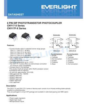
The CNY17-X and CNY17F-X series are families of 6-pin dual in-line package (DIP) optocouplers (also known as opto-isolators). Each device consists of a gallium arsenide infrared light-emitting diode (LED) optically coupled to a silicon NPN phototransistor. Its primary function is to provide electrical isolation between two circuits while allowing signal transmission via light. The main difference between the two series is: the CNY17-X series provides an external base connection pin (pin 6), while the CNY17F-X series does not have this connection (NC), resulting in lower noise sensitivity for the latter.
1.1 Core Advantages and Target Market
These devices are designed for applications requiring reliable signal isolation. Their core advantages include a high isolation voltage of up to 5000 Vrms, a compact DIP form factor suitable for through-hole mounting, and sorted current transfer ratio (CTR) groups for design consistency. They are certified by major international safety standards bodies (UL, cUL, VDE, SEMKO, etc.), making them well-suited for a wide range of industrial, consumer electronics, and power supply applications with stringent safety and noise immunity requirements.
2. In-depth Technical Parameter Analysis
2.1 Absolute Maximum Ratings
Absolute Maximum Ratings define the stress limits that may cause permanent damage to the device. These are not recommended operating conditions.
- Input Side (LED Terminal):Maximum Continuous Forward Current (IF) is 60 mA. A short-time (10 µs) peak forward current (IFM). The maximum reverse voltage (VR) across the LED is 6 V. At 25°C, the input power dissipation (PD) is 100 mW, derated by 3.8 mW/°C above 100°C.
- Output side (phototransistor side):Collector-emitter voltage (VCEO) and collector-base voltage (VCBO, CNY17-X only) are rated at 80 V. Emitter-collector (VECO) and emitter-base (VEBO) voltage is 7 V. At 25°C, the output power dissipation (PC) is 150 mW, derated at 9.0 mW/°C above 100°C.
- Total devices:Total device power dissipation (PTOT) must not exceed 200 mW.
- Isolation and Environment:Isolation voltage (VISO) is 5000 Vrms(AC, 1 minute). Operating temperature range (TOPR) is -55°C to +110°C. Maximum soldering temperature is 260°C for 10 seconds.
2.2 Electro-Optical Characteristics
These parameters define the performance of the device under typical operating conditions (unless otherwise specified, Ta= 25°C).
2.2.1 Halayen Shigarwa (Infrared LED)
- Forward Voltage (VF):At IF= 60 mA, the maximum value is 1.65 V. This is the voltage drop when the LED is conducting.
- Reverse Current (IR):At VRWhen = 6 V, the maximum value is 10 µA. This is the leakage current when the LED is reverse biased.
- Input capacitance (Cin):Typical value is 18 pF. This affects the high-frequency switching performance on the input side.
2.2.2 Halayen Fitarwa (Phototransistor)
- Dark current:When the LED is off (IF=0), there is leakage current. ICEO(collector-emitter) at VCETypical value is 50 nA at V=10V. ICBO(Collector-Base, only CNY17-X) at VCBMaximum value is 20 nA at V=10V.
- Breakdown voltage: BVCEOand BVCBOMinimum value is 80 V. BVECOMinimum value is 7 V.
- Output capacitor (CCE):Typical value is 8 pF. This affects the output switching speed.
2.3 Halayen Watsawa
These are the most critical parameters in signal coupling applications.
- Current Transfer Ratio (CTR):This is the output collector current (IC) to the input LED forward current (IFThe ratio, expressed as a percentage. Devices are divided into four distinct CTR ranges:
- CNY17-1 / CNY17F-1:CTR = 40% to 80% (at IF=10mA, VCE=5V conditions)
- CNY17-2 / CNY17F-2:CTR = 63% to 125%
- CNY17-3 / CNY17F-3:CTR = 100% to 200%
- CNY17-4 / CNY17F-4:CTR = 160% to 320%
- CTR at low current:At IFAt I = 1mA, a minimum CTR is specified (e.g., 13% for -1 grade, 56% for -4 grade), which is important for low-power or analog sensing applications.
- Saturation voltage (VCE(sat)):At IF=10mA, IC=2.5mA, maximum is 0.3 V. This is the voltage across the transistor when it is fully "on".
- Isolation resistance (RIO):Minimum value is 1011Ω. This indicates that the DC resistance between the input and output sides is extremely high.
- Input-output capacitance (CIO):Typical value is 0.5 pF. This small capacitance is key to achieving high common-mode transient immunity (CMTI).
2.4 Halayen Sauya
Dynamic performance is defined by turn-on/turn-off times and rise/fall times, which depend on test conditions.
- Condition 1 (VCC=10V, IC=2mA, RL=100Ω):
- Turn-on time (ton): Typical 10 µs, Maximum 12 µs.
- Turn-off time (toff): Typical value 9 µs, maximum value 12 µs.
- Rise time (tr): Typical value 6 µs, maximum value 10 µs.
- Fall time (tf): Typical value 8 µs, maximum value 10 µs.
- Condition 2 (VCC=5V, IF=10mA, RL=75Ω):
- Rise time (tr): Typical value 2 µs, maximum value 10 µs.
- Fall time (tf): Typical value 3 µs, maximum value 10 µs.
3. Grading System Description
Babban rarrabuwar waɗannan na'urorin haɗin haske ya dogara ne akanCurrent Transfer Ratio (CTR). Matakai huɗu (1, 2, 3, 4) suna ba da ƙananan da manyan ƙimar CTR waɗanda ke haɓaka sannu a hankali. Wannan yana ba masu zane damar zaɓar na'urar da ta dace da ribar siginar da ake buƙata, kuma ya tabbatar da daidaiton rukuni na samarwa. Misali, da'irar shigarwar dijital da ke buƙatar sigina mai ƙarfi da bayyananne na iya amfani da darajar -3 ko -4, yayin da da'irar da ke da hankali ga canje-canje na iya ƙayyadad da ƙaƙƙarfan darajar -1 mai ƙarancin riba.
4. Performance Curve Analysis
Takardar bayanai ta ambaci "Lankwila na Halayen Hasken Lantarki na Al'ada". Ko da yake ba a cikin rubutun da aka bayar cikakken bayani game da takamaiman jadawali, lankwila na al'ada na irin waɗannan na'urori sun haɗa da:
- CTR vs. Forward Current (IF):yana nuna yadda rabon watsawa ke canzawa tare da ƙarfin koriyar LED, yawanci yana kaiwa kololuwa a wani takamaiman ƙarfi.
- CTR vs. Temperature:Explain how CTR decreases with increasing ambient temperature, which is crucial for high-temperature operation.
- Collector Current (IC) vs. Collector-Emitter Voltage (VCE):Output characteristics of a phototransistor, showing the saturation region and the active region.
- Forward Voltage (VF) vs. Forward Current (IF):IV characteristics of an infrared LED.
These curves are essential for understanding device behavior under non-standard conditions and for optimizing circuit design.
5. Mechanical and Packaging Information
These devices are available in standard 6-pin DIP packages and offer multiple pin form options.
5.1 Package Dimensions and Options
- Standard DIP:The default through-hole package.
- Option M:Features "wide pin bending," providing a pin pitch of 0.4 inches (approximately 10.16 mm) for compatibility with wider PCB packages.
- Option S:Surface mount pin form. Designed specifically for reflow soldering process.
- Option S1:Surface mount pin form with a "low profile", suitable for applications with height restrictions.
Detailed dimension drawings (in millimeters) are provided for each option, specifying body dimensions, pin length, pin pitch, and mounting plane.
5.2 Pin Configuration and Polarity
Clear pin identification is crucial for proper installation.
- CNY17-X (with base pin):
- Anode (LED +)
- Cathode (LED -)
- No Connection
- Emitter (Phototransistor)
- Collector (Phototransistor)
- Base (Phototransistor, External Connection)
- CNY17F-X (Without Base Pin):
- Anode (LED +)
- Cathode (LED -)
- No Connection
- Emitter (Phototransistor)
- Collector (Phototransistor)
- No Connection
6. Soldering and Assembly Guide
The datasheet specifies a maximum soldering temperature of 260°C for 10 seconds. This typically applies to wave soldering or hand soldering for through-hole pins. For surface-mount options (S, S1), a standard infrared or convection reflow profile with a peak temperature not exceeding 260°C should be used. Precautions should be taken during handling to avoid excessive mechanical stress on the package. It should be stored in a dry, anti-static environment within the specified temperature range of -55°C to +125°C.
7. Packaging and Ordering Information
7.1 Model Numbering Rules
The part number follows the format:CNY17-XY(Z)-V或CNY17F-XY(Z)-V
- X:Part Number / CTR Grade (1, 2, 3, or 4).
- Y:Lead Form Option (S, S1, M, or leave blank for standard DIP).
- Z:Tape and Reel Packaging Option (TA, TB, or none). Applicable only for S and S1 options.
- V:Optional VDE certification mark.
7.2 Packaging Specifications
- Tube packaging:Standard DIP and option M are supplied in tubes, with 65 pieces per tube.
- Tape and reel packaging:Options S and S1 are available in tape and reel packaging. Options TA and TB contain 1000 pieces per reel.
8. Application Recommendations
8.1 Typical Application Circuit
The datasheet lists common uses: power supply regulators (for feedback isolation), digital logic inputs (for level shifting and noise isolation), and microprocessor inputs (for interfacing with noisy external signals). It shows a specific test circuit for switching times (Figure 11), which includes an input current-limiting resistor (RIN), an optional base-emitter resistor for CNY17-X (RBE), and a collector load resistor (RL).
8.2 Design Considerations
- LED Current Limiting:Always use a series resistor to limit the IFto the desired value, typically between 1 mA and 20 mA, to balance speed, CTR, and power consumption.
- Load Resistor (RL):The R on the collectorLvalue affects switching speed, output swing, and power consumption. A smaller RLshortens the fall time but reduces the output voltage swing.
- Noise Immunity (CNY17F-X):The CNY17F-X series has no external base connection, making it less susceptible to noise injection into the phototransistor base, thus preferred in electrically noisy environments.
- Speed and Current Trade-off:Higher IFtypically increases switching speed but also raises power consumption. Please refer to the switching time specifications under different test conditions.
- CTR Degradation:CTR decreases over the device's lifetime, especially under high operating temperatures and high currents. For long-term reliability, design with appropriate derating.
9. Technical Comparison
The key internal difference within the series is the presence or absence of an external base pin (present in CNY17-X, absent in CNY17F-X). CNY17-X offers greater design flexibility; the base pin can be left floating, connected to the emitter via a resistor (to improve speed by clearing stored charge), or used for specific bias configurations. CNY17F-X offers superior noise immunity because the phototransistor's base is entirely internal and inaccessible, which is a significant advantage in noisy industrial environments. Both series share the same isolation, voltage, and CTR specifications.
10. Frequently Asked Questions (Based on Technical Parameters)
Q: What are the main differences between the -1, -2, -3, and -4 grades?
A: The difference lies in the guaranteed range of the Current Transfer Ratio (CTR). Grade -4 has the highest gain (160-320%), while Grade -1 has the lowest gain (40-80%). Please select based on the required signal amplification factor in your circuit.
Q: When should I use CNY17F-X instead of CNY17-X?
A: Use CNY17F-X when operating in environments with significant electrical noise (e.g., motor drives, industrial control). The lack of an external base connection makes it inherently less susceptible to electromagnetic interference (EMI) coupling into the sensitive base region.
Q: How do I calculate the input series resistor for the LED?
A: Use Ohm's Law: RIN= (VCC_IN- VF) / IF. Assume VFTypical value ≈ 1.2V (max 1.65V). For example, using a 5V supply and expecting IFto be 10mA: RIN= (5V - 1.2V) / 0.01A = 380Ω. Use a standard 390Ω resistor.
Q: Can I use it for AC signal isolation?
A: Yes, but with limitations. The phototransistor output is unidirectional (DC). To transmit an AC signal, typically two optocouplers are needed (one for each half-cycle), or additional circuitry is required to bias the output into its linear region for analog transmission, although linearity is not a specified parameter for this device.
11. Practical Design Examples
Scene:Isolate the 3.3V microcontroller GPIO pin from the 24V industrial sensor signal.
- Device Selection:Select CNY17F-3 for good gain (100-200% CTR) and high noise immunity.
- Input Side (Microcontroller):The GPIO pin drives the LED through a current-limiting resistor. Assuming VGPIO_HIGH≈ 3.3V, target IF= 5mA: RIN= (3.3V - 1.2V) / 0.005A = 420Ω. Use 430Ω.
- Output side (sensor interface):Connect the phototransistor collector to the 24V power supply via a pull-up resistor (RL). The emitter is grounded. Select RLto ensure the output saturates when on and provides a valid logic high level when off. Assuming typical IC≈ CTR * IF= 150% * 5mA = 7.5mA, and the desired output logic high level when off is about 20V: RL≤ (24V - 20V) / (ICEO). Since ICEOThe maximum value is approximately 50nA, making almost any resistance value suitable for leakage current. For switching speed, a 10kΩ resistor is a common starting point. The output (collector node) now provides an isolated, inverted copy of the input signal.
12. Working Principle
An optocoupler works by converting an electrical signal into light, transmitting it across an electrically insulating barrier, and then converting the light back into an electrical signal. In the CNY17-X/F-X series, current (IF) flows through the infrared LED, causing it to emit photons. These photons pass through the transparent insulating molding compound and strike the base region of the silicon phototransistor. The photon energy generates electron-hole pairs in the base region, creating a base current that turns on the transistor, allowing collector current (IC) to flow. The ratio IC/IF即为CTR。输入和输出之间没有电气连接,提供了由模塑化合物的介电强度和内部引脚间距(爬电距离>7.6mm)决定的电气隔离。
13. Technology Trends
Optocoupler technology continues to evolve. While traditional phototransistor-based couplers like the CNY17 series remain popular for their cost-effectiveness and general-purpose isolation, trends are moving towards:
Higher Speeds:Haɓaka ƙwararrun masu haɗa haske da na'urori masu ƙara haɗin gwiwa (misali masu keɓance na dijital) don saurin canja wurin bayanai na Mbps da yawa.
Haɗin kai mafi girma:Haɗa tashoshi masu keɓance da yawa a cikin fakit ɗaya, ko haɗa keɓancewa da wasu ayyuka (kamar tuƙi na ƙofar ko hanyar haɗin ADC).
Ƙarfin aminci da tsawon rai mafi girma:Mai da hankali kan kayan aiki da ƙira, don rage raguwar CTR akan lokaci da zafin jiki.
Ƙananan girma:Ƙaura zuwa ƙananan fakiti masu haɗawa da saman (SOIC, SSOP), tare da kiyayewa ko haɓaka matakin keɓancewa. Zaɓuɓɓukan S da S1 na jerin CNY17 suna nuna wannan yanayin zuwa haɗaɗɗun saman.
Detailed Explanation of LED Specification Terminology
Complete Explanation of LED Technical Terminology
I. Core Indicators of Photoelectric Performance
| Terminology | Unit/Representation | Layman's Explanation | Why It Is Important |
|---|---|---|---|
| Luminous Efficacy | lm/W | The luminous flux emitted per watt of electrical power; higher values indicate greater energy efficiency. | Directly determines the energy efficiency rating of the luminaire and the electricity cost. |
| Luminous Flux | lm | Total light output from a light source, commonly known as "brightness". | Determines if a luminaire is bright enough. |
| Viewing Angle | ° (degrees), e.g., 120° | The angle at which light intensity drops to half, determining the width of the light beam. | Affects the illumination range and uniformity. |
| Yanayin zafi na launi (CCT) | K (Kelvin), misali 2700K/6500K | Launin haske mai dumi ko sanyi, ƙananan ƙima yana karkata zuwa rawaya/dumi, babban ƙima yana karkata zuwa fari/sanyi. | Yana ƙayyade yanayin haskakawa da wurin da ya dace. |
| Ma'aunin nuna launi (CRI / Ra) | Ba shi da raka'a, 0–100 | The ability of a light source to restore the true color of an object, Ra≥80 is recommended. | Affects color fidelity, used in high-demand places such as shopping malls and art galleries. |
| Color tolerance (SDCM) | MacAdam ellipse steps, e.g., "5-step" | A quantitative indicator of color consistency; the smaller the step number, the more consistent the color. | Ensures no color difference among the same batch of luminaires. |
| Dominant Wavelength | nm (nanometer), e.g., 620nm (red) | The wavelength value corresponding to the color of a colored LED. | Determines the hue of monochromatic LEDs such as red, yellow, and green. |
| Spectral Distribution | Wavelength vs. Intensity curve | Shows the intensity distribution of light emitted by the LED across various wavelengths. | Affects color rendering and color quality. |
II. Electrical Parameters
| Terminology | Symbol | Layman's Explanation | Design Considerations |
|---|---|---|---|
| Forward Voltage | Vf | The minimum voltage required to turn on an LED, similar to a "starting threshold". | The driving power supply voltage must be ≥ Vf; voltages add up when multiple LEDs are connected in series. |
| Forward Current | If | The current value that allows an LED to emit light normally. | Constant current drive is often used, as the current determines brightness and lifespan. |
| Maximum Pulse Current | Ifp | The peak current that can be withstood in a short time, used for dimming or flashing. | Pulse width and duty cycle must be strictly controlled, otherwise overheating damage will occur. |
| Reverse Voltage | Vr | The maximum reverse voltage that an LED can withstand; exceeding this may cause breakdown. | The circuit must be protected against reverse connection or voltage surges. |
| Thermal Resistance | Rth (°C/W) | The resistance to heat flow from the chip to the solder point; a lower value indicates better heat dissipation. | High thermal resistance requires a stronger heat dissipation design; otherwise, the junction temperature will increase. |
| Electrostatic Discharge Immunity (ESD Immunity) | V (HBM), e.g., 1000V | The ability to withstand electrostatic discharge; a higher value indicates greater resistance to damage from static electricity. | Anti-static measures must be implemented during production, especially for high-sensitivity LEDs. |
III. Thermal Management and Reliability
| Terminology | Maɗaukakin Ma'auni | Layman's Explanation | Tasiri |
|---|---|---|---|
| Junction Temperature | Tj(°C) | Ainihin zafin aiki a cikin guntu na LED. | Kowane raguwa na 10°C, rayuwa na iya tsawaita sau biyu; yawan zafi yana haifar da raguwar haske, karkatar launi. |
| Lumen Depreciation | L70 / L80 (hours) | The time required for brightness to drop to 70% or 80% of its initial value. | Directly defines the "useful life" of an LED. |
| Lumen Maintenance | % (e.g., 70%) | The percentage of remaining brightness after a period of use. | Characterizes the ability to maintain brightness after long-term use. |
| Color Shift | Δu′v′ or MacAdam Ellipse | The degree of color change during use. | Affects the color consistency of a lighting scene. |
| Thermal Aging | Decline in material performance. | Degradation of packaging materials due to prolonged high temperatures. | May lead to decreased brightness, color change, or open-circuit failure. |
IV. Packaging and Materials
| Terminology | Common Types | Layman's Explanation | Characteristics and Applications |
|---|---|---|---|
| Package Types | EMC, PPA, Ceramic | The housing material that protects the chip and provides optical and thermal interfaces. | EMC offers good heat resistance and low cost; ceramic provides superior heat dissipation and long lifespan. |
| Chip Structure | Front-side, Flip Chip | Chip electrode arrangement. | Flip Chip offers better heat dissipation and higher luminous efficacy, suitable for high power. |
| Phosphor coating | YAG, silicate, nitride | Coated on the blue LED chip, partially converts to yellow/red light, mixes to form white light. | Different phosphors affect luminous efficacy, color temperature, and color rendering. |
| Lens/Optical Design | Flat, microlens, total internal reflection | The optical structure on the package surface controls light distribution. | Determines the emission angle and light distribution curve. |
V. Quality Control and Binning
| Terminology | Grading Content | Layman's Explanation | Purpose |
|---|---|---|---|
| Luminous Flux Grading | Codes such as 2G, 2H | Grouped by brightness level, each group has a minimum/maximum lumen value. | Ensure consistent brightness within the same batch of products. |
| Voltage Binning | Codes such as 6W, 6X | Grouping based on forward voltage range. | Facilitates driver matching and improves system efficiency. |
| Color Binning | 5-step MacAdam ellipse | Group by color coordinates to ensure colors fall within an extremely narrow range. | Ensure color consistency to avoid color variation within the same luminaire. |
| Color temperature binning | 2700K, 3000K, etc. | Group by color temperature, each group has a corresponding coordinate range. | Meet the color temperature requirements of different scenarios. |
VI. Testing and Certification
| Terminology | Standard/Test | Layman's Explanation | Significance |
|---|---|---|---|
| LM-80 | Lumen Maintenance Test | Long-term operation under constant temperature conditions to record brightness attenuation data. | Used to estimate LED lifetime (combined with TM-21). |
| TM-21 | Lifetime extrapolation standard | Estimate lifetime under actual use conditions based on LM-80 data. | Provide scientific lifetime prediction. |
| IESNA standard | Illuminating Engineering Society Standard | Covers optical, electrical, and thermal test methods. | Industry-recognized testing basis. |
| RoHS / REACH | Environmental Certification | Ensures products are free from harmful substances (e.g., lead, mercury). | Market access requirements for entering international markets. |
| ENERGY STAR / DLC | Energy efficiency certification. | Energy efficiency and performance certification for lighting products. | Commonly used in government procurement and subsidy programs to enhance market competitiveness. |