Table of Contents
- 1. Product Overview
- 2. In-depth Technical Parameter Analysis
- 2.1 Electrical Characteristics
- 2.2 Maximum Ratings and Thermal Characteristics
- 3. Performance Curve Analysis
- 4. Mechanical and Packaging Information
- 4.1 Package Outline and Dimensions
- 4.2 Pin Configuration and Polarity Identification
- 5. Soldering and Assembly Guide
- 6. Application Recommendations
- 6.1 Typical Application Circuit
- 6.2 Design Considerations
- 7. Technical Comparison and Advantages
- 8. Frequently Asked Questions (Based on Technical Parameters)
- 8.1 What are the main advantages of the low Qc (6.4nC) specification?
- 8.2 The case is connected to the cathode. How does this affect my design?
- 8.3 Can I directly replace a silicon diode with the same voltage/current rating using this diode?
- 9. Uchambuzi wa kesi halisi ya muundo
- 10. Utangulizi mfupi wa kanuni ya uendeshaji
- 11. Technology Trends
1. Product Overview
This document details the specifications of a high-performance Silicon Carbide Schottky Barrier Diode. This device is specifically designed for power electronics applications that demand high efficiency, high-frequency operation, and superior thermal performance. Utilizing the standard TO-220-2L package, it provides a reliable solution for demanding power conversion circuits.
The core advantage of this diode lies in its Silicon Carbide technology. Compared to traditional silicon PN-junction diodes, this technology fundamentally offers a lower forward voltage drop and near-zero reverse recovery charge. This directly translates to lower conduction and switching losses, thereby enabling higher system efficiency and power density.
2. In-depth Technical Parameter Analysis
2.1 Electrical Characteristics
Key electrical parameters define the operating boundaries and performance of the device.
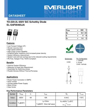
- Repetitive peak reverse voltage:650V. This is the maximum instantaneous reverse voltage that the diode can repeatedly withstand.
- Continuous Forward Current:4A. The maximum DC current that the device can conduct continuously, limited by its thermal characteristics.
- Forward Voltage:Under conditions of IF=4A, Tj=25°C, the typical value is 1.4V, and the maximum value is 1.75V. This low VF is a hallmark of silicon carbide Schottky technology, minimizing conduction losses.
- Reverse current:Under conditions of VR=520V, Tj=25°C, the typical value is 1µA. This low leakage current contributes to high efficiency in the off-state.
- Total capacitive charge:Under the condition of VR=400V, the typical value is 6.4nC. This is a key parameter for calculating switching losses, representing the charge that must be supplied/released in each switching cycle. Its low value supports high-speed switching.
2.2 Maximum Ratings and Thermal Characteristics
Absolute maximum ratings define the stress limits that may cause permanent damage.
- Surge non-repetitive forward current:Under Tc=25°C conditions, a 10ms half-sine wave pulse is 19A. This rating indicates the device's ability to handle short-circuit or surge current events.
- Junction temperature:Maximum 175°C. This is the upper limit for reliable operation.
- Total Power Dissipation:33W at Tc=25°C. This is the maximum power the package can dissipate under ideal thermal conditions at a specific case temperature.
- Junction-to-Case Thermal Resistance:The typical value is 4.5°C/W. This low thermal resistance is crucial for effectively transferring heat from the silicon die to the heat sink through the package case, enabling higher power handling capability.
3. Performance Curve Analysis
The datasheet provides several characteristic curves that are crucial for design and simulation.
- VF-IF characteristic curve:This graph shows the relationship between forward voltage and forward current at different junction temperatures. It is used to calculate conduction losses.
- VR-IR characteristic curve:It illustrates the relationship between reverse leakage current and reverse voltage and temperature, which is important for evaluating turn-off losses.
- VR-Ct characteristic curve:It shows how the junction capacitance of a diode varies with the applied reverse voltage. This nonlinear capacitance affects switching speed and ringing.
- Maximum forward current vs. case temperature characteristic curve:It depicts the derating of allowable forward current as the case temperature increases.
- Power dissipation derating curve:It shows how the maximum allowable power decreases as the case temperature increases.
- Surge Current vs. Pulse Width Characteristic Curve:It provides the surge current capability under different pulse widths, which is crucial for fuse selection and overload protection design.
- Stored Capacitor Energy vs. Reverse Voltage Characteristic Curve:A curve of stored capacitor energy versus reverse voltage was plotted, derived from the capacitance curve, for switching loss analysis.
- Transient Thermal Impedance Curve:It is crucial for evaluating thermal performance during short power pulses, when the thermal capacitance of the package becomes significant.
4. Mechanical and Packaging Information
4.1 Package Outline and Dimensions
The device employs the industry-standard TO-220-2L through-hole package. Key dimensions include:
- Overall length: 15.6 mm (typ.)
- Overall width: 9.99 mm (typ.)
- Total height: 4.5 mm (typical)
- Lead pitch: 5.08 mm (basic)
- Mounting hole distance: 8.70 mm (reference value)
- Mounting hole diameter: 1.70 mm (reference value)
This package is designed for easy mounting to a heat sink using M3 or 6-32 screws, with a specified maximum mounting torque of 8.8 N·m.
4.2 Pin Configuration and Polarity Identification
The pin arrangement is straightforward:
- Pin 1:Cathode
- Pin 2:Anode
- Case:It is electrically connected to the cathode. This connection is crucial for both circuit design and thermal management, as the case is typically used for heat dissipation.
The datasheet also provides a recommended pin surface mount pad layout for PCB design reference.
5. Soldering and Assembly Guide
Although this excerpt does not detail the specific reflow soldering profile, general considerations applicable to the TO-220 package are as follows:
- Operation:As with all semiconductor devices, observe standard ESD precautions.
- Installation:Apply thermal interface material between the package case and heat sink to minimize thermal resistance. Adhere to the specified maximum torque of 8.8 N·m to avoid damaging the package or PCB.
- Soldering:For through-hole mounting, standard wave soldering or manual soldering techniques can be used. The leads are suitable for bending. Follow the recommended pad layout for optimal solder joint formation and mechanical strength.
- Storage:Store in a dry, anti-static environment within the specified storage temperature range of -55°C to +175°C.
6. Application Recommendations
6.1 Typical Application Circuit
The datasheet clearly lists several key application areas where the advantages of silicon carbide Schottky diodes are most prominent.
- Power Factor Correction in Switching Power Supplies.High switching speed and low Qc significantly reduce the switching loss of the PFC stage boost diode, improving overall efficiency, especially at high line frequencies.
- Solar Inverter:Used for output rectification or freewheeling path to minimize losses, thereby improving the energy harvesting efficiency of photovoltaic panels.
- Uninterruptible Power Supply:Improve the efficiency of the inverter/charger section, thereby reducing operating costs and cooling requirements.
- Motor Drive:Used as freewheeling diodes in the inverter bridge to achieve higher switching frequencies, resulting in quieter motor operation and more precise control.
- Data Center Power Supply:The pursuit of high efficiency in server power supplies makes the low-loss characteristics of this diode highly valuable.
6.2 Design Considerations
- Thermal Management:Low junction-to-case thermal resistance helps with effective heat dissipation, but under worst-case conditions, a properly sized heatsink is still required to keep the junction temperature below 175°C. Please use the power derating curve during design.
- Switching Behavior:Although the recovery loss is negligible, the capacitive switching behavior still needs to be considered. Low Qc can minimize the turn-on loss of the relative switch in the bridge configuration.
- Parallel operation:The positive temperature coefficient of the forward voltage helps current sharing when multiple diodes are connected in parallel, preventing thermal runaway.
- Snubber circuit:Due to the extremely fast switching speed, attention should be paid to parasitic inductance in the circuit layout to minimize voltage overshoot and ringing. Depending on the layout, an RC snubber circuit may be required.
7. Technical Comparison and Advantages
Compared to standard silicon fast recovery diodes or even ultrafast recovery diodes, this silicon carbide Schottky diode offers significant advantages:
- Nearly zero reverse recovery charge:Unlike PN junction diodes, Schottky diodes are majority carrier devices. They have no stored minority carrier charge, so no recovery is needed when switching from forward bias to reverse bias. This eliminates reverse recovery loss and associated noise.
- Lower forward voltage drop:At typical operating currents, the VF of this SiC diode is comparable to or lower than that of high-voltage silicon Schottky diodes.
- High-temperature operation capability:The material properties of silicon carbide allow for reliable operation at higher junction temperatures.
- High-Frequency Capability:The combination of low Qc and no Qrr enables operation at higher switching frequencies, thereby allowing the use of smaller magnetic components and capacitors in the system.
8. Frequently Asked Questions (Based on Technical Parameters)
8.1 What are the main advantages of low Qc specification?
Low total capacitive charge directly translates to lower switching losses. In each switching cycle, the energy required to charge and discharge the diode junction capacitance is lost. A lower Qc means less energy wasted per cycle, enabling operation at higher frequencies with higher efficiency.
8.2 The case is connected to the cathode. How does this affect my design?
This connection is crucial for two reasons:Electrical aspect:The heatsink will be at cathode potential. If the cathode in the circuit is not at ground potential, it is necessary to ensure proper insulation between the heatsink and other components or the chassis ground. Typically, insulating washers and sleeves are required.Thermal aspects:It provides an excellent low-impedance thermal path from the silicon chip to the external heat sink through the metal case, which is crucial for heat dissipation.
8.3 Can I directly replace a silicon diode with the same voltage/current rating using this diode?
Usually possible, but direct replacement may not yield optimal results. Due to lower losses, silicon carbide diodes may operate at lower temperatures. However, you must re-evaluate: 1)Snubber/Ringing:Faster switching speeds may more easily excite parasitic inductance, potentially requiring layout adjustments or the addition of snubber circuits. 2)Gate Drive:If replacing the freewheeling diode in the bridge circuit, the opposing switch may experience a higher turn-on current spike due to the diode's capacitance. The driver's capability should be checked.3)Thermal design:Although the losses are lower, it is still necessary to verify the new loss calculations and ensure that the heat sink remains adequate, even though it may now be oversized.
9. Uchambuzi wa kesi halisi ya muundo
Scenario:Design a 500W, 100kHz boost-type power factor correction stage with 400VDC output.
Reason for Selection:The boost diode in a PFC circuit operates in continuous conduction mode at high frequencies. A standard 600V silicon ultrafast recovery diode may have a Qrr of 50-100nC and a Vf of 1.7-2.0V. Its switching and conduction losses will be very significant.
Using this silicon carbide Schottky diode:
- Switching Loss:Reverse recovery loss is eliminated. The remaining capacitive switching loss is based on Qc=6.4nC, which is an order of magnitude lower than the Qrr of silicon diodes.
- Conduction Loss:Typical Vf is 1.4V compared to 1.8V, reducing conduction loss by over 20%.
- Result:Total diode losses are significantly reduced. This enables: a) improved system efficiency to meet stricter standards; or b) operation at higher switching frequencies, allowing the use of smaller, lighter boost inductors. The reduced heat generation also simplifies thermal management, potentially permitting the use of smaller heat sinks.
10. Utangulizi mfupi wa kanuni ya uendeshaji
The Schottky barrier diode is formed by a metal-semiconductor junction, which is different from the P-N semiconductor junction of a standard diode. In this silicon carbide Schottky diode, the metal contact forms a connection with the silicon carbide.
The fundamental difference lies in charge transport. In a PN diode, forward conduction involves the injection and storage of minority carriers. When the voltage is reversed, these stored carriers must be removed before the diode can block the voltage, resulting in reverse recovery current and losses.
In a Schottky diode, conduction is achieved by the flow of majority carriers across the metal-semiconductor barrier. There is no minority carrier injection and storage. Consequently, when the applied voltage reverses, the diode can cease conduction almost instantaneously. This leads to its characteristic near-zero reverse recovery time and charge. The silicon carbide substrate provides the material properties necessary to achieve high breakdown voltage while maintaining a relatively low forward voltage drop and excellent thermal conductivity.
11. Technology Trends
Silicon carbide power devices represent a significant trend in the field of power electronics, driven by the global demand for higher efficiency, power density, and reliability. The main trends include:
- Voltage Rating Expansion:While 650V is the mainstream voltage for applications such as PFC and solar, silicon carbide Schottky diodes are now commonly available in 1200V and 1700V ratings, directly competing with silicon IGBT freewheeling diodes and enabling new applications such as EV traction inverters and industrial drives.
- Integration:The trend is to co-package silicon carbide Schottky diodes with silicon or silicon carbide MOSFETs in common power modules, creating optimized "half-bridge" or "full-bridge" building blocks to minimize parasitic inductance.
- Cost Reduction:As wafer manufacturing scales up and defect density decreases, the cost premium of silicon carbide relative to silicon continues to narrow, accelerating its adoption in cost-sensitive, high-volume applications.
- Complementary Technologies:The development of silicon carbide MOSFETs and JFETs is synergistic. Using silicon carbide Schottky diodes as freewheeling or boost diodes alongside silicon carbide switches enables the creation of all-silicon-carbide power stages capable of operating at very high frequencies and temperatures with minimal losses.
The devices described in this datasheet are fundamental components in the broader technological shift toward wide-bandgap semiconductors within the field of power conversion.
Detailed Explanation of LED Specification Terminology
Complete Explanation of LED Technical Terminology
I. Core Indicators of Optoelectronic Performance
| Terminology | Units/Representation | Popular Explanation | Why It Is Important |
|---|---|---|---|
| Luminous Efficacy | lm/W (lumens per watt) | The luminous flux emitted per watt of electrical power, higher values indicate greater energy efficiency. | Directly determines the energy efficiency rating and electricity cost of the lighting fixture. |
| Luminous Flux | lm (lumen) | The total amount of light emitted by a light source, commonly known as "brightness". | Determines whether a light fixture is bright enough. |
| Viewing Angle | ° (degrees), e.g., 120° | The angle at which the light intensity drops to half determines the beam width. | Affects the illumination range and uniformity. |
| Correlated Color Temperature (CCT) | K (Kelvin), e.g., 2700K/6500K | The warmth or coolness of light color; lower values are yellowish/warm, higher values are whitish/cool. | Determining the lighting atmosphere and applicable scenarios. |
| Color Rendering Index (CRI / Ra) | Unitless, 0–100 | The ability of a light source to restore the true color of an object, Ra≥80 is recommended. | Affects color authenticity, used in high-demand places such as shopping malls and art galleries. |
| SDCM (Standard Deviation of Color Matching) | MacAdam ellipse steps, e.g., "5-step" | A quantitative indicator of color consistency; a smaller step number indicates higher color consistency. | Ensure no color difference among the same batch of luminaires. |
| Dominant Wavelength | nm (nanometer), misali 620nm (ja) | Rangi ya LED ya rangi inayolingana na thamani ya urefu wa wimbi. | Kuamua rangi ya LED ya rangi moja kama nyekundu, manjano, kijani, n.k. |
| Spectral Distribution | Wavelength vs. Intensity Curve | Display the intensity distribution of light emitted by the LED across various wavelengths. | Affects color rendering and color quality. |
II. Electrical Parameters
| Terminology | Symbol | Popular Explanation | Design Considerations |
|---|---|---|---|
| Forward Voltage | Vf | The minimum voltage required to light up an LED, similar to a "starting threshold". | The driving power supply voltage must be ≥Vf, and the voltage adds up when multiple LEDs are connected in series. |
| Forward Current | If | The current value that makes the LED emit light normally. | Constant current drive is often used, as the current determines brightness and lifespan. |
| Maximum Pulse Current (Pulse Current) | Ifp | Peak current that can be withstood in a short time, used for dimming or flashing. | Pulse width and duty cycle must be strictly controlled, otherwise overheating damage. |
| Reverse Voltage | Vr | The maximum reverse voltage that an LED can withstand; exceeding it may cause breakdown. | Circuit ina buƙatar hana karkatar da baya ko kuma ƙarfin wutar lantarki. |
| Thermal Resistance | Rth (°C/W) | The resistance to heat flow from the chip to the solder joint. A lower value indicates better heat dissipation. | High thermal resistance requires a more robust thermal design; otherwise, the junction temperature will increase. |
| ESD Immunity | V (HBM), e.g., 1000V | The higher the ESD immunity rating, the more resistant the device is to electrostatic damage. | Anti-static measures must be taken during production, especially for high-sensitivity LEDs. |
III. Thermal Management and Reliability
| Terminology | Key Metrics | Popular Explanation | Impact |
|---|---|---|---|
| Junction Temperature | Tj (°C) | The actual operating temperature inside the LED chip. | For every 10°C reduction, lifespan may double; excessively high temperatures cause lumen depreciation and color shift. |
| Lumen Depreciation | L70 / L80 (hours) | The time required for brightness to drop to 70% or 80% of its initial value. | Directly defines the "lifetime" of an LED. |
| Lumen Maintenance | % (e.g., 70%) | The percentage of remaining brightness after a period of use. | Characterizes the ability to maintain brightness after long-term use. |
| Color Shift | Δu′v′ or MacAdam ellipse | The degree of color change during use. | Affects the color consistency of the lighting scene. |
| Thermal Aging | Material performance degradation | Deterioration of packaging materials due to prolonged high temperatures. | May lead to decreased brightness, color shift, or open-circuit failure. |
IV. Packaging and Materials
| Terminology | Common Types | Popular Explanation | Characteristics and Applications |
|---|---|---|---|
| Packaging Type | EMC, PPA, Ceramic | The housing material that protects the chip and provides optical and thermal interfaces. | EMC tahan panas baik, biaya rendah; keramik pendinginan unggul, umur panjang. |
| Struktur chip | Face-up, Flip Chip | Chip electrode arrangement method. | Flip Chip offers better heat dissipation and higher luminous efficacy, suitable for high-power applications. |
| Phosphor coating | YAG, silicate, nitride | Covered on the blue light chip, partially converted into yellow/red light, mixed into white light. | Different phosphors affect luminous efficacy, color temperature, and color rendering. |
| Lens/Optical design | Plane, Microlens, Total Internal Reflection | Optical structure on the encapsulation surface, controlling light distribution. | Determine the beam angle and light distribution curve. |
V. Quality Control and Binning
| Terminology | Binning Content | Popular Explanation | Purpose |
|---|---|---|---|
| Luminous Flux Classification | Codes such as 2G, 2H | Group by brightness level, each group has a minimum/maximum lumen value. | Ensure consistent brightness within the same batch of products. |
| Voltage binning | Codes such as 6W, 6X | Group by forward voltage range. | Facilitates driver matching and improves system efficiency. |
| Color binning | 5-step MacAdam Ellipse | Group by color coordinates to ensure colors fall within a minimal range. | Ensure color consistency to avoid uneven color within the same luminaire. |
| Color temperature binning | 2700K, 3000K, etc. | Grouped by color temperature, each group has a corresponding coordinate range. | Meet the color temperature requirements of different scenarios. |
VI. Testing and Certification
| Terminology | Standard/Test | Popular Explanation | Significance |
|---|---|---|---|
| LM-80 | Lumen Maintenance Test | Record brightness attenuation data under constant temperature conditions over long-term operation. | Used for estimating LED lifetime (in conjunction with TM-21). |
| TM-21 | Standard for Life Projection | Projecting lifetime under actual use conditions based on LM-80 data. | Provide scientific life prediction. |
| IESNA Standard | Illuminating Engineering Society Standard | Covers optical, electrical, and thermal testing methods. | Industry-recognized testing basis. |
| RoHS / REACH | Environmental Certification | Ensure products are free from hazardous substances (e.g., lead, mercury). | Market access requirements for entering the international market. |
| ENERGY STAR / DLC | Energy Efficiency Certification | Energy Efficiency and Performance Certification for Lighting Products. | Commonly used in government procurement, subsidy programs to enhance market competitiveness. |