1. Product Overview
This document details the specifications for a high-performance Silicon Carbide (SiC) Schottky Barrier Diode (SBD) housed in a TO-220-2L package. The device is engineered for high-voltage, high-frequency power conversion applications where efficiency, thermal management, and switching speed are critical. SiC technology offers significant advantages over traditional silicon diodes, primarily due to its superior material properties.
The core advantage of this diode lies in its Schottky barrier construction using Silicon Carbide. Unlike conventional PN-junction diodes, Schottky diodes are majority carrier devices, which fundamentally eliminates reverse recovery charge (Qrr) and the associated switching losses. This specific SiC implementation allows for a high blocking voltage of 650V while maintaining a relatively low forward voltage drop (VF) and minimal capacitive charge (Qc), enabling operation at much higher frequencies than silicon alternatives.
1.1 Key Features and Benefits
Siffofi na farko na wannan diode suna fassara kai tsaye zuwa fa'idodin matakin tsarin ga masu zane:
- Ƙarancin Ƙarfin Gaba (VF = 1.5V na yau da kullun a 6A): Reduces conduction losses, directly improving system efficiency and generating less heat during operation.
- High-Speed Switching with No Reverse Recovery: As a Schottky device, it has essentially no reverse recovery time or charge (Qrr). This minimizes switching losses, allows for higher frequency operation, and reduces electromagnetic interference (EMI).
- High Surge Current Capability (IFSM = 24A): Provides robustness against current transients and inrush conditions commonly encountered in power supplies and motor drives.
- High Junction Temperature (TJ,max = 175°C): Enables operation in high ambient temperature environments or allows for the use of smaller heat sinks, contributing to system size and cost reduction.
- Parallel Operation: The positive temperature coefficient of the forward voltage characteristic helps prevent thermal runaway, making it safer to parallel multiple devices for higher current applications.
- Environmental Compliance: The device is Pb-Free, Halogen Free, and RoHS Compliant, meeting modern environmental regulations.
1.2 Target Applications
This diode is ideally suited for a wide range of power electronics applications, including but not limited to:
- Power Factor Correction (PFC) circuits in Switched-Mode Power Supplies (SMPS): Its fast switching and high voltage rating make it perfect for boost PFC stages, improving overall power supply efficiency and power quality.
- Solar Inverters: Used in the boost converter or freewheeling diode positions to maximize energy harvest and conversion efficiency from photovoltaic panels.
- Uninterruptible Power Supplies (UPS): Enhances the efficiency and power density of the rectifier and inverter stages.
- Motor Drives: Serves as a freewheeling or clamping diode in inverter bridges, enabling faster switching and reducing losses in variable frequency drives (VFDs).
- Data Center Power Distribution: Contributes to higher efficiency in server power supplies and power distribution units, reducing operational costs and cooling requirements.
2. In-Depth Technical Parameter Analysis
This section provides a detailed, objective interpretation of the key electrical and thermal parameters specified in the datasheet.
2.1 Maximum Ratings and Absolute Limits
These are stress limits that must not be exceeded under any operating condition to ensure reliability and prevent permanent damage.
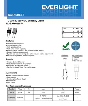
- Repetitive Peak Reverse Voltage (VRRM): 650V - This is the maximum instantaneous reverse voltage the diode can withstand repeatedly. Designing with a sufficient derating margin (e.g., 20-30% below this value for the maximum expected system voltage) is crucial for long-term reliability.
- Continuous Forward Current (IF): 6A - This is the maximum DC current the device can carry continuously when the case temperature (TC) is at 25\u00b0C. In real applications, the case temperature will be higher, so the usable continuous current is derated based on the thermal resistance and ambient conditions (see Thermal Characteristics).
- Surge Non-Repetitive Forward Current (IFSM): 24A - This rating indicates the diode's ability to handle a single, short-duration (10ms half-sine wave) surge current, such as during startup or fault conditions. This is a key parameter for robustness.
- Junction Temperature (TJ): 175\u00b0C - The maximum allowable temperature of the semiconductor die itself. Operation above this limit can cause immediate failure or accelerated degradation.
2.2 Electrical Characteristics
These are the typical performance parameters under specified test conditions.
- Forward Voltage (VF): 1.5V (Typ) at IF=6A, TJ=25\u00b0C - This is a critical parameter for conduction loss calculation (Ploss = VF * IF). Note that VF increases with junction temperature (to 1.9V max at 175°C), which is a positive temperature coefficient. This characteristic aids in current sharing when devices are paralleled.
- Reverse Leakage Current (IR): 0.8µA (Typ) at VR=520V, TJ=25°C - This is the small current that flows when the diode is reverse-biased. It increases significantly with temperature (9µA typ at 175°C), contributing to off-state losses, especially at high temperatures.
- Total Capacitive Charge (QC): 10nC (Typ) at VR=400V - This parameter quantifies the charge associated with the diode's junction capacitance. During switching, this charge must be supplied or removed, contributing to switching losses. The low QC value is a key advantage of SiC Schottky diodes, enabling high-frequency operation.
- Capacitance Stored Energy (EC): 1.5µJ (Typ) at VR=400V - Represents the energy stored in the diode's capacitance at a given reverse voltage (EC = 0.5 * C * V^2). This energy is dissipated during each switching cycle, contributing to losses.
2.3 Thermal Characteristics
Thermal management is paramount for reliable operation and achieving the rated current.
- Thermal Resistance, Junction-to-Case (RθJC): 2.1°C/W (Typ) - This is the resistance to heat flow from the semiconductor junction to the exterior case of the TO-220 package. A lower value indicates better heat transfer from the die. This parameter is used to calculate the junction temperature rise above the case temperature: ΔTJ = PD * RθJC, where PD is the power dissipation.
- Total Power Dissipation (PD): 71W at TC=25°C - This is the maximum power the device can dissipate when the case is held at 25°C. In practice, this is a theoretical limit used for calculating derating. The actual maximum power dissipation is determined by the maximum junction temperature (175°C), the thermal resistance, and the heatsink/ambient temperature.
3. Performance Curve Analysis
The typical performance graphs provide visual insight into the device's behavior under various operating conditions.
3.1 VF-IF Characteristics
This graph shows the relationship between forward voltage and forward current at different junction temperatures. Key observations: The curve is exponential at very low currents and becomes more linear at higher currents. The positive temperature coefficient is evident, as the curve shifts upward for higher temperatures. This graph is essential for calculating precise conduction losses at specific operating points.
3.2 VR-IR Characteristics
This plot illustrates the reverse leakage current as a function of reverse voltage, typically at multiple temperatures. It demonstrates how leakage current remains relatively low until approaching the breakdown region and how it increases exponentially with temperature. This information is vital for estimating off-state losses in high-temperature applications.
3.3 VR-Ct Characteristics
This curve displays the total diode capacitance (Ct) versus reverse voltage (VR). The capacitance decreases non-linearly as the reverse voltage increases (due to the widening of the depletion region). This variable capacitance affects the switching dynamics and the QC parameter.
3.4 Maximum Ip – TC Characteristics
This derating curve shows how the maximum allowable continuous forward current (IF) decreases as the case temperature (TC) increases. It is a direct application of the thermal limits: to keep the junction below 175°C, less current can be passed as the case gets hotter. This is the primary guide for heatsink selection.
3.5 Transient Thermal Impedance
This graph plots transient thermal resistance (ZθJC) against pulse width. It is crucial for evaluating temperature rise during short current pulses or repetitive switching events. The thermal mass of the package causes the effective resistance to be lower for very short pulses than the steady-state RθJC.
4. Mechanical and Package Information
4.1 Package Outline and Dimensions
The device uses the industry-standard TO-220-2L package. The detailed dimensional drawing provides minimum, typical, and maximum values for all critical features, including overall height (A: 4.5mm typ), lead length (L: 13.18mm typ), and mounting hole spacing (D1: 9.05mm typ). Adherence to these dimensions is necessary for proper PCB layout and mechanical mounting.
4.2 Pin Configuration and Polarity
The TO-220-2L package has two leads:
1. Pin 1: Cathode (K).
2. Pin 2: Anode (A).
Bugu da kari, guntun karfe (akwati) na kunshin yana haɗe da Cathode ta hanyar lantarki. Wannan muhimmin la'akari ne na aminci da ƙira. Dole ne a keɓe guntun daga sauran kewaye (misali, ta amfani da wanka mai rufewa da hannun riga) sai dai idan gama kewaye shima yana da ƙarfin Cathode.
4.3 Recommended PCB Pad Layout
An ba da shawarar sawun ƙafa don hawa saman ginshiƙan da aka ƙirƙira. Wannan shimfiɗa yana tabbatar da ingantaccen haɗin gwiwar solder, ƙarfin injiniya, da taimakon zafi yayin ayyukan wave ko reflow soldering.
5. Mounting and Handling Guidelines
5.1 Mounting Torque
The specified mounting torque for the screw used to attach the package to a heatsink is 8.8 N·m (or equivalent in lbf-in) for an M3 or 6-32 screw. Applying the correct torque is essential: insufficient torque leads to high thermal resistance, while excessive torque can damage the package or the PCB.
5.2 Thermal Interface
To minimize the thermal resistance between the device case and the heatsink, a thin layer of thermal interface material (TIM), such as grease, gap pad, or phase-change material, must be used. The TIM fills microscopic air gaps, significantly improving heat transfer.
5.3 Yanayin Ajiya
Ya kamata a adana na'urar a cikin ƙayyadaddun kewayon zafin ajiya na -55°C zuwa +175°C a cikin busasshiyar muhalli mara lalata. Bayanan Ma'aunin Danshi (MSL), idan ya dace ga jagororin, ya kamata a tuntubi daga masana'anta don kulawa daidai kafin a yi amfani da su.
6. Application Design Considerations
6.1 Snubber Circuits
While SiC Schottky diodes have negligible reverse recovery, their junction capacitance can still interact with circuit parasitics (stray inductance) to cause voltage overshoot and ringing during turn-off. A simple RC snubber network across the diode may be necessary to dampen these oscillations and reduce EMI, especially in high-di/dt circuits.
6.2 Abubuwan da ake la'akari da tuƙi na Gate don Maɓallan Abokin Tafiya
Lokacin da aka yi amfani da wannan diode azaman diode mai kyauta ko diode mai haɓakawa tare da MOSFET ko IGBT, saurin sauyawar sa na iya lalacewa ta hanyar jinkirin kunna babban maɓalli. Tabbatar da tsari mai ƙarancin inductance da ƙaƙƙarfan, mai sauri direban ƙofa don maɓallin aiki yana da mahimmanci don amfani da gudun diode gabaɗaya da rage yawan gudanar da diode na jikin MOSFET.
6.3 Parallel Operation
VF's positive temperature coefficient facilitates current sharing in parallel configurations. However, for optimal dynamic and static current balance, a symmetrical layout is mandatory. This includes identical trace lengths and impedances to each diode's anode and cathode, and mounting them on a common heatsink to equalize temperatures.
7. Technical Comparison and Advantages
Compared to standard silicon fast recovery diodes (FRDs) or even silicon carbide MOSFET body diodes, this SiC Schottky diode offers distinct advantages:
- vs. Silicon FRDs: The most significant difference is the absence of reverse recovery charge (Qrr). A silicon FRD has substantial Qrr, causing large current spikes during commutation, leading to high switching losses, increased stress on the main switch, and greater EMI. The SiC Schottky eliminates this, enabling higher efficiency and frequency.
- vs. Silicon PN Diodes: Beyond recovery, the SiC device typically has a lower forward voltage at high temperatures and a much higher maximum junction temperature (175\u00b0C vs. 150\u00b0C for many silicon parts), allowing for more compact thermal design.
- vs. Lower Voltage Silicon Schottky Diodes: Traditional silicon Schottky diodes are limited to blocking voltages below about 200V due to high leakage current. SiC material properties allow the Schottky barrier design to be extended to 650V and beyond while maintaining excellent switching and conduction performance.
8. Frequently Asked Questions (FAQs)
8.1 Does this diode require a reverse recovery snubber?
No, it does not require a snubber to manage reverse recovery losses, as it has essentially no Qrr. However, an RC snubber might still be beneficial to damp voltage ringing caused by the interaction of its junction capacitance with circuit stray inductance.
8.2 How do I calculate the power dissipation?
Power dissipation has two main components: conduction loss and capacitive switching loss.
Conduction Loss: P_cond = VF * IF * Duty_Cycle (where VF is taken at the operating current and junction temperature).
Capacitive Switching Loss: P_sw_cap = 0.5 * C * V^2 * f_sw (or use the EC value provided). Since Qrr loss is zero, it is not included. The total PD is the sum of these, which is used with the thermal resistance to calculate junction temperature rise.
8.3 Can I use it in a 400V DC bus application?
Yes, a 650V VRRM diode is appropriately rated for a 400V DC bus. Common design practice is to derate by 20-30%, meaning the maximum repetitive reverse voltage should be 1.2-1.3 times the maximum system voltage. 650V / 1.3 = 500V, which provides a good safety margin for a 400V bus, accounting for transients and spikes.
8.4 Is the metal tab live?
Yes. The datasheet clearly states "CASE: Cathode." The metal tab is electrically connected to the cathode pin. It must be insulated from the heatsink (which is often connected to earth or chassis ground) unless the cathode is at the same potential.
9. Misalin Ƙira na Aiki
Yanayi: Designing a 1.5kW boost Power Factor Correction (PFC) stage with an output of 400V DC from a universal AC input (85-265VAC). The switching frequency is set to 100 kHz for magnetics size reduction.
Diode Selection Rationale: The boost diode must block the output voltage (400V plus ripple). Voltage spikes are expected. The 650V rating provides sufficient margin. At 100 kHz, switching losses are dominant. A standard silicon FRD would have prohibitively high Qrr losses at this frequency. This SiC Schottky diode, with its near-zero Qrr and low QC, minimizes switching losses, making high-frequency operation feasible and efficient. The estimated average current in the diode is calculated from the output power and voltage. The 6A continuous rating, when properly heatsinked, is suitable for this power level. The low VF also keeps conduction losses manageable.
Thermal Design: Using the estimated total power dissipation (P_cond + P_sw_cap), the RθJC, and the target maximum junction temperature (e.g., 125°C for a reliability margin), the required heatsink thermal resistance (RθSA) can be calculated to ensure the device operates within safe limits.
10. Technology Background and Trends
10.1 Silicon Carbide (SiC) Material Advantages
Silicon Carbide is a wide bandgap semiconductor material. Its key properties include a higher critical electric field (allowing for thinner, higher-voltage drift layers), higher thermal conductivity (better heat dissipation), and the ability to operate at much higher temperatures than silicon. These intrinsic properties are what enable the high-voltage, high-temperature, and high-frequency performance of SiC Schottky diodes and other SiC power devices.
10.2 Market and Technology Trends
The adoption of SiC power devices is accelerating, driven by global demands for higher energy efficiency, power density, and the electrification of transportation and industry. SiC diodes and MOSFETs are becoming standard in high-performance solar inverters, electric vehicle onboard chargers and traction drives, and advanced server power supplies. The trend is towards higher voltage ratings (e.g., 1200V, 1700V) for industrial and automotive applications, lower specific on-resistance for MOSFETs, and the integration of SiC devices into power modules. As manufacturing volumes increase and costs decrease, SiC technology is moving from premium applications into broader mainstream markets.
LED Specification Terminology
Complete explanation of LED technical terms
Photoelectric Performance
| Term | Unit/Representation | Simple Explanation | Why Important |
|---|---|---|---|
| Luminous Efficacy | lm/W (lumens per watt) | Light output per watt of electricity, higher means more energy efficient. | Directly determines energy efficiency grade and electricity cost. |
| Luminous Flux | lm (lumens) | Total light emitted by source, commonly called "brightness". | Determines if the light is bright enough. |
| Viewing Angle | ° (degrees), e.g., 120° | Kwanin da ƙarfin haske ya ragu zuwa rabi, yana ƙayyade faɗin katako. | Yana shafar kewayon haskakawa da daidaito. |
| CCT (Color Temperature) | K (Kelvin), e.g., 2700K/6500K | Warmth/coolness of light, lower values yellowish/warm, higher whitish/cool. | Yana ƙayyade yanayin haske da yanayin da ya dace. |
| CRI / Ra | Unitless, 0–100 | Ability to render object colors accurately, Ra≥80 is good. | Affects color authenticity, used in high-demand places like malls, museums. |
| SDCM | MacAdam ellipse steps, e.g., "5-step" | Metric ya Consistency ya Rangi, hatua ndogo zina maana rangi inayolingana zaidi. | Inahakikisha rangi sawa kwenye kundi moja la LEDs. |
| Dominant Wavelength | nm (nanometers), e.g., 620nm (red) | Wavelength corresponding to color of colored LEDs. | Determines hue of red, yellow, green monochrome LEDs. |
| Spectral Distribution | Wavelength vs intensity curve | Shows intensity distribution across wavelengths. | Affects color rendering and quality. |
Electrical Parameters
| Term | Symbol | Simple Explanation | Design Considerations |
|---|---|---|---|
| Forward Voltage | Vf | Minimum voltage to turn on LED, like "starting threshold". | Driver voltage must be ≥Vf, voltages add up for series LEDs. |
| Forward Current | If | Current value for normal LED operation. | Usually constant current drive, current determines brightness & lifespan. |
| Max Pulse Current | Ifp | Peak current tolerable for short periods, used for dimming or flashing. | Pulse width & duty cycle must be strictly controlled to avoid damage. |
| Reverse Voltage | Vr | Max reverse voltage LED can withstand, beyond may cause breakdown. | Circuit must prevent reverse connection or voltage spikes. |
| Thermal Resistance | Rth (°C/W) | Resistance to heat transfer from chip to solder, lower is better. | High thermal resistance requires stronger heat dissipation. |
| ESD Immunity | V (HBM), e.g., 1000V | Ability to withstand electrostatic discharge, higher means less vulnerable. | Anti-static measures needed in production, especially for sensitive LEDs. |
Thermal Management & Reliability
| Term | Key Metric | Simple Explanation | Impact |
|---|---|---|---|
| Junction Temperature | Tj (°C) | Actual operating temperature inside LED chip. | Every 10°C reduction may double lifespan; too high causes light decay, color shift. |
| Lumen Depreciation | L70 / L80 (hours) | Time for brightness to drop to 70% or 80% of initial. | Directly defines LED "service life". |
| Lumen Maintenance | % (e.g., 70%) | Percentage of brightness retained after time. | Indicates brightness retention over long-term use. |
| Color Shift | Δu′v′ or MacAdam ellipse | Degree of color change during use. | Affects color consistency in lighting scenes. |
| Thermal Aging | Material degradation | Deterioration due to long-term high temperature. | May cause brightness drop, color change, or open-circuit failure. |
Packaging & Materials
| Term | Common Types | Simple Explanation | Features & Applications |
|---|---|---|---|
| Package Type | EMC, PPA, Ceramic | Housing material protecting chip, providing optical/thermal interface. | EMC: good heat resistance, low cost; Ceramic: better heat dissipation, longer life. |
| Chip Structure | Front, Flip Chip | Chip electrode arrangement. | Flip chip: kona mafuta bora, ufanisi mkubwa, kwa nguvu kubwa. |
| Phosphor Coating | YAG, Silicate, Nitride | Covers blue chip, converts some to yellow/red, mixes to white. | Different phosphors affect efficacy, CCT, and CRI. |
| Lens/Optics | Flat, Microlens, TIR | Optical structure on surface controlling light distribution. | Determines viewing angle and light distribution curve. |
Quality Control & Binning
| Term | Binning Content | Simple Explanation | Purpose |
|---|---|---|---|
| Luminous Flux Bin | Code e.g., 2G, 2H | Grouped by brightness, each group has min/max lumen values. | E kia mau tonu te marama i roto i te pūhui kotahi. |
| Voltage Bin | Code e.g., 6W, 6X | Grouped by forward voltage range. | Facilitates driver matching, improves system efficiency. |
| Color Bin | 5-step MacAdam ellipse | Grouped by color coordinates, ensuring tight range. | Guarantees color consistency, avoids uneven color within fixture. |
| CCT Bin | 2700K, 3000K etc. | Grouped by CCT, each has corresponding coordinate range. | Meets different scene CCT requirements. |
Testing & Certification
| Term | Standard/Test | Simple Explanation | Significance |
|---|---|---|---|
| LM-80 | Lumen maintenance test | Long-term lighting at constant temperature, recording brightness decay. | Used to estimate LED life (with TM-21). |
| TM-21 | Life estimation standard | Estimates life under actual conditions based on LM-80 data. | Provides scientific life prediction. |
| IESNA | Illuminating Engineering Society | Covers optical, electrical, thermal test methods. | Industry-recognized test basis. |
| RoHS / REACH | Environmental certification | Yana tabbatar da babu abubuwa masu cutarwa (gubar, mercury). | Bukatar shiga kasuwa a duniya. |
| ENERGY STAR / DLC | Ilimin ingancin makamashi | Ilimin ingancin makamashi da aiki don hasken wuta. | Used in government procurement, subsidy programs, enhances competitiveness. |