Tabelo de Enhavo
- 1. Product Overview
- 2. In-depth Technical Parameter Analysis
- 2.1 Electrical Characteristics
- 2.2 Thermal Characteristics
- 2.3 Maximum Ratings and Robustness
- 3. Performance Curve Analysis
- 4. Mechanical and Packaging Information
- 4.1 Package Outline and Dimensions
- 4.2 Pin Configuration and Polarity
- 4.3 Recommended PCB Pad Layout
- 5. Welding and Assembly Guide
- 6. Application Recommendations
- 6.1 Typical Application Circuit
- 6.2 Key Design Considerations
- 7. Technical Comparison and Advantages
- 8. Frequently Asked Questions
- 8.1 Based on Technical Parameters
- 9. Practical Design and Application Cases
- 10. Working Principle
- 11. Technology Trends
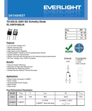
1. Product Overview
EL-SAF01 665JA wani diode ne na Schottky Barrier na Silicon Carbide wanda aka tsara musamman don aikace-aikacen canza wutar lantarki mai inganci da mita mai girma. Na'urar tana amfani da daidaitaccen kunshewar TO-220-2L, tana amfani da kyawawan halaye na kayan Silicon Carbide, don cimma aikin da ya zarce na diode na tushen silicon na gargajiya. Aikin sa na asali shine samar da kwararar wutar lantarki ta hanya daya, tare da ƙarancin asarar sauyawa da cajin dawowa baya, wanda ya sa ya zama zaɓi mai kyau na zamani don wutar lantarki da masu jujjuyawar da ke buƙatar inganci da yawan wutar lantarki.
Babban kasuwar wannan kayan ta haɗa da masu zane da injiniyoyi da ke aiki a cikin wutar lantarki mai sauyawa, tsarin canza hasken rana, wutar lantarki mara katsewa, masu sarrafa tuƙi na injin, da kayan aikin wutar lantarki na cibiyar bayanai. Babban fa'idarsa ita ce goyan bayan ƙirar tsarin da ke da mita mafi girma, wanda zai iya rage girman abubuwan da ba su da ƙarfi (kamar inductor da capacitor), don cimma tanadin farashi da girma na tsarin gaba ɗaya. Bugu da ƙari, ƙarancin juriyar zafi yana rage buƙatun sanyaya, yana taimakawa wajen samar da tsarin sarrafa zafi mai sauƙi da amintacce.
2. In-depth Technical Parameter Analysis
2.1 Electrical Characteristics
Electrical parameters define the operating boundaries and performance of a diode under specific conditions.
- Maximum Repetitive Peak Reverse Voltage:650V. This is the maximum instantaneous voltage the diode can withstand in the reverse bias direction without breaking down. It defines the voltage rating for applications such as 400V AC rectification or boost PFC stages.
- Continuous forward current:16A. This is the maximum average forward current that the device can conduct continuously, typically specified at a case temperature of 25°C. Derating is required at higher ambient temperatures.
- Forward voltage:At IF=16A, Tj=25°C, the typical value is 1.5V, and the maximum value is 1.85V. This parameter is crucial for calculating conduction losses. The datasheet also specifies the VF value at the maximum junction temperature, which is typically higher and is very important for worst-case loss calculations.
- Reverse current:Extremely low leakage current, with a typical value of 2µA at VR=520V, Tj=25°C. Even at high temperatures, its leakage current remains at a manageable level. Low leakage current minimizes standby power consumption.
- Total capacitive charge:This is a key parameter for silicon carbide Schottky diodes, with a typical value of 22nC at VR=400V. Unlike conventional diodes, silicon carbide Schottky diodes have no minority carrier storage, so their switching losses are primarily capacitive. QC represents the charge that must be supplied/released per switching cycle, directly impacting switching losses. This low value enables high-frequency operation.
2.2 Thermal Characteristics
Thermal management is crucial for reliability and performance.
- Junction-to-case thermal resistance:Typical value is 1.3°C/W. This low value indicates high efficiency of heat transfer from the semiconductor junction to the package case. It allows for effective removal of heat generated by power dissipation through a heatsink attached to the case.
- Maximum junction temperature:175°C. This is the absolute maximum temperature that a silicon carbide junction can reach. Operating near this limit reduces long-term reliability, so it is recommended to design with a margin.
- Total Power Dissipation:115W at Tc=25°C. This is the maximum power the device can dissipate under ideal cooling conditions. In practical applications, the allowable dissipation power is lower and depends on the heat sink's ability to keep the case temperature low.
2.3 Maximum Ratings and Robustness
These ratings define the absolute limits beyond which permanent damage may occur.
- Surge non-repetitive forward current:56A for a 10ms half-sine wave. This rating indicates the diode's ability to withstand short-circuit or surge current events and is a key factor for reliability under fault conditions.
- Storage Temperature Range:-55°C to +175°C. Defines the safe temperature range for the device when it is not powered.
- Installation Torque:For M3 or 6-32 screws, it is 0.8 to 8.8 N·m. Proper torque is crucial for good thermal contact between the package heatsink and the heat sink.
3. Performance Curve Analysis
The datasheet provides several graphical representations of device behavior, which are crucial for detailed design.
- Forward Voltage - Forward Current Characteristic:This graph shows the relationship between forward voltage and forward current at different junction temperatures. It is used to accurately calculate conduction losses at various operating points, not just the single data point given in the table. The curve typically shows that for a given current, VF decreases slightly as temperature increases, which is characteristic of Schottky diodes.
- Reverse Voltage - Reverse Current Characteristic:The relationship between reverse leakage current and reverse voltage is plotted, typically at multiple temperatures. It helps designers understand off-state losses and ensures that the leakage current at the application's maximum voltage and temperature is acceptable.
- Reverse Voltage - Junction Capacitance Characteristic:Show how the junction capacitance of a diode varies with reverse voltage. Capacitance decreases as reverse voltage increases. This graph is crucial for modeling capacitive switching behavior and calculating QC at specific operating voltages.
- Maximum Forward Current vs. Case Temperature Characteristic:Illustrates how the maximum allowable continuous forward current must be derated as case temperature increases. This is the primary chart for thermal design, determining the required heatsink performance.
- Power Dissipation vs. Case Temperature:Similar to current derating, this shows how the maximum allowable power dissipation decreases as the case temperature rises.
- Surge Current - Pulse Width Characteristic:It details the surge current capability for pulse widths other than the standard 10ms. It allows for assessing survivability under various transient conditions.
- Stored Capacitor Energy vs. Reverse Voltage Characteristic:The relationship between stored capacitor energy and reverse voltage is plotted. Switching loss energy can be derived from this.
- Transient Thermal Impedance vs. Pulse Width Relationship:It is crucial for evaluating temperature rise during short power pulses. The thermal impedance of a single short pulse is lower than the steady-state junction-to-case thermal resistance, allowing higher instantaneous power without overheating the junction.
4. Mechanical and Packaging Information
4.1 Package Outline and Dimensions
The device adopts the industry-standard TO-220-2L package. Key dimensions in the datasheet include:
- Overall length: 15.6 mm
- 总宽度:9.99 mm总高度:4.5 mm
- Pin pitch: 5.08 mm
- Mounting hole distance: 8.70 mm
- Provides heat sink dimensions and lead forming details to facilitate mechanical integration and PCB pad design.
4.2 Pin Configuration and Polarity
Pin definitions are clear:
- Pin 1:Cathode.
- Pin 2:Anode.
- Case:The metal heatsink is electrically connected to the cathode. This connection is critical for safety and design: the heatsink will be at cathode potential, so it must be isolated if other parts of the circuit are at a different potential. An appropriate insulation kit must be used.
4.3 Recommended PCB Pad Layout
A surface-mount lead-formed pad layout is recommended for PCB design. This ensures good solder joint formation and mechanical stability when the device is mounted on the PCB, typically in conjunction with a heatsink.
5. Welding and Assembly Guide
Although the provided excerpt does not contain detailed reflow soldering curves, the general guidelines applicable to TO-220 packaged power devices are as follows:
- Operation:Pay attention to electrostatic discharge protection measures, as silicon carbide devices may be relatively sensitive.
- Soldering:For through-hole mounting of pins, standard wave soldering or manual soldering techniques can be used. The package body temperature should not exceed the maximum storage temperature for an extended period. For surface-mount pin forming, follow the standard reflow soldering profile for lead-free components.
- Heat sink installation:
- Ensure the mounting surfaces of the radiator and diode heat sink are clean, flat, and free of burrs.
- Apply a thin, even layer of thermal interface material to improve heat transfer.
- If electrical isolation is required, use insulating washers and screws with shoulder washers. Apply thermal grease on both sides of the insulator.
- Secure the diode using the specified mounting torque with M3 or 6-32 screws and nuts. Avoid over-tightening to prevent damage to the package or stripped threads.
- Storage:Store in a dry, anti-static environment within the specified temperature range.
6. Application Recommendations
6.1 Typical Application Circuit
- Power Factor Correction Boost Diode:In continuous conduction mode boost PFC circuits, the diode's low QC and fast switching are crucial for achieving high efficiency at high switching frequencies. It withstands high voltage stress when the main switch is on.
- Solar Microinverter Output Stage:Used in high-frequency inverter bridges or as freewheeling diodes. Their high-temperature capability suits the demanding environmental conditions of solar applications.
- Uninterruptible Power Supply Inverter/Converter:Acts as freewheeling or clamping diodes in DC-AC inverter or DC-DC converter stages, improving overall system efficiency.
- Motor drive DC bus clamping/freewheeling diode:By clamping the inductive energy from the motor windings, it protects IGBTs or MOSFETs from voltage spikes.
6.2 Key Design Considerations
- Buffer circuit:Due to the extremely fast switching speed and low QC, parasitic inductance in the circuit can cause significant voltage overshoot. It is crucial to carefully design the PCB layout to minimize loop area. It may be necessary to use an RC snubber circuit across the diode to suppress ringing.
- Thermal design:Calculate total power loss. Use maximum junction temperature, junction-to-case thermal resistance, and estimated heatsink thermal resistance to ensure junction temperature remains within safe margin.
- Parallel operation:The datasheet indicates that the device can be used in parallel without thermal runaway. This is due to the positive temperature coefficient of forward voltage at high currents, which promotes current sharing. However, for optimal current sharing, ensure symmetrical layout and use separate gate resistors when driving the associated switches.
- Voltage derating:To enhance long-term reliability, especially in high-temperature or high-reliability applications, derating of the operating reverse voltage should be considered.
7. Technical Comparison and Advantages
Compared to standard silicon fast recovery diodes or even ultrafast recovery diodes, the EL-SAF01 665JA offers significant advantages:
- Essentially zero reverse recovery charge:Silicon diodes have significant Qrr due to minority carrier storage, leading to large current spikes and losses during turn-off. Silicon carbide Schottky diodes are majority carrier devices, so Qrr is negligible. Switching losses are purely capacitive and much lower than Qrr-based losses.
- Higher operating temperature:The wide bandgap of silicon carbide allows a maximum junction temperature of 175°C, compared to 150°C or 125°C for many silicon diodes, enabling operation in hotter environments or with smaller heat sinks.
- Higher switching frequency capability:The combination of low QC and no Qrr makes efficient operation at frequencies well above 100 kHz possible, allowing for a significant reduction in magnetic components.
- Lower forward voltage at high temperatures:Although the VF at room temperature may be comparable to that of silicon Schottky diodes, the VF of silicon carbide Schottky diodes increases less with rising temperature, resulting in better high-temperature conduction performance.
8. Frequently Asked Questions
8.1 Based on Technical Parameters
Q: QC is 22nC. How to calculate switching loss?
A: The energy loss per switching cycle is approximately E_sw ≈ 0.5 * QC * V, where V is the reverse voltage withstand during turn-off. For example, at 400V, E_sw ≈ 0.5 * 22nC * 400V = 4.4µJ. Multiply by the switching frequency to obtain the power loss: P_sw = E_sw * f_sw. At 100 kHz, P_sw ≈ 0.44W.
Q: Why is the case connected to the cathode? Is isolation always required?
A: For thermal and mechanical reasons, the internal die is mounted on a substrate that is electrically connected to the cathode heat sink tab. Isolation is required if the heat sink is at a different potential than the cathode in the circuit. If the cathode is grounded and the heat sink is also grounded, isolation may not be necessary, but it is often used as a safety best practice.
Q: Can I directly replace a silicon diode with this diode in an existing circuit?
A: Direct replacement without review is not possible. Although voltage and current ratings may match, the extremely fast switching speed can cause severe voltage overshoot and electromagnetic interference due to circuit parasitics, which are not issues for slower silicon diodes. PCB layout and snubber circuit design must be re-evaluated.
9. Practical Design and Application Cases
Case Study: High-Density 2kW Server Power Supply PFC Stage.A designer replaced a 600V/15A silicon ultrafast diode with an EL-SAF01 in an 80kHz CCM boost PFC. Calculations show the silicon carbide diode reduces switching losses by approximately 60% and slightly improves conduction loss. The 0.86W loss saved per diode allows the switching frequency to be increased to 140kHz, reducing the boost inductor size by about 40% and meeting the goal of higher power density. The existing heatsink remains sufficient due to the lower total losses.
Case Study: Solar Microinverter H-Bridge.In a 300W microinverter, four EL-SAF01 diodes are used as freewheeling diodes for the H-bridge MOSFETs. Their high-temperature rating ensures reliability in rooftop environments where enclosure temperatures can exceed 70°C. Low QC minimizes losses at high switching frequencies, contributing to higher overall conversion efficiency, which is crucial for solar harvesting.
10. Working Principle
A Schottky diode is formed by a metal-semiconductor junction, which is different from a standard PN junction diode. The EL-SAF01 uses silicon carbide as the semiconductor. The Schottky barrier formed at the metal-SiC interface allows only majority carrier conduction. When forward-biased, electrons are injected from the semiconductor into the metal, allowing current to flow with a relatively low forward voltage drop. When reverse-biased, the Schottky barrier prevents current flow. The key difference from a PN diode is the absence of minority carrier injection and storage. This means there is no diffusion capacitance associated with stored charge in the drift region, resulting in the "zero reverse recovery" characteristic. The only capacitance is the junction depletion layer capacitance, which is voltage-dependent and gives rise to a measurable QC. The wide bandgap of silicon carbide provides a high breakdown field strength, enabling a 650V rating in a relatively small chip size, and its high thermal conductivity aids in heat dissipation.
11. Technology Trends
Silicon carbide power devices, including Schottky diodes and MOSFETs, represent a significant trend in power electronics toward higher efficiency, frequency, and power density. The market is shifting from 600-650V devices to higher voltage ratings, while the increase in wafer size and improvement in manufacturing yield are driving another trend of lower cost per ampere. Integration is another trend, with modules combining silicon carbide MOSFETs and Schottky diodes emerging. Furthermore, research continues to improve the Schottky barrier interface to further reduce forward voltage drop and enhance reliability. Globally, energy efficiency standards and the electrification of transportation and renewable energy systems are driving the adoption of silicon carbide.
Detailed Explanation of LED Specification Terminology
Complete Explanation of LED Technical Terminology
I. Core Indicators of Photoelectric Performance
| Terminology | Unit/Representation | Popular Explanation | Why It Is Important |
|---|---|---|---|
| Luminous Efficacy | lm/W (lumens per watt) | The luminous flux emitted per watt of electrical energy, the higher the more energy-efficient. | Directly determines the energy efficiency grade and electricity cost of the luminaire. |
| Luminous Flux | lm (lumen) | The total amount of light emitted by a light source, commonly known as "brightness". | Determine if the lamp is bright enough. |
| Viewing Angle | ° (degrees), such as 120° | The angle at which light intensity drops to half, determining the beam's width. | Affects the illumination range and uniformity. |
| Color Temperature (CCT) | K (Kelvin), e.g., 2700K/6500K | The warmth or coolness of light color; lower values are yellowish/warm, higher values are whitish/cool. | Determines the lighting atmosphere and suitable application scenarios. |
| Color Rendering Index (CRI / Ra) | No unit, 0–100 | The ability of a light source to reproduce the true colors of objects, Ra≥80 is recommended. | Affects color fidelity, used in high-demand places such as shopping malls and art galleries. |
| Color Tolerance (SDCM) | MacAdam Ellipse Steps, e.g., "5-step" | Quantitative indicator of color consistency, the smaller the step number, the more consistent the color. | Ensure no color difference among the same batch of luminaires. |
| Dominant Wavelength | nm (nanometer), e.g., 620nm (red) | The wavelength value corresponding to the color of a colored LED. | Determine the hue of monochromatic LEDs such as red, yellow, and green. |
| Spectral Distribution | Wavelength vs. Intensity Curve | Shows the intensity distribution of light emitted by an LED across various wavelengths. | Affects color rendering and color quality. |
II. Electrical Parameters
| Terminology | Symbols | Popular Explanation | Design Considerations |
|---|---|---|---|
| Forward Voltage | Vf | Minimum voltage required to turn on an LED, similar to a "starting threshold". | The driving power supply voltage must be ≥ Vf, and the voltage adds up when multiple LEDs are connected in series. |
| Forward Current | If | The current value that allows the LED to emit light normally. | Constant current drive is commonly used, where the current determines brightness and lifespan. |
| Maximum Pulse Current | Ifp | Peak current that can be withstood in a short time, used for dimming or flashing. | Pulse width and duty cycle must be strictly controlled, otherwise overheating damage will occur. |
| Reverse Voltage | Vr | The maximum reverse voltage that an LED can withstand; exceeding it may cause breakdown. | A cikin da'ira, ya kamata a hana haɗin baya ko kuma ƙarfin lantarki mai ƙarfi. |
| Thermal Resistance | Rth(°C/W) | The resistance to heat flow from the chip to the solder joint. A lower value indicates better heat dissipation. | High thermal resistance requires a more robust heat dissipation design; otherwise, the junction temperature will increase. |
| Electrostatic Discharge Immunity (ESD Immunity) | V (HBM), such as 1000V | Anti-static strike capability, the higher the value, the less susceptible to damage from static electricity. | Anti-static measures must be implemented during production, especially for high-sensitivity LEDs. |
III. Thermal Management and Reliability
| Terminology | Key Indicators | Popular Explanation | Impact |
|---|---|---|---|
| Junction Temperature | Tj (°C) | The actual operating temperature inside the LED chip. | For every 10°C reduction, the lifespan may double; excessively high temperatures cause lumen depreciation and color shift. |
| Lumen Depreciation | L70 / L80 (hours) | The time required for brightness to drop to 70% or 80% of its initial value. | Directly defines the "useful life" of an LED. |
| Lumen Maintenance | % (e.g., 70%) | Percentage of remaining brightness after a period of use. | Characterizes the ability to maintain brightness after long-term use. |
| Color Shift | Δu′v′ or MacAdam Ellipse | The degree of color change during use. | Affects the color consistency of the lighting scene. |
| Thermal Aging | Material performance degradation | Degradation of packaging materials due to long-term high temperature. | May lead to decreased brightness, color shift, or open-circuit failure. |
IV. Encapsulation and Materials
| Terminology | Common Types | Popular Explanation | Characteristics and Applications |
|---|---|---|---|
| Package Type | EMC, PPA, Ceramic | The housing material that protects the chip and provides optical and thermal interfaces. | EMC has good heat resistance and low cost; ceramic has excellent heat dissipation and long lifespan. |
| Chip structure | Front-side, Flip Chip | Chip Electrode Layout. | Flip-chip provides better heat dissipation and higher luminous efficacy, suitable for high-power applications. |
| Phosphor coating | YAG, silicate, nitride | Covered on the blue light chip, partially converted into yellow/red light, mixed into white light. | Different phosphors affect luminous efficacy, color temperature, and color rendering. |
| Lens/Optical Design | Flat, Microlens, Total Internal Reflection | Optical structure on the encapsulation surface, controlling light distribution. | Determines the emission angle and light distribution curve. |
V. Quality Control and Binning
| Terminology | Grading Content | Popular Explanation | Purpose |
|---|---|---|---|
| Luminous Flux Grading | Codes such as 2G, 2H | Grouped by brightness level, each group has a minimum/maximum lumen value. | Ensure uniform brightness for products within the same batch. |
| Voltage binning | Codes such as 6W, 6X | Grouped by forward voltage range. | Facilitates driver power matching and improves system efficiency. |
| Color Grading | 5-step MacAdam Ellipse | Group by color coordinates to ensure colors fall within a minimal range. | Ensure color consistency to avoid uneven colors within the same luminaire. |
| Color temperature binning | 2700K, 3000K, etc. | Grouped by color temperature, each group has a corresponding coordinate range. | To meet the color temperature requirements of different scenarios. |
VI. Testing and Certification
| Terminology | Standard/Test | Popular Explanation | Meaning |
|---|---|---|---|
| LM-80 | Lumen Maintenance Test | Long-term illumination under constant temperature conditions, recording brightness attenuation data. | Used to estimate LED lifespan (combined with TM-21). |
| TM-21 | Standard for Lifetime Projection | Projecting lifetime under actual use conditions based on LM-80 data. | Provide scientific life prediction. |
| IESNA standard | Standard of the Illuminating Engineering Society | Covers optical, electrical, and thermal testing methods. | Industry-recognized testing basis. |
| RoHS / REACH | Environmental certification | Ensure the product does not contain harmful substances (e.g., lead, mercury). | Entry requirements for the international market. |
| ENERGY STAR / DLC | Energy Efficiency Certification | Energy efficiency and performance certification for lighting products. | Yawan da ake amfani da shi a cikin sayayyar gwamnati da ayyukan tallafi, don haɓaka gasar kasuwa. |