Table of Contents
- 1. Product Overview
- 2. In-depth Technical Parameter Analysis
- 2.1 Absolute Maximum Ratings
- 2.2 Electrical Characteristics
- 2.3 Thermal Characteristics
- 3. Performance Curve Analysis
- 3.1 VF-IF Characteristic Curve
- 3.2 VR-IR Characteristic Curve
- 3.3 VR-Ct Characteristic Curve
- 3.4 Maximum Forward Current vs. Case Temperature Relationship
- 3.5 Transient Thermal Impedance
- 4. Mechanical and Package Information
- 4.1 Pin Configuration and Polarity
- 4.2 Package Dimensions and Outline Drawing
- 4.3 Recommended PCB Land Pattern
- 5. Assembly and Operation Guide
- 5.1 Installation Torque
- 5.2 Storage Conditions
- 6. Application Recommendations
- 6.1 Typical Application Circuit
- 6.2 Key Design Considerations
- 7. Technical Comparison and Advantages
- 8. Frequently Asked Questions
- 8.1 What does "virtually no switching loss" specifically refer to?
- 8.2 Why is the case connected to the cathode?
- 8.3 Yaya ake lissafin asarar wutar wannan diode?
- 8.4 Shin za a iya maye gurbin silicon diode kai tsaye da wannan diode?
- 9. Design Application Case Study
- 10. Introduction to Working Principle
- 11. Technology Development Trends
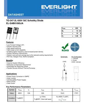
1. Product Overview
This document details the specifications of a high-performance silicon carbide Schottky barrier diode in a TO-247-2L package. The device is designed for power electronics applications demanding high efficiency, high-frequency operation, and superior thermal performance. Its core function is to provide unidirectional current conduction while exhibiting extremely low switching losses and reverse recovery charge, a significant advantage over traditional silicon PN junction diodes.
The primary positioning of this component is for application in advanced power conversion systems where efficiency and power density are critical. Its core advantages stem from the fundamental properties of silicon carbide material, enabling operation at higher temperatures, voltages, and switching frequencies than silicon-based devices. Target markets include industrial power supplies, renewable energy systems, and motor drive applications, where these characteristics translate directly into system-level benefits.
2. In-depth Technical Parameter Analysis
2.1 Absolute Maximum Ratings
Absolute maximum ratings define the stress limits that may cause permanent damage to the device. These values are not intended for normal operation.
- Repetitive peak reverse voltage:650V. This is the maximum instantaneous reverse voltage that can be applied repeatedly.
- Continuous Forward Current:10A. This is the maximum direct current that the diode can continuously conduct under the limitations of maximum junction temperature and thermal resistance.
- Non-repetitive Surge Current:30A. This rating indicates the diode's ability to withstand a single high-current overload event (10ms sine half-wave) without failure, which is crucial for handling inrush currents or fault conditions.
- Junction Temperature:175°C. The maximum allowable temperature of the semiconductor junction itself.
- Storage Temperature:-55°C to +175°C.
2.2 Electrical Characteristics
These parameters define the performance of the device under specified test conditions.
- Forward Voltage:Under the conditions of IF=10A, TJ=25°C, the typical value is 1.48V, and the maximum value is 1.85V. This low VF is a key characteristic of SiC Schottky diodes, contributing to reduced conduction losses. Please note that VF increases with temperature, reaching approximately 1.9V at TJ=175°C.
- Reverse Leakage Current:Under the conditions of VR=520V and TJ=25°C, the typical value is 2µA, and the maximum value is 60µA. The leakage current increases with rising temperature, a characteristic that must be considered in high-temperature design.
- Total capacitive charge:Under the condition of VR=400V, the typical value is 15nC. This is a key parameter for calculating switching losses. A low QC value means that the energy stored in the diode's junction capacitance is very small, and this energy must be dissipated in each switching cycle, thereby achieving the "virtually no switching loss" advantage as described.
- Energy stored in capacitor:Under the condition of VR=400V, the typical value is 2.2µJ. This is the energy stored in the diode capacitance at the specified voltage and is directly related to QC.
2.3 Thermal Characteristics
Thermal management is crucial for reliable operation and achieving rated performance.
- Junction-to-case thermal resistance:The typical value is 1.7°C/W. This low value indicates excellent heat transfer performance from the semiconductor chip to the device case, allowing heat to be efficiently removed via a heatsink attached to the case. At TC=25°C, the total power dissipation rating of 88W is derived from this parameter and the maximum junction temperature.
3. Performance Curve Analysis
The datasheet contains multiple characteristic curves that are crucial for design engineers.
3.1 VF-IF Characteristic Curve
This graph plots the relationship between forward voltage and forward current, typically at multiple junction temperatures (e.g., 25°C and 175°C). It visually demonstrates the low forward voltage drop and its positive temperature coefficient. The positive temperature coefficient is a beneficial characteristic for parallel operation, as it promotes current sharing and prevents thermal runaway.
3.2 VR-IR Characteristic Curve
This curve shows the relationship between reverse voltage and reverse leakage current, also at different temperatures. It emphasizes how the leakage current remains relatively low before approaching the breakdown region and how it increases exponentially with temperature.
3.3 VR-Ct Characteristic Curve
This figure illustrates how the total capacitance of a diode decreases with increasing reverse bias voltage. This nonlinear capacitance is a key factor in high-frequency switching behavior.
3.4 Maximum Forward Current vs. Case Temperature Relationship
This derating curve shows how the maximum allowable continuous forward current decreases with increasing case temperature. It is a key tool for determining the required heat sink performance for a specific application current.
3.5 Transient Thermal Impedance
The curve of transient thermal resistance versus pulse width is crucial for evaluating thermal performance under pulsed current conditions. It indicates that for very short pulses, the effective thermal resistance is lower than the steady-state junction-to-case thermal resistance, thereby allowing higher peak currents.
4. Mechanical and Package Information
4.1 Pin Configuration and Polarity
The device is housed in a TO-247-2L package with two pins. Pin 1 is the cathode, and pin 2 is the anode. Importantly, the metal mounting tab or case of the package is electrically connected to the cathode. This must be carefully considered during installation to prevent short circuits, as the case must be insulated from the heatsink unless the heatsink is at cathode potential.
4.2 Package Dimensions and Outline Drawing
Detailed mechanical drawings are provided, with all critical dimensions in millimeters. This includes overall length, width, height, lead pitch, lead diameter, and the dimensions of the mounting holes on the mounting pad. Adherence to these dimensions is necessary for proper PCB pad design and mechanical assembly.
4.3 Recommended PCB Land Pattern
Contains recommended pad layout for surface mounting of leads (after forming), specifying pad dimensions, shape, and spacing to ensure reliable soldering and mechanical strength.
5. Assembly and Operation Guide
5.1 Installation Torque
The specified installation torque for screws used to secure the device to a heatsink is 8.8 N·m (or equivalent lbf-in), applicable to M3 or 6-32 screws. Applying the correct torque ensures optimal thermal contact without damaging the package.
5.2 Storage Conditions
The device should be stored in a dry, non-corrosive environment within the specified storage temperature range of -55°C to +175°C. Standard ESD (Electrostatic Discharge) precautions should be observed during handling, as the Schottky barrier is sensitive to electrostatic damage.
6. Application Recommendations
6.1 Typical Application Circuit
- Power Factor Correction:Used as a boost diode in continuous conduction mode PFC circuits. Its fast switching and low QC minimize turn-off losses, allowing for higher switching frequencies, thereby reducing the size of magnetic components.
- Solar inverter:Applied in the boost stage or within the inverter bridge. High efficiency reduces power loss, and high-temperature capability improves reliability in outdoor environments.
- Motor drive:The position of the freewheeling or clamping diode in the inverter bridge used to drive the motor. The absence of reverse recovery current reduces voltage spikes and electromagnetic interference, and improves the efficiency of the drive.
- Uninterruptible Power Supply and Data Center Power:The aforementioned advantages are equally applicable in the high-density, high-efficiency power conversion stages of these systems.
6.2 Key Design Considerations
- Heat Dissipation:Due to its high power handling capability, an appropriate heat sink must be used when operating at high currents. The thermal resistance from the case to the ambient provided by the heat sink must be calculated based on the maximum ambient temperature, power dissipation, and the desired junction temperature margin.
- Device Parallel Connection:The positive temperature coefficient of VF is beneficial for current sharing when multiple diodes are connected in parallel. However, careful layout is still recommended to ensure symmetrical parasitic inductance and resistance, thereby achieving optimal current sharing.
- Snubber Circuit:Although this diode has essentially no reverse recovery, circuit parasitic inductance can still cause voltage overshoot during turn-off. In applications with extremely high di/dt, the use of a snubber circuit or careful layout may be necessary to minimize loop inductance.
- Gate Drive Considerations:The fast switching of this diode can lead to high di/dt and dv/dt, which may cause noise coupling into the gate drive circuit. Proper shielding and gate drive layout are crucial.
7. Technical Comparison and Advantages
Compared to standard silicon fast recovery diodes and even silicon carbide junction barrier Schottky diodes, this silicon carbide Schottky diode offers the following significant advantages:
- Zero reverse recovery:The Schottky barrier is a majority carrier device, eliminating the minority carrier storage time and the associated reverse recovery current and losses present in PN junction diodes. This is its most notable advantage.
- Higher Operating Temperature:Silicon Carbide material allows a maximum junction temperature of 175°C, higher than typical silicon diodes, enabling operation in harsher environments or with smaller heat sinks.
- Lower Forward Voltage Drop:A cikin yanayin aiki na yau da kullun, VF ɗinsa ya yi ƙasa da silicon fast recovery diode na matakin wutar lantarki iri ɗaya, don haka ya rage asarar kunnawa.
- Ƙarfin saurin saurin sauyawa mafi girma:Haɗin ƙaramin QC da rashin Qrr yana ba shi damar yin aiki cikin inganci a cikin mitoci mafi girma, wanda kai tsaye ke haifar da ƙaramin girman abubuwan da ba su da ƙarfi (inductors, capacitors), da ƙarfin ƙarfi mafi girma.
8. Frequently Asked Questions
8.1 What does "virtually no switching loss" specifically refer to?
It refers to negligible reverse recovery loss. Although capacitive switching loss still exists, the total switching loss is significantly reduced, typically by an order of magnitude, due to the complete absence of the much larger reverse recovery loss commonly found in silicon diodes.
8.2 Why is the case connected to the cathode?
This is a common design in power packages, aimed at simplifying internal connections and improving thermal performance. This means the heatsink must be electrically isolated from the rest of the system unless it is intentionally kept at cathode potential. Insulating spacers and thermal interface materials with high dielectric strength are required.
8.3 Yaya ake lissafin asarar wutar wannan diode?
Total power loss is the sum of conduction loss and switching loss. Conduction loss = IF(AVG) * VF. Switching loss ≈ (1/2) * C * V^2 * f (for capacitive loss), where C is the effective capacitance, V is the blocking voltage, and f is the switching frequency. The Qrr loss component is zero.
8.4 Shin za a iya maye gurbin silicon diode kai tsaye da wannan diode?
Regarding voltage and current ratings, it is generally acceptable. However, faster switching speeds may expose circuit parasitic parameters, potentially leading to higher voltage spikes. The gate drive of related switching devices (e.g., MOSFETs) may require re-evaluation for its noise immunity. Due to different loss characteristics, the thermal design should also be re-evaluated.
9. Design Application Case Study
Scenario:Upgrade the silicon ultrafast diode in a 2kW continuous conduction mode power factor correction boost stage to this silicon carbide Schottky diode. The original design operates at a frequency of 100kHz.
Analysis:The original silicon diode has a Qrr of 50nC and a VF of 1.8V. Switching losses are significant. By replacing it with this silicon carbide diode, the following improvements were achieved:
- Switching loss reduction:Qrr loss is eliminated. Capacitive switching loss is also reduced due to lower QC.
- Conduction loss reduction:For the same average current, the lower VF reduces conduction loss by approximately 18%.
- Frequency scaling potential:The significant reduction in total switching loss enables designers toincrease the switching frequencyto 200-300kHz. This reduces the size and weight of the boost inductor and EMI filter components by nearly 50%, directly achieving "power density improvement".
- Thermal Management:The total power loss of the diode is lower. Combined with its higher junction temperature rating, this can allow for a reduction in heat sink size, further saving cost and space.
Result:System full-load efficiency increases by 1-2%, power density increases, and system cost may be reduced due to smaller magnetic components and cooling systems.
10. Introduction to Working Principle
Schottky diode yana samuwa daga haɗin ƙarfe da semiconductor, wanda ya bambanta da haɗin P-N semiconductor na diode na yau da kullun. A cikin wannan Schottky diode na silicon carbide, lambar ƙarfe tana haɗuwa kai tsaye da silicon carbide na nau'in-n. Wannan yana haifar da shingen Schottky, wanda ke ba da damar kwarara na halin yanzu cikin sauƙi a cikin alkiblar gaba lokacin da ake amfani da ƙarfin lantarki mai kyau akan ƙarfe idan aka kwatanta da semiconductor.
Babban bambancin aiki yana cikin dawowar baya. A cikin diode na PN, kashe shi yana buƙatar cire ƴan ƙananan masu ɗaukar kaya da aka adana (wanda ake kira tsarin dawowar baya), wanda ke ɗaukar lokaci kuma yana haifar da ƙaramin bugun halin yanzu na baya. A cikin Schottky diode, halin yanzu yana ɗauke da mafi yawan masu ɗaukar kaya kawai (electrons a cikin silicon carbide na nau'in-n). Lokacin da ƙarfin lantarki ya koma baya, waɗannan masu ɗaukar kaya suna sharewa kusan nan take, wanda ke haifar da rashin lokacin adana ƴan ƙananan masu ɗaukar kaya, don haka ya haifar da "dawowar baya sifili". Wannan ainihin ka'idar ita ce ainihin dalilin da yasa ake samun saurin sauyawa da ƙananan asarar sauyawa.
11. Technology Development Trends
Silicon carbide power devices represent a major trend in the field of power electronics, driving the transition from traditional silicon-based devices. The market drivers are the global push for higher energy efficiency, higher power density, and the electrification of transportation and industry.
The development of silicon carbide Schottky diodes focuses on several key areas: further reducing specific on-resistance (thereby lowering VF), improving the reliability and stability of the Schottky metal-semiconductor interface at high temperatures, increasing voltage ratings to 1.2kV, 1.7kV and above to meet medium-voltage application demands, and reducing device capacitance to support switching frequencies in the MHz range. Integration is another trend, co-packaging silicon carbide Schottky diodes with silicon carbide MOSFETs into modules to create efficient, fast-switching power stages. With increasing manufacturing volumes and decreasing costs, silicon carbide technology is steadily moving from high-end applications to mainstream power conversion products.
Detailed Explanation of LED Specification Terminology
Complete Explanation of LED Technical Terminology
I. Core Indicators of Photoelectric Performance
| Terminology | Unit/Representation | Popular Explanation | Why It Matters |
|---|---|---|---|
| Luminous Efficacy | lm/W | The luminous flux emitted per watt of electrical power, higher values indicate greater energy efficiency. | Directly determines the energy efficiency rating and electricity cost of the lighting fixture. |
| Luminous Flux | lm (Lumen) | Total light output from a light source, commonly known as "brightness". | Determines if a luminaire is bright enough. |
| Viewing Angle | ° (degrees), e.g., 120° | The angle at which luminous intensity drops to half, determining the width of the light beam. | Affects the illumination range and uniformity. |
| Color Temperature (CCT) | K (Kelvin), such as 2700K/6500K | The color temperature of light, lower values are yellowish/warm, higher values are whitish/cool. | Determines the lighting ambiance and suitable application scenarios. |
| Color Rendering Index (CRI / Ra) | Unitless, 0–100 | The ability of a light source to restore the true color of an object, Ra≥80 is recommended. | Affects color authenticity, used in high-demand places such as shopping malls and art galleries. |
| Color tolerance (SDCM) | MacAdam ellipse steps, e.g., "5-step" | A quantitative metric for color consistency; a smaller step number indicates better color consistency. | Ensure no color variation among luminaires from the same batch. |
| Dominant Wavelength | nm (nanometer), e.g., 620nm (red) | Rangi ya LED ya rangi inayolingana na thamani ya urefu wa wimbi. | Inaamua rangi ya LED moja kama nyekundu, manjano, kijani, n.k. |
| Spectral Distribution | Wavelength vs. Intensity Curve | Shows the intensity distribution of light emitted by an LED at each wavelength. | Affects color rendering and color quality. |
II. Electrical Parameters
| Terminology | Symbol | Popular Explanation | Design Considerations |
|---|---|---|---|
| Forward Voltage | Vf | The minimum voltage required to light up an LED, similar to a "starting threshold". | The driving power supply voltage must be ≥ Vf, and the voltage accumulates when multiple LEDs are connected in series. |
| Forward Current | If | The current value that makes the LED emit light normally. | Constant current drive is often used, as the current determines brightness and lifespan. |
| Maximum Pulse Current (Pulse Current) | Ifp | Peak current that can be withstood for a short period, used for dimming or flashing. | Pulse width and duty cycle must be strictly controlled to avoid overheating damage. |
| Reverse Voltage | Vr | The maximum reverse voltage that an LED can withstand; exceeding this may cause breakdown. | The circuit must be protected against reverse connection or voltage surges. |
| Thermal Resistance | Rth (°C/W) | The resistance to heat transfer from the chip to the solder joint; a lower value indicates better heat dissipation. | High thermal resistance requires a stronger heat dissipation design; otherwise, the junction temperature will increase. |
| Electrostatic Discharge Immunity (ESD Immunity) | V (HBM), e.g., 1000V | ESD strike resistance, a higher value indicates greater resistance to electrostatic damage. | Anti-static measures must be implemented during production, especially for high-sensitivity LEDs. |
III. Thermal Management and Reliability
| Terminology | Key Indicators | Popular Explanation | Impact |
|---|---|---|---|
| Junction Temperature | Tj (°C) | The actual operating temperature inside the LED chip. | For every 10°C reduction, the lifespan may double; excessively high temperatures lead to lumen depreciation and color shift. |
| Lumen Depreciation | L70 / L80 (hours) | Time required for brightness to drop to 70% or 80% of its initial value. | Directly define the "useful life" of an LED. |
| Lumen Maintenance | % (e.g., 70%) | The percentage of remaining brightness after a period of use. | Characterization of luminance maintenance capability after long-term use. |
| Color Shift | Δu′v′ or MacAdam ellipse | The degree of color change during use. | Affects the color consistency of the lighting scene. |
| Thermal Aging | Material performance degradation | Degradation of packaging materials due to prolonged high temperatures. | May lead to decreased brightness, color shift, or open-circuit failure. |
IV. Packaging and Materials
| Terminology | Common Types | Popular Explanation | Features and Applications |
|---|---|---|---|
| Package Types | EMC, PPA, Ceramic | The housing material that protects the chip and provides optical and thermal interfaces. | EMC has good heat resistance and low cost; ceramic has excellent heat dissipation and long lifespan. |
| Chip structure | Front side, Flip Chip | Chip electrode arrangement method. | Flip Chip offers better heat dissipation and higher luminous efficacy, suitable for high-power applications. |
| Phosphor coating | YAG, silicate, nitride | Coated on the blue LED chip, partially converted to yellow/red light, mixed to form white light. | Different phosphors affect luminous efficacy, color temperature, and color rendering. |
| Lens/Optical Design | Planar, microlens, total internal reflection | Optical structure on the encapsulation surface, controlling light distribution. | Determines the emission angle and light distribution curve. |
V. Quality Control and Binning
| Terminology | Binning Content | Popular Explanation | Purpose |
|---|---|---|---|
| Luminous Flux Binning | Codes such as 2G, 2H | Group by brightness level, each group has a minimum/maximum lumen value. | Ensure consistent brightness for products within the same batch. |
| Voltage binning | Codes such as 6W, 6X | Grouped by forward voltage range. | Facilitates driver power matching and improves system efficiency. |
| Color binning. | 5-step MacAdam ellipse | Group by color coordinates to ensure colors fall within a minimal range. | Ensure color consistency to avoid color unevenness within the same luminaire. |
| Color temperature binning | 2700K, 3000K, etc. | Group by color temperature, each group has a corresponding coordinate range. | Meet the color temperature requirements of different scenarios. |
VI. Testing and Certification
| Terminology | Standard/Test | Popular Explanation | Significance |
|---|---|---|---|
| LM-80 | Lumen Maintenance Test | Long-term operation under constant temperature conditions, recording data on luminance attenuation. | Used for estimating LED lifetime (combined with TM-21). |
| TM-21 | Life Extrapolation Standard | Estimating lifespan under actual use conditions based on LM-80 data. | Providing scientific life prediction. |
| IESNA Standard | Illuminating Engineering Society Standard | Covering optical, electrical, and thermal testing methods. | Industry-recognized testing basis. |
| RoHS / REACH | Environmental Certification | Ensure products are free from hazardous substances (e.g., lead, mercury). | Conditions for market entry into the international market. |
| ENERGY STAR / DLC | Energy efficiency certification. | Energy Efficiency and Performance Certification for Lighting Products. | Commonly used in government procurement and subsidy programs to enhance market competitiveness. |