Table of Contents
- 1. Product Overview
- 2. In-depth Technical Parameter Analysis
- 2.1 Electrical Characteristics
- 2.2 Thermal Characteristics
- 3. Performance Curve Analysis
- 3.1 Forward Characteristics (VF-IF)
- 3.2 Reverse Characteristics and Capacitance
- 3.3 Surge and Transient Performance
- 4. Mechanical and Package Information
- 4.1 Package Outline and Dimensions
- 4.2 Pin Configuration and Polarity Identification
- 5. Soldering and Assembly Guide
- 6. Application Recommendations
- 6.1 Typical Application Circuit
- 6.2 Design Considerations
- 7. Technical Comparison and Advantages
- 8. Frequently Asked Questions (FAQ)
- 9. Practical Design Case Analysis
- 10. Working Principle
- 11. Technology Trends
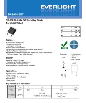
1. Product Overview
This document details the specifications of a high-performance Silicon Carbide Schottky Barrier Diode in a surface-mount TO-252-3L (DPAK) package. The device is designed for high-voltage, high-frequency power conversion applications where high efficiency, high power density, and thermal management are critical. Benefiting from Silicon Carbide technology, this diode offers superior switching characteristics compared to traditional silicon PN-junction diodes, enabling significant system-level performance improvements.
The core advantage of this Silicon Carbide Schottky diode lies in its near-zero reverse recovery charge, which virtually eliminates switching losses associated with diode turn-off. This characteristic is crucial for increasing switching frequencies in power supplies and inverters, thereby allowing the use of smaller passive components such as inductors and capacitors, leading to improved overall power density. The low forward voltage drop further contributes to reduced conduction losses, enhancing system efficiency across the operating temperature range.
2. In-depth Technical Parameter Analysis
2.1 Electrical Characteristics
The device's maximum repetitive peak reverse voltage rating is 650V, making it suitable for universal AC mains applications with ample design margin. Its continuous forward current rating is 20A at a case temperature of 25°C. It is important to note that this current rating is thermally limited and will derate with increasing junction temperature; see the Thermal Characteristics section for details.
For switching diodes, a key performance parameter is the total capacitive charge. This device has a typical Qc of 30nC at a reverse voltage of 400V and a junction temperature of 25°C. This low value confirms minimal stored charge, which directly translates to low switching losses and supports high-frequency operation. The forward voltage drop has a maximum of 1.85V at 25°C conducting 16A, with a typical value rising to 1.9V at the maximum junction temperature of 175°C. The positive temperature coefficient of VF is a beneficial characteristic of silicon carbide Schottky diodes, aiding in current sharing and preventing thermal runaway when multiple devices operate in parallel.
The reverse leakage current is extremely low, with a maximum of only 120µA at 520V and 25°C. This low leakage current contributes to achieving high efficiency, especially under standby or light-load conditions.
2.2 Thermal Characteristics
Effective thermal management is crucial for reliable operation. The primary thermal metric is the junction-to-case thermal resistance, with a typical value of 3.6°C/W. This low value indicates efficient heat transfer from the semiconductor junction to the package case, allowing heat to be effectively dissipated through an external heatsink attached to the heat spreader. The maximum allowable junction temperature is 175°C, and the device can be stored within a temperature range of -55°C to +175°C.
A lokacin da yanayin harsashi ya kasance 25°C, jimlar ƙimar amfani da wutar lantarki ita ce 50W. A aikace-aikace na ainihi, ainihin izinin amfani da wutar lantarki yana buƙatar ƙididdigewa bisa mafi girman zafin jiki, juriyar zafi, da kuma yanayin muhalli. Ana ba da layukan "amfani da wutar lantarki" da "juriya na zafi na ɗan lokaci" don tsara yanayin ɗaukar nauyi na ɗan lokaci da ƙayyadaddun yankin aiki mai aminci.
3. Performance Curve Analysis
3.1 Forward Characteristics (VF-IF)
The VF-IF characteristic curve illustrates the relationship between forward voltage drop and forward current at different junction temperatures. As expected for a Schottky diode, the curve shows a lower knee voltage compared to a silicon PN diode. The curve also demonstrates a positive temperature coefficient, meaning that at a given current, VF increases as Tj rises. This graph is crucial for calculating conduction losses under various operating conditions.
3.2 Reverse Characteristics and Capacitance
VR-IR curve shows extremely low reverse leakage current within the voltage range up to the blocking voltage. VR-Ct curve illustrates the junction capacitance as a function of reverse bias voltage. Capacitance decreases with increasing reverse voltage, which is a characteristic of the depletion region width varying with voltage. Low and voltage-dependent capacitance affects switching speed and Qc parameter.
3.3 Surge and Transient Performance
The "Maximum Ip – TC Characteristic" chart defines the permissible non-repetitive surge current as a function of case temperature. The device can withstand a surge current of 26A at 25°C. The "IFSM – PW Characteristic" graph further details the surge current capability versus pulse width, which is crucial for designing protection against surge currents or fault conditions. The "EC-VR Characteristic" curve plots the stored capacitive energy versus reverse voltage, important for understanding losses in resonant circuits.
4. Mechanical and Package Information
4.1 Package Outline and Dimensions
The device is packaged in TO-252-3L. Key dimensions include: typical overall package length of 6.60mm, typical width of 6.10mm, and typical height of 2.30mm. The basic lead pitch is 2.28mm. A large metal tab serves as the primary thermal path and is electrically connected to the cathode lead. A detailed dimension drawing with tolerances is provided for PCB pad design.
4.2 Pin Configuration and Polarity Identification
The pin configuration is clearly defined: Pin 1 is the cathode, Pin 2 is the anode, and the case is also connected to the cathode. Correct polarity identification during assembly is critical to prevent device failure. A recommended surface-mount PCB pad layout is provided to ensure proper solder joint formation and thermal connection to the board.
5. Soldering and Assembly Guide
As a surface-mount component, this diode is suitable for reflow soldering processes. Although specific reflow profile parameters are not listed in this specification, a lead-free reflow profile compliant with the IPC/JEDEC J-STD-020 standard should be followed. The maximum package body temperature during soldering should not exceed the specified maximum storage temperature of 175°C for an extended period. The installation torque for screws used for the heat sink is specified as 8.8 N·cm.
Preventive measures should be taken to avoid applying mechanical stress to the pins after soldering. The device should be stored in a dry, anti-static environment before use to prevent moisture absorption and electrostatic discharge damage.
6. Application Recommendations
6.1 Typical Application Circuit
This silicon carbide Schottky diode is ideally suited for a variety of high-performance power conversion topologies.
- Power Factor Correction in Switching Power Supplies.Used as a boost diode for continuous conduction mode or critical conduction mode PFC stages. Its fast switching and low Qc reduce switching losses at high line frequencies, improving efficiency, especially at high line voltages.
- Solar inverter:Used in the boost stage of PV microinverters or string inverters to handle high voltage and high current with minimal losses, maximizing energy harvesting.
- Uninterruptible power supply:Used in the inverter output stage or battery charging circuit to achieve efficient high-frequency switching.
- Motor Drive:Can be used for freewheeling or clamping circuits in variable frequency drives to efficiently manage the inductive kickback of the motor.
- Data Center Power Supply:Achieving high efficiency in server power supplies is crucial, where reducing each percentage point of loss is of utmost importance.
6.2 Design Considerations
Thermal Design:The primary design challenge is managing junction temperature. Use the RθJC value and maximum Tj to calculate the required heat dissipation. The metal tab must be soldered to a sufficiently large copper pad on the PCB, possibly connected to inner or backside layers through thermal vias to act as a heat sink. For higher power applications, an external heat sink connected to the tab may be required.
Parallel Operation:VF's positive temperature coefficient is beneficial for current sharing among parallel diodes. However, careful layout symmetry is still required to ensure equal parasitic inductance and resistance in each branch, preventing current imbalance during fast transient processes.
Snubber circuit:Although the diode's reverse recovery charge is extremely low, parasitic circuit inductance and capacitance can still cause voltage overshoot during turn-off. A snubber circuit may be needed to clamp these spikes and ensure reliable operation within the maximum voltage rating.
Gate drive considerations:The fast switching of this diode may lead to high di/dt and dv/dt. This may require attention to the gate drive design of the accompanying switching transistor to avoid false triggering due to the Miller effect or to manage electromagnetic interference.
7. Technical Comparison and Advantages
Compared to standard silicon fast recovery diodes or even silicon carbide junction barrier Schottky diodes, this Schottky diode offers significant advantages:
- Zero reverse recovery:The Schottky barrier mechanism has no minority carrier storage, resulting in near-zero Qc. This eliminates reverse recovery current spikes, reduces switching losses in both the diode itself and the accompanying transistor, and minimizes electromagnetic interference.
- High-temperature operation:The material properties of silicon carbide allow a maximum junction temperature of up to 175°C, which is higher than typical silicon devices, providing greater design margin or allowing the use of smaller heat sinks.
- High Frequency Capability:The combination of low Qc and low capacitance enables efficient operation at switching frequencies up to several hundred kHz, surpassing the practical limitations of silicon fast recovery diodes.
- Efficiency Improvement:Lower VF and the absence of recovery loss directly translate to higher system efficiency, especially under partial load and high line conditions.
8. Frequently Asked Questions (FAQ)
Q: Can this diode directly replace a silicon fast recovery diode in an existing design?
A: While it may be a pin-compatible electrical substitute, a design review is mandatory. Faster switching speeds may exacerbate voltage spikes caused by circuit parasitics. Thermal performance will also differ. Snubber values and thermal management design should be re-evaluated.
Q: Why is the case connected to the cathode? Does this require isolation?
A: Yes, the metal tab is electrically live. The PCB pad it connects to must be on the cathode net. If the tab is connected to an external heatsink, that heatsink must be electrically isolated from other potentials or the system chassis unless the chassis is also at cathode potential.
Q: How is the surge current rating applied?
A: The 26A IFSM rating is for a non-repetitive event. It must not be used to calculate continuous current capability. For other pulse durations, the "IFSM – PW" curve must be consulted.
Q: What is the significance of the capacitor energy storage parameter?
A: In applications such as LLC resonant converters, the output capacitance of the diode discharges during each switching cycle, causing losses. EC quantifies this loss. A lower EC indicates lower capacitive switching losses.
9. Practical Design Case Analysis
Scenario: Design a 1kW PFC stage for a server power supply that complies with the 80 Plus Titanium efficiency standard.
The design employs an interleaved critical conduction mode topology with a switching frequency of 100kHz. Each phase handles 500W. The boost diode must block up to 400VDC and carry a peak current of approximately 10A. Initially, silicon ultrafast diodes were considered, but calculations revealed that recovery-related losses per phase exceeded 5W at high line voltages.
By replacing them with this 650V silicon carbide Schottky diode, the recovery losses are eliminated. The remaining losses are primarily conduction loss and a very small capacitive loss. Thermal calculations indicate that the diode junction temperature rise is manageable. This substitution directly contributes to meeting the Titanium standard's requirement of greater than 96% efficiency at 230VAC input, while also allowing for smaller magnetic components due to the high and clean switching frequency.
10. Working Principle
Schottky diodes are formed by a metal-semiconductor junction, which is different from the p-n semiconductor junction of standard diodes. In this silicon carbide Schottky diode, the metal contact forms a junction with n-type silicon carbide. This creates a Schottky barrier that allows current to flow easily in the forward direction when a positive bias is applied to the metal relative to the semiconductor. Under reverse bias, the barrier widens, preventing current flow.
The key difference is that current transport is dominated primarily by majority carriers. There is no process of minority carrier injection, storage, and subsequent removal as in PN junction diodes. Therefore, when the diode switches from forward conduction to reverse blocking, there is no reverse recovery current spike or associated delay time. The diode turns off almost instantaneously, limited only by the charging of its junction capacitance. This fundamental principle is the source of its high-speed switching performance and low switching losses.
11. Technology Trends
Silicon carbide power devices represent a significant trend in power electronics, enabling higher efficiency, power density, and operating temperatures compared to silicon-based devices. For diodes, the development trends are towards higher voltage ratings, lower forward voltage drop, and smaller capacitance. The TO-252-3L package used here is a mainstay for surface-mount power devices, but there is a concurrent trend towards packages with lower inductance and better thermal performance. Integration is another trend, with co-packaged silicon carbide MOSFET and Schottky diode "half-bridge" modules emerging to minimize parasitic inductance in the switching cell. The ongoing reduction in the cost of silicon carbide substrates is enabling this technology to expand beyond high-end server and telecom power supplies into a broader range of applications.
Detailed Explanation of LED Specification Terminology
Complete Explanation of LED Technical Terminology
I. Core Indicators of Photoelectric Performance
| Terminology | Unit/Representation | Popular Explanation | Why It Matters |
|---|---|---|---|
| Luminous Efficacy | lm/W | The luminous flux emitted per watt of electrical power, the higher the more energy efficient. | Directly determines the energy efficiency rating and electricity cost of the lighting fixture. |
| Luminous Flux | lm (lumen) | Total light output from a light source, commonly known as "brightness". | Determines if a luminaire is bright enough. |
| Viewing Angle | ° (degrees), e.g., 120° | The angle at which luminous intensity drops to half, determining the width of the light beam. | Affects the illumination range and uniformity. |
| Color Temperature (CCT) | K (Kelvin), such as 2700K/6500K | The color temperature of light, lower values are yellowish/warm, higher values are whitish/cool. | Determines the lighting ambiance and suitable application scenarios. |
| Color Rendering Index (CRI / Ra) | Unitless, 0–100 | The ability of a light source to restore the true color of an object, Ra≥80 is recommended. | Affects color authenticity, used in high-demand places such as shopping malls and art galleries. |
| Color tolerance (SDCM) | MacAdam ellipse steps, e.g., "5-step" | A quantitative metric for color consistency; a smaller step number indicates better color consistency. | Ensure no color variation among luminaires from the same batch. |
| Dominant Wavelength | nm (nanometer), e.g., 620nm (red) | Rangi ya LED ya rangi inayolingana na thamani ya urefu wa wimbi. | Inaamua rangi ya LED ya rangi moja kama nyekundu, manjano, kijani, n.k. |
| Spectral Distribution | Wavelength vs. Intensity Curve | Shows the intensity distribution of light emitted by an LED at each wavelength. | Affects color rendering and color quality. |
II. Electrical Parameters
| Terminology | Symbol | Popular Explanation | Design Considerations |
|---|---|---|---|
| Forward Voltage | Vf | The minimum voltage required to light up an LED, similar to a "starting threshold". | The driving power supply voltage must be ≥ Vf, and the voltage accumulates when multiple LEDs are connected in series. |
| Forward Current | If | The current value that makes the LED emit light normally. | Constant current drive is often used, as the current determines brightness and lifespan. |
| Maximum Pulse Current (Pulse Current) | Ifp | Peak current that can be withstood for a short period, used for dimming or flashing. | Pulse width and duty cycle must be strictly controlled to avoid overheating and damage. |
| Reverse Voltage | Vr | The maximum reverse voltage that an LED can withstand; exceeding this may cause breakdown. | The circuit must be protected against reverse connection or voltage surges. |
| Thermal Resistance | Rth (°C/W) | The resistance to heat transfer from the chip to the solder joint; a lower value indicates better heat dissipation. | High thermal resistance requires a stronger heat dissipation design; otherwise, the junction temperature will increase. |
| Electrostatic Discharge Immunity (ESD Immunity) | V (HBM), e.g., 1000V | ESD strike resistance, a higher value indicates greater resistance to electrostatic damage. | Anti-static measures must be implemented during production, especially for high-sensitivity LEDs. |
III. Thermal Management and Reliability
| Terminology | Key Indicators | Popular Explanation | Impact |
|---|---|---|---|
| Junction Temperature | Tj (°C) | The actual operating temperature inside the LED chip. | For every 10°C reduction, the lifespan may double; excessively high temperatures lead to lumen depreciation and color shift. |
| Lumen Depreciation | L70 / L80 (hours) | Time required for brightness to drop to 70% or 80% of its initial value. | Directly define the "useful life" of an LED. |
| Lumen Maintenance | % (e.g., 70%) | The percentage of remaining brightness after a period of use. | Characterization of luminance maintenance capability after long-term use. |
| Color Shift | Δu′v′ or MacAdam ellipse | The degree of color change during use. | Affects the color consistency of the lighting scene. |
| Thermal Aging | Material Performance Degradation | Degradation of packaging materials due to prolonged high temperatures. | May lead to decreased brightness, color shift, or open-circuit failure. |
IV. Packaging and Materials
| Terminology | Common Types | Popular Explanation | Features and Applications |
|---|---|---|---|
| Package Types | EMC, PPA, Ceramic | The housing material that protects the chip and provides optical and thermal interfaces. | EMC has good heat resistance and low cost; ceramic has excellent heat dissipation and long lifespan. |
| Chip structure | Front side, Flip Chip | Chip electrode arrangement method. | Flip Chip offers better heat dissipation and higher luminous efficacy, suitable for high-power applications. |
| Phosphor coating | YAG, silicate, nitride | Coated on the blue LED chip, partially converted to yellow/red light, mixed to form white light. | Different phosphors affect luminous efficacy, color temperature, and color rendering. |
| Lens/Optical Design | Planar, microlens, total internal reflection | Optical structure on the encapsulation surface, controlling light distribution. | Determines the emission angle and light distribution curve. |
V. Quality Control and Binning
| Terminology | Binning Content | Popular Explanation | Purpose |
|---|---|---|---|
| Luminous Flux Binning | Codes such as 2G, 2H | Group by brightness level, each group has a minimum/maximum lumen value. | Ensure consistent brightness for products within the same batch. |
| Voltage binning | Codes such as 6W, 6X | Grouped by forward voltage range. | Facilitates driver power matching and improves system efficiency. |
| Color binning. | 5-step MacAdam ellipse | Group by color coordinates to ensure colors fall within a minimal range. | Ensure color consistency to avoid color unevenness within the same luminaire. |
| Color temperature binning | 2700K, 3000K, etc. | Group by color temperature, each group has a corresponding coordinate range. | Meet the color temperature requirements of different scenarios. |
VI. Testing and Certification
| Terminology | Standard/Test | Popular Explanation | Significance |
|---|---|---|---|
| LM-80 | Lumen Maintenance Test | Long-term operation under constant temperature conditions, recording brightness attenuation data. | Used for estimating LED lifespan (combined with TM-21). |
| TM-21 | Life Extrapolation Standard | Estimating lifespan under actual use conditions based on LM-80 data. | Providing scientific life prediction. |
| IESNA Standard | Illuminating Engineering Society Standard | Covering optical, electrical, and thermal testing methods. | Industry-recognized testing basis. |
| RoHS / REACH | Environmental Certification | Ensure products are free from hazardous substances (e.g., lead, mercury). | Conditions for market entry into the international market. |
| ENERGY STAR / DLC | Energy efficiency certification. | Energy Efficiency and Performance Certification for Lighting Products. | Commonly used in government procurement and subsidy programs to enhance market competitiveness. |