Table of Contents
- 1. Product Overview
- 1.1 Core Features and Target Applications
- 2. Technical Specifications and In-Depth Interpretation
- 2.1 Absolute Maximum Ratings
- 2.2 Electro-Optical Characteristics
- 3. Performance Curve Analysis
- 3.1 Switching Time Test Circuit
- 4. Mechanical and Packaging Information
- 4.1 Pin Configuration and Schematic
- 4.2 Package Dimensions and Options
- 4.3 Device Marking
- 5. Soldering and Assembly Guide
- 5.1 Welding Conditions
- 6. Packaging and Ordering Information
- 6.1 Ordering Part Number Structure
- 6.2 Packaging Quantity
- 6.3 Tape and Reel Specification
- 7. Application Recommendations and Design Considerations
- 8. Technical Comparison and Frequently Asked Questions
- 8.1 Differences from Other Optocouplers
- 8.2 FAQ (Parameter-Based)
- 9. Working Principles and Trends
- 9.1 Basic Working Principles
- 9.2 Industry Trends
1. Product Overview
The EL827 series is a family of optocouplers (opto-isolators) based on phototransistors, housed in the industry-standard 8-pin dual in-line package (DIP). These devices are designed to provide electrical isolation and signal transmission between circuits operating at different potentials or impedances. Their core functionality is achieved through the optical coupling of an infrared emitting diode (IRED) with a silicon phototransistor detector. This configuration allows control signals to pass from the input to the output while maintaining a high degree of electrical isolation, which is crucial for safety and noise immunity in many electronic systems.
The primary advantage of this series lies in its combination of a high current transfer ratio (CTR) range and robust isolation voltage ratings. The compact DIP package offers multiple pin form options, including standard, wide pin spacing, and surface-mount types, providing flexibility for different PCB assembly processes. The device complies with major international safety and environmental standards, making it suitable for a wide range of global applications.
1.1 Core Features and Target Applications
EL827 series design yana da siffofi masu mahimmanci da yawa, waɗanda ke ayyana kewayon aikin sa da dacewar aikace-aikace. Kashi na watsa wutar lantarki (CTR) ya bambanta daga 50% zuwa 600% (a cikin sharuɗɗan IF=5mA, VCE=5V), yana tabbatar da ingantacciyar watsa sigina tare da kyakkyawan hankali. Ƙimar keɓancewar wutar lantarki tsakanin sassan shigarwa da fitarwa ita ce 5000 Vrms, tana ba da kariya mai ƙarfi daga sauye-sauyen wutar lantarki mai girma, kuma tana ƙarfafa tsarin tsaro.
Wannan samfurin ya bi ka'idojin RoHS da EU REACH. Ya sami takaddun shaida na tsaro daga ƙungiyoyi na duniya da yawa da suka shahara, ciki har da UL, cUL (lambar fayil E214129), VDE (lambar fayil 132249), SEMKO, NEMKO, DEMKO, FIMKO, da CQC. Waɗannan takaddun shaida suna da mahimmanci ga samfuran da ake sayarwa zuwa kasuwannin da ke da buƙatun tsaro masu tsauri.
Aikace-aikacen na yau da kullun na jerin EL827 sun haɗa da:
- Programmable Logic Controllers (PLC) and industrial automation systems.
- System equipment requiring noiseless signal acquisition and precision measurement instruments.
- Telecommunications equipment for signal isolation and interface protection.
- Household appliances, such as warm air blowers and other control systems.
- Universal signal transmission between circuits of different potentials and impedances, serving as a fundamental isolation component.
2. Technical Specifications and In-Depth Interpretation
This section provides a detailed breakdown of the device's electrical and optical parameters. Understanding these specifications is crucial for proper circuit design and ensuring long-term reliable operation.
2.1 Absolute Maximum Ratings
Absolute Maximum Ratings define the stress limits that may cause permanent damage to the device. Operation at or beyond these limits is not guaranteed and should be avoided in normal use. These ratings are specified at an ambient temperature (Ta) of 25°C.
- Input (diode) side:The continuous forward current (IF) must not exceed 60 mA. A brief peak forward current (IFP) of 1 A for 1 microsecond is allowed. The maximum reverse voltage (VR) applied to the diode is 6 V. The power dissipation (PD) on the input side is limited to 100 mW.
- Output (transistor) side:Maximum collector current (IC) is 50 mA. Collector-emitter voltage (VCEO) can be up to 80 V, while emitter-collector voltage (VECO) is limited to 7 V. Output power dissipation (PC) is 150 mW.
- Device overall parameters and environmental parameters:Total device power dissipation (PTOT) is 200 mW. Isolation voltage (VISO) between input and output sections is 5000 Vrms (tested for 1 minute at 40-60% relative humidity). Operating temperature range (TOPR) is -55°C to +110°C, storage temperature (TSTG) range is -55°C to +125°C. During assembly, soldering temperature (TSOL) must not exceed 260°C within 10 seconds.
2.2 Electro-Optical Characteristics
These parameters define the performance of the device under normal operating conditions, typically measured at Ta=25°C. They are crucial for calculating circuit performance.
Input Characteristics (Infrared Emitting Diode):
- Forward Voltage (VF):Typical value is 1.2V, maximum is 1.4V when a forward current (IF) of 20 mA is applied. This parameter is used to determine the size of the current-limiting resistor on the input side.
- Reverse Current (IR):Maximum 10 µA when a reverse voltage (VR) of 4V is applied, indicating the leakage current of the diode in the off state.
- Input Capacitance (Cin):Typical value is 30 pF, maximum is 250 pF (measured at 0V, 1 kHz). This affects high-frequency switching performance.
Output Characteristics (Phototransistor):
- Collector-Emitter Dark Current (ICEO):When VCE=20V and IF=0mA, the maximum is 100 nA. This is the dark current of the phototransistor.
- Breakdown voltage:Collector-Emitter breakdown voltage (BVCEO) is minimum 80V (IC=0.1mA). Emitter-Collector breakdown voltage (BVECO) is minimum 7V (IE=0.1mA).
Transfer characteristics (coupling performance):
- Current Transfer Ratio (CTR):This is a key parameter, defined as (IC / IF) * 100%. For the EL827 series, under standard test conditions of IF=5mA and VCE=5V, its range is from a minimum of 50% to a maximum of 600%. This wide range may indicate different grades or production distributions. Designers must consider the minimum CTR to ensure the output transistor can properly saturate.
- Collector-Emitter Saturation Voltage (VCE(sat)):Typical value is 0.1V, maximum is 0.2V when IF=20mA and IC=1mA. For output switching applications, low VCE(sat) is desirable to minimize voltage drop.
- Isolation Resistance (RIO):When a 500V DC voltage is applied between the isolation sides, the minimum value is 5 x 10^10 Ω. This indicates excellent DC isolation performance.
- Floating Capacitance (CIO):The typical value is 0.6 pF, and the maximum is 1.0 pF (VIO=0V, f=1MHz). This small capacitance contributes to achieving high common-mode transient immunity.
- Cutoff Frequency (fc):Typical value is 80 kHz (VCE=5V, IC=2mA, RL=100Ω, -3dB point). This defines the small-signal bandwidth of the device.
- Switching time:Under specified test conditions (VCE=2V, IC=2mA, RL=100Ω), the typical rise time (tr) is 3 µs (max 18 µs), and the typical fall time (tf) is 4 µs (max 18 µs). These times determine the maximum digital switching speed.
3. Performance Curve Analysis
The datasheet references typical optoelectronic characteristic curves. While the specific graphs are not reproduced in the provided text, their purpose is to illustrate how key parameters vary with operating conditions. Designers should consult the complete datasheet to obtain these graphs.
Typical curves include:
- CTR vs. Forward Current (IF):Shows how the Current Transfer Ratio varies with the input diode current. CTR typically peaks at a specific IF and may decrease at extremely high currents due to heating or other effects.
- CTR vs. Ambient Temperature (Ta):Illustrates the temperature dependence of coupling efficiency. CTR typically decreases as temperature increases.
- Output Current (IC) vs. Collector-Emitter Voltage (VCE):A family of curves with IF as a parameter, similar to the output characteristics of a standard bipolar transistor. This shows the operating regions (saturation region, active region).
- Saturation voltage (VCE(sat)) vs. Forward current (IF):Shows the relationship between the input drive and the saturation of the output transistor.
3.1 Switching Time Test Circuit
Figure 10 in the datasheet details the standard test circuit and waveform definitions used to measure switching times (ton, toff, tr, tf). The test is conducted by driving the IRED with a pulsed input current. The output is monitored via a load resistor (RL) connected between the collector and the supply voltage (VCC). The rise time (tr) is measured from 10% to 90% of the output pulse's final value, and the fall time (tf) is measured from 90% to 10%. Understanding this test setup helps designers replicate the conditions when they need to characterize the device's performance in their specific application circuit.
4. Mechanical and Packaging Information
EL827 uses an 8-pin DIP package and offers multiple pin form options to accommodate different PCB designs and assembly methods.
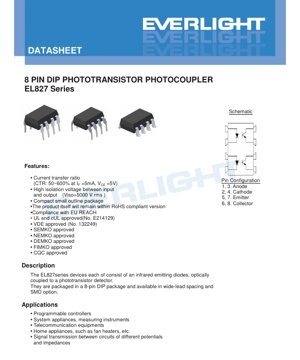
4.1 Pin Configuration and Schematic
The internal schematic shows the infrared emitting diode connected between pins 1/3 (anode) and 2/4 (cathode). The phototransistor's emitter is connected to pins 5/7, and its collector is connected to pins 6/8. Pins with identical functions are internally connected to provide mechanical strength and potentially reduce pin inductance. The standard connection is to use one pin from each pair.
Pin assignment:
- Pins 1, 3: Anode (A)
- Pin 2, 4: Cathode (K)
- Pin 5, 7: Emitter (E)
- Pin 6, 8: Collector (C)
4.2 Package Dimensions and Options
Detailed mechanical drawings are provided for each package variant:
- Standard DIP type:Traditional through-hole package.
- M option type:Features "wide pin bending", providing a pin pitch of 0.4 inches (approximately 10.16mm), which may be suitable for breadboards or specific layout requirements.
- S option type:Surface mount pin form for reflow soldering.
- S1 option type:A "low-profile" surface-mount lead form, which may have a lower standoff height compared to the S option.
The datasheet also includes recommended pad layouts for the surface-mount options (S and S1), which are crucial for achieving reliable solder joints and proper mechanical alignment during the reflow soldering process.
4.3 Device Marking
The device top is marked with "EL827" to indicate the series, followed by a one-digit year code (Y), a two-digit week code (WW), and an optional "V" suffix if the unit is VDE certified. This marking allows for tracing the production date and variant.
5. Soldering and Assembly Guide
5.1 Welding Conditions
The datasheet provides key information for the assembly process, especially for surface-mount variants. The maximum allowable body temperature during soldering is defined by the reflow profile referencing IPC/JEDEC J-STD-020D. Key parameters of this profile include:
- Preheating temperature:Minimum (Tsmin) 150°C, maximum (Tsmax) 200°C.
- Preheating time:The curve shows the specific time (ts) within this temperature range to gradually heat the component and the circuit board, minimizing thermal shock.
- Peak Temperature vs. Time:The curve must not exceed the maximum soldering temperature (TSOL) of 260°C, and the time above 260°C should be limited (typically as specified in the absolute maximum ratings, e.g., limited to 10 seconds).
Adhering to this curve is crucial to prevent damage to the plastic package, internal wire bonds, or the semiconductor die itself. For through-hole components, the 260°C, 10-second limit should also be observed during wave soldering or hand soldering.
6. Packaging and Ordering Information
6.1 Ordering Part Number Structure
Part number follows format: EL827X(Z)-V
- X:Lead form options: None (Standard DIP), M (Wide lead bend), S (Surface mount), S1 (Low-profile surface mount).
- Z:Reel packaging options: None (Tube), TA, or TB (different reel feed directions).
- V:Optional VDE safety certification mark.
6.2 Packaging Quantity
- Standard DIP and M options: 45 pieces per tube.
- S(TA), S(TB), S1(TA), S1(TB) options: 1000 pieces per reel.
6.3 Tape and Reel Specification
Detailed carrier tape dimensions are provided for the S and S1 options (TA and TB). Parameters include pocket dimensions (A, B, Do, D1), tape pitch (Po, P1), tape thickness (t), and overall tape width (W). Options TA and TB differ in the tape feed direction and must be correctly configured in the placement machine. The diagram shows the orientation of the device within the tape pocket.
7. Application Recommendations and Design Considerations
When designing with the EL827 optocoupler, several factors must be considered to ensure optimal performance and reliability.
Input circuit design:A current-limiting resistor must be connected in series with the input IRED. Its resistance is calculated based on the supply voltage (Vcc_in), the required forward current (IF), and the diode's voltage drop (VF): R_in = (Vcc_in - VF) / IF. The chosen IF affects CTR, switching speed, and device lifetime. It is recommended to operate at or below the recommended continuous operating current of 20mA.
Output circuit design:Phototransistors can be used in switching (saturation) mode or linear (amplification) mode. For digital switching, a pull-up resistor (RL) is connected between the collector and the output-side supply voltage (Vcc_out). The value of RL affects the switching speed (lower RL is faster, but higher IC) and current consumption. Ensure the output current (IC) does not exceed the maximum value of 50mA. For linear applications, the device operates in its active region, but the nonlinearity and temperature dependence of CTR must be carefully considered.
Isolation and Layout:To maintain a high isolation rating, ensure sufficient creepage distance and electrical clearance between the copper traces on the input and output sides of the PCB according to relevant safety standards (e.g., IEC 60950-1, IEC 62368-1). Place the optocoupler in the layout so that it straddles the isolation barrier.
Bypassing and Noise:For noise-sensitive applications or to improve the stability of switching circuits, consider placing a small bypass capacitor (e.g., 0.1 µF) near the power supply pins on the input and output sides of the device.
8. Technical Comparison and Frequently Asked Questions
8.1 Differences from Other Optocouplers
The main differences of EL827 are its high 5000Vrms isolation voltage and wide CTR range (50-600%). Compared to basic 4-pin optocouplers, the 8-pin DIP provides dual pins for each terminal, which can improve the mechanical fixation strength of the board and may offer slightly better thermal performance. The availability of surface-mount (S, S1) and wide-pin (M) options provides greater flexibility than many single-package products. Comprehensive international safety certifications (UL, VDE, etc.) are a significant advantage for commercial and industrial products requiring certification.
8.2 FAQ (Parameter-Based)
Q: What does a CTR range of 50-600% mean for my design?
A: This indicates production variation. You must design your circuit to reliably work with theminimumThe guaranteed CTR (50% in this case) works to ensure the output switches correctly under all conditions. If your design requires a specific sensitivity, you may need to select a device based on the measured CTR (binning) or use a circuit that can compensate for this variation.
Q: Can I use it for analog signal isolation?
A: While possible (using it in linear mode), it is not ideal due to the nonlinearity of CTR relative to IF and its strong temperature dependence. For precision analog isolation, dedicated linear optocouplers or isolation amplifiers are recommended.
Q: How do I choose between the S and S1 surface mount options?
A: Zaɓin S1 "Siriri" an tsara shi ne don aikace-aikacen da ke da ƙayyadaddun iyakar tsayi a cikin haɗin PCB. Dubi zanen girma na kunshe a cikin littafin bayanai, kwatanta tsayin daga allo da gabaɗayan girmansa. Halayen lantarki iri ɗaya ne.
Q: Lokacin sauyawa yana da alama yana jinkiri (har zuwa 18µs). Shin wannan ya dace da hanyar sadarwar dijital ta sauri ta ni?
A: Don daidaitaccen rarrabuwar dijital I/O a cikin hanyar haɗin PLC ko microcontroller, waɗannan saurin yawanci sun isa. Don saurin sadarwar jeri (misali, USB, RS-485 keɓance), ya kamata a yi la'akari da mai keɓance dijital mafi sauri (bisa capacitor ko haɗin maganadisu) ko kuma mai haɗin haske na sauri da aka tsara musamman don ƙimar bayanai a cikin kewayon Mbps.
9. Working Principles and Trends
9.1 Basic Working Principles
An optocoupler works by converting an electrical signal into light, transmitting that light across an electrically insulating gap, and then converting the light back into an electrical signal. In the EL827, current applied to the input infrared emitting diode (IRED) causes it to emit photons (light) at infrared wavelengths. This light passes through the transparent insulating molding compound and strikes the base region of the silicon phototransistor on the output side. The incident light generates electron-hole pairs in the base region, effectively acting as base current, thereby allowing a larger collector current to flow. This collector current is proportional to the incident light intensity, which in turn is proportional to the input diode current, establishing the Current Transfer Ratio (CTR). The key point is that the only connection between input and output is the light beam, thus providing electrical isolation.
9.2 Industry Trends
The optocoupler market continues to evolve. Key trends include the push for higher data rates to accommodate faster industrial communication protocols and digital power control. Demand for higher integration is also growing, such as integrating multiple isolated channels in a single package, or incorporating additional functions like IGBT/MOSFET gate drivers. Furthermore, the need for higher reliability, especially in automotive and industrial applications, is driving improvements in high-temperature performance and long-term CTR stability. While traditional phototransistor-based couplers like the EL827 remain a mainstay for basic isolation due to their simplicity, cost-effectiveness, and high-voltage capability, newer technologies like capacitive and magnetic (giant magnetoresistive) isolators are gaining increasing share in applications requiring extremely high speed, low power consumption, and robust noise immunity.
Detailed Explanation of LED Specification Terminology
Complete Explanation of LED Technical Terminology
I. Core Indicators of Photoelectric Performance
| Terminology | Unit/Representation | Popular Explanation | Why It Is Important |
|---|---|---|---|
| Luminous Efficacy | lm/W | The luminous flux emitted per watt of electrical power; higher values indicate greater energy efficiency. | Directly determines the energy efficiency rating and electricity cost of the lighting fixture. |
| Luminous Flux | lm (Lumen) | Total light output from a light source, commonly known as "brightness". | Determines if a luminaire is bright enough. |
| Viewing Angle | ° (degrees), e.g., 120° | The angle at which luminous intensity drops to half, determining the beam width. | Affects the illumination range and uniformity. |
| Color Temperature (CCT) | K (Kelvin), e.g., 2700K/6500K | The color temperature of light; lower values are yellowish/warm, higher values are whitish/cool. | Determines the lighting ambiance and suitable application scenarios. |
| Color Rendering Index (CRI / Ra) | Unitless, 0–100 | The ability of a light source to restore the true color of an object, Ra≥80 is recommended. | Affects color authenticity, used in high-demand places such as shopping malls and art galleries. |
| Color tolerance (SDCM) | MacAdam ellipse steps, e.g., "5-step" | A quantitative metric for color consistency; a smaller step number indicates better color consistency. | Ensure no color variation among luminaires from the same batch. |
| Dominant Wavelength | nm (nanometer), e.g., 620nm (red) | Thamani ya urefu wa wimbi inayolingana na rangi ya LED zenye rangi. | Inaamua hue ya LED moja-rangi kama nyekundu, manjano, kijani, n.k. |
| Spectral Distribution | Wavelength vs. Intensity Curve | Shows the intensity distribution of light emitted by an LED across various wavelengths. | Affects color rendering and color quality. |
II. Electrical Parameters
| Terminology | Symbol | Popular Explanation | Design Considerations |
|---|---|---|---|
| Forward Voltage | Vf | The minimum voltage required to light up an LED, similar to a "starting threshold". | The driving power supply voltage must be ≥ Vf, and the voltage accumulates when multiple LEDs are connected in series. |
| Forward Current | If | The current value that makes the LED emit light normally. | Constant current drive is often used, as current determines brightness and lifespan. |
| Maximum Pulse Current (Pulse Current) | Ifp | Peak current that can be withstood for a short period of time, used for dimming or flashing. | Pulse width and duty cycle must be strictly controlled to prevent overheating damage. |
| Reverse Voltage | Vr | The maximum reverse voltage that an LED can withstand; exceeding this may cause breakdown. | The circuit must be protected against reverse connection or voltage surges. |
| Thermal Resistance | Rth (°C/W) | The resistance to heat transfer from the chip to the solder joint; a lower value indicates better heat dissipation. | High thermal resistance requires a stronger heat dissipation design; otherwise, the junction temperature will increase. |
| Electrostatic Discharge Immunity (ESD Immunity) | V (HBM), e.g., 1000V | ESD strike resistance, higher value indicates less susceptibility to electrostatic damage. | Anti-static measures must be implemented during production, especially for high-sensitivity LEDs. |
III. Thermal Management and Reliability
| Terminology | Key Indicators | Popular Explanation | Impact |
|---|---|---|---|
| Junction Temperature | Tj (°C) | The actual operating temperature inside the LED chip. | For every 10°C reduction, the lifespan may double; excessively high temperatures cause lumen depreciation and color shift. |
| Lumen Depreciation | L70 / L80 (hours) | Time required for brightness to drop to 70% or 80% of its initial value. | Directly define the "useful life" of an LED. |
| Lumen Maintenance | % (e.g., 70%) | The percentage of remaining brightness after a period of use. | Characterization of luminance maintenance capability after long-term use. |
| Color Shift | Δu′v′ or MacAdam ellipse | The degree of color change during use. | Affects the color consistency of the lighting scene. |
| Thermal Aging | Material performance degradation | Deterioration of packaging materials due to prolonged high temperatures. | May lead to decreased brightness, color changes, or open-circuit failure. |
IV. Packaging and Materials
| Terminology | Common Types | Popular Explanation | Features and Applications |
|---|---|---|---|
| Package Types | EMC, PPA, Ceramic | A housing material that protects the chip and provides optical and thermal interfaces. | EMC has good heat resistance and low cost; ceramic has excellent heat dissipation and long lifespan. |
| Chip structure | Front side, Flip Chip | Chip electrode arrangement method. | Flip Chip offers better heat dissipation and higher luminous efficacy, suitable for high-power applications. |
| Phosphor coating | YAG, silicate, nitride | Coated on the blue LED chip, partially converted to yellow/red light, mixed to form white light. | Different phosphors affect luminous efficacy, color temperature, and color rendering. |
| Lens/Optical Design | Planar, microlens, total internal reflection | Optical structure on the encapsulation surface, controlling light distribution. | Determines the emission angle and light distribution curve. |
V. Quality Control and Binning
| Terminology | Binning Content | Popular Explanation | Purpose |
|---|---|---|---|
| Luminous Flux Binning | Codes such as 2G, 2H | Group by brightness level, each group has a minimum/maximum lumen value. | Ensure consistent brightness for products within the same batch. |
| Voltage binning | Codes such as 6W, 6X | Grouped by forward voltage range. | Facilitates driver power matching, improving system efficiency. |
| Color binning. | 5-step MacAdam ellipse | Group by color coordinates to ensure colors fall within an extremely small range. | Ensure color consistency to avoid color unevenness within the same luminaire. |
| Color temperature binning | 2700K, 3000K, etc. | Group by color temperature, each group has a corresponding coordinate range. | Meet the color temperature requirements of different scenarios. |
VI. Testing and Certification
| Terminology | Standard/Test | Popular Explanation | Significance |
|---|---|---|---|
| LM-80 | Lumen Maintenance Test | Long-term operation under constant temperature conditions, recording data on brightness attenuation. | Used to estimate LED lifespan (combined with TM-21). |
| TM-21 | Life Prediction Standard | Estimating lifespan under actual use conditions based on LM-80 data. | Providing scientific life prediction. |
| IESNA Standard | Illuminating Engineering Society Standard | Covering optical, electrical, and thermal testing methods. | Industry-recognized testing basis. |
| RoHS / REACH | Environmental Certification | Ensure products are free from hazardous substances (e.g., lead, mercury). | Conditions for market entry into the international market. |
| ENERGY STAR / DLC | Energy efficiency certification. | Energy Efficiency and Performance Certification for Lighting Products. | Commonly used in government procurement and subsidy programs to enhance market competitiveness. |