Table of Contents
- 1. Product Overview
- 1.1 Target Applications
- 2. In-depth Technical Parameter Analysis
- 2.1 Absolute Maximum Ratings
- 2.2 Electro-Optical Characteristics
- 2.2.1 Input (LED) Characteristics
- 2.2.2 Output (Phototransistor) Characteristics
- 2.2.3 Transfer Characteristics
- 3. Performance Curve Analysis
- 3.1 Relationship between Current Transfer Ratio (CTR) and Forward Current (IF)
- 3.2 Relationship between CTR and Temperature
- 3.3 Relationship between Collector Current and Collector-Emitter Voltage
- 4. Mechanical and Packaging Information
- 4.1 Pin Configuration
- 4.2 Package Dimensions and PCB Layout
- 5. Welding and Assembly Guide
- 6. Packaging and Ordering Information
- 6.1 Model Naming Rules
- 6.2 Packaging Options
- 6.3 Device Identification
- 7. Application Design Considerations
- 7.1 Driving the Input LED
- 7.2 Output Circuit Design
- 7.3 Using the Base Pin
- 7.4 Ensuring Reliable Isolation
- 8. Technical Comparison and Selection Guidance
- 9. Frequently Asked Questions (FAQ)
- 9.1 What are the differences between the EL20X and EL21X series?
- 9.2 How does temperature affect performance?
- 9.3 Shin wannan na'urar za a iya amfani da ita don keɓe siginar analog?
- What is the purpose of the "V" option in the 9.4 model?
- 10. Practical Design Examples
- 11. Working Principles
- 12. Technical Trends
1. Product Overview
EL20X ve EL21X serileri, fototransistör tabanlı optokuplör (optik kuplaj) ürün ailesidir ve standart 8-pinli Küçük Yüzey Montaj Paketi (SOP) kullanır. Bu cihazlar, kızılötesi ışık yayan diyot (LED) kullanarak sinyalleri bir fototransistör dedektörüne iletir ve böylece iki devre arasında elektriksel izolasyon sağlar. Ana işlevi, herhangi bir doğrudan elektriksel bağlantı olmadan, izolasyon bariyeri üzerinden elektrik sinyallerini iletmek ve böylece yüksek voltajın veya gürültünün bir devreden diğerine yayılmasını önlemektir.
The core advantage of this series lies in its combination of a compact, industry-standard SO-8 package size with robust isolation performance. Key features include a high isolation voltage of up to 3750 Vrms, a wide operating temperature range from -55°C to +110°C, and a high collector-emitter breakdown voltage (BVCEO). The device offers multiple Current Transfer Ratio (CTR) grades, enabling designers to select an optimized model based on the gain requirements of their specific application. Compliance with environmental and safety standards, such as halogen-free, lead-free, RoHS compliance, and UL/cUL certification, makes it suitable for a wide range of commercial and industrial applications.
1.1 Target Applications
These optocouplers are designed for general-purpose isolation and switching tasks in electronic systems. Typical application areas include:
- Feedback control circuits:Isolating feedback signals in switched-mode power supplies (SMPS) to maintain voltage regulation and protect the control IC.
- System Interface:Coupling digital or analog signals between circuits at different ground potentials or voltage levels, for example, in the interface between a microcontroller and a motor driver or industrial I/O modules.
- General-Purpose Switch:Replace mechanical relays to achieve noiseless solid-state signal switching.
- Monitoring and Detection Circuit:For applications where isolation is critical, such as safety monitoring, fault detection, or line detection.
2. In-depth Technical Parameter Analysis
This section provides a detailed and objective interpretation of the key electrical and optical parameters specified in the datasheet.
2.1 Absolute Maximum Ratings
These ratings define the stress limits that may cause permanent damage to the device. Operation under these conditions is not guaranteed.
- Input Forward Current (IF):60 mA (continuous). For very short pulses (10 µs), Peak Forward Current (IFM) is 1 A, which is related to the surge condition during the turn-on period.
- Input reverse voltage (VR):6 V. The reverse breakdown voltage of the input LED is relatively low; care must be taken in circuit design to avoid applying reverse bias.
- Output collector-emitter voltage (VCEO):80 V. This is the maximum voltage that can be withstood between the collector and emitter of the phototransistor when the base is open (no light input).
- Total power dissipation (PTOT):240 mW. This is the maximum total power that the input LED and output transistor can dissipate. The individual limits for input (PD) and output (PC) are 90 mW and 150 mW, respectively.
- Isolation voltage (VISO):3750 Vrms, for 1 minute. This is a critical safety parameter, tested by applying this AC voltage between all shorted input pins (1-4) and all shorted output pins (5-8). It verifies the dielectric strength of the internal insulation.
- Operating and Storage Temperature:-55°C to +110°C (operating), -55°C to +125°C (storage). The wide range ensures reliability in harsh environments.
2.2 Electro-Optical Characteristics
These parameters are measured under standard test conditions (unless specified, Ta=25°C), defining the performance of the device.
2.2.1 Input (LED) Characteristics
- Forward Voltage (VF):Typical value 1.3V, maximum 1.5V at IF= 10 mA. This is used to calculate the current-limiting resistor required for the LED drive circuit.
- Reverse current (IR):Maximum 100 µA at VR= 6V, indicating the leakage current of the LED in the off state.
2.2.2 Output (Phototransistor) Characteristics
- Collector-Emitter Dark Current (ICEO):Maximum 100 µA at VCE= 10V, IF= 0mA, maximum 50 nA. This is the leakage current of the phototransistor when there is no light irradiation, which is important for determining the signal level of the "off" state.
- Collector-emitter saturation voltage (VCE(sat)):In IF= 10mA, IC= 2mA, the maximum is 0.4V. When the device is used as a switch, the low saturation voltage helps minimize voltage drop and power loss.
2.2.3 Transfer Characteristics
The most critical parameter of an optocoupler is the Current Transfer Ratio (CTR).
- Definition:CTR = (IC/ IF) * 100%, where ICis the collector current of the phototransistor, IFis the forward current of the LED. It represents the efficiency of converting input current to output current.
- Grading System:This series is divided into specific CTR grades to ensure design consistency.
- EL20X series (standard CTR at IF=10mA):EL205 (40-80%), EL206 (63-125%), EL207 (100-200%), EL208 (160-320%).
- EL21X series (at IF=10mA minimum CTR):EL211(>20%)、EL212(>50%)、EL213(>100%)。
- Low current CTR (at IF=1mA):Different models (EL215, EL216, EL217) are specified for operation at lower LED currents, indicating that CTR depends on IF.
- Switching speed:Under specified test conditions (V=10V, I=2mA, R=100Ω), typical turn-on time (tonr) and turn-off time (tfoffCC) are each 3.0 µs, rise time (tC) is 1.6 µs, and the fall time (tL) is 2.2 µs. These parameters limit the maximum frequency of the signal that can be transmitted.
- Isolation parameters:Isolation resistance (RIO) Typical value is 1011Ω, input and output capacitance (CIO) typical value is 0.5 pF. Low capacitance is crucial for maintaining high common-mode transient immunity (CMTI) in noisy environments.
3. Performance Curve Analysis
Although the provided PDF excerpt mentions typical characteristic curves but does not show them, their general purpose and impact on design are explained as follows.
3.1 Current Transfer Ratio (CTR) vs. Forward Current (IF)
Typical curves show that CTR is not constant. It usually peaks at a specific IF(typically in the 1-10 mA range for such devices) and decreases at lower and higher currents. Designers must refer to this curve to select the optimal operating point that provides sufficient gain and linearity for their application.
3.2 Relationship between CTR and Temperature
CTR has a negative temperature coefficient; it decreases as the ambient temperature increases. This characteristic is crucial for designs operating across the full temperature range from -55°C to +110°C. The circuit design must ensure proper operation (e.g., sufficient output swing or switching capability) even at the maximum expected temperature, where CTR is at its minimum.
3.3 Relationship between Collector Current and Collector-Emitter Voltage
This set of curves with different IFB as parameters illustrates the output characteristics of the phototransistor. It demonstrates the saturation region (where VCEis low and ICC is primarily determined by IFControl) and the active/linear region. This is crucial for designing linear isolation amplifiers or ensuring the device is fully saturated when used as a switch.
4. Mechanical and Packaging Information
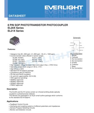
4.1 Pin Configuration
The pin arrangement of the 8-pin SOP package is as follows:Pin 1:Anode,Pin 2:Cathode,Pins 3, 4, 8:No Connection (NC),Pin 5:Emitter,Pin 6:Collector,Pin 7:Base. The base pin is brought out externally, which provides design flexibility. It can be left floating for maximum sensitivity, connected to the emitter through a resistor to reduce sensitivity and increase switching speed, or used for feedback in specific configurations.
4.2 Package Dimensions and PCB Layout
This device conforms to the standard SO-8 package dimensions. The datasheet contains detailed mechanical drawings with dimensions in millimeters. A recommended surface-mount assembly land pattern is also provided. Adhering to this land pattern is crucial for achieving reliable solder joints and preventing issues such as tombstoning during reflow soldering. The package outline ensures compatibility with automated pick-and-place equipment.
5. Welding and Assembly Guide
The absolute maximum rating for soldering temperature is 260°C for 10 seconds. This is a typical rating for lead-free reflow soldering processes. Standard guidelines from IPC/JEDEC J-STD-020 regarding Moisture Sensitivity Level (MSL) and reflow profiles should be followed. Devices should be stored in their original moisture barrier bag until use. If exposed to ambient humidity exceeding their MSL rating, baking is required prior to soldering to prevent "popcorn" damage during reflow.
6. Packaging and Ordering Information
6.1 Model Naming Rules
The model follows the format below:EL2XX(Y)-V
- XX:Model (05, 06, 07, 08, 11, 12, 13, 15, 16, 17). Define CTR rating.
- Y:Tape and reel packaging option (TA, TB, or blank indicates tube).
- V:Optional suffix, indicating inclusion of VDE safety certification.
6.2 Packaging Options
- Tube packaging:100 pieces per tube. Suitable for prototyping or small-batch manual assembly.
- Tape and reel packaging:2000 per reel. Designed for high-volume automatic assembly lines. The datasheet includes detailed reel specifications (cavity dimensions, tape width, reel diameter).
6.3 Device Identification
The top of the package is marked with "EL" (manufacturer code), part number (e.g., 207), a 1-digit year code (Y), and a 2-digit week code (WW). For VDE-certified versions, an optional "V" may be present. This marking allows for component traceability and verification.
7. Application Design Considerations
7.1 Driving the Input LED
An LED must be driven using a current-limiting resistor. The resistor value is calculated as RLIMIT= (VDRIVE- VF) / IF. Use the maximum V from the datasheetF, to ensure the required minimum I can be achieved under all conditions.F. For digital switches, considering the switching speed of the device, ensure the drive circuit can provide the necessary IF, to achieve the desired output state within the required time.
7.2 Output Circuit Design
The load resistor (RL) connected between the collector and VCC) determines the output voltage swing and switching speed. A smaller RLprovides faster switching speed (due to a smaller RC time constant), but results in a smaller output voltage swing and higher power consumption. A larger RLprovides a larger swing but slower speed. The selected IFand CTR must ensure that the phototransistor can sink sufficient current when turned on to pull the output voltage below the logic low threshold of the receiving circuit.
7.3 Using the Base Pin
Leaving the base pin (pin 7) open provides the highest CTR and sensitivity. Connecting a resistor (typically in the range of 100 kΩ to 1 MΩ) between the base and emitter (pin 5) shunts some of the photogenerated base current, reducing the effective gain (CTR) but significantly improving the switching speed, especially the turn-off time (toff). This is a common trade-off in high-speed digital isolation applications.
7.4 Ensuring Reliable Isolation
To maintain the rated isolation voltage, proper PCB layout is crucial. According to relevant safety standards (e.g., IEC 60950, IEC 60601), maintain sufficient creepage and clearance distances between the copper traces on the input and output sides on the PCB. The isolation barrier inside the component is certified, but the PCB layout must not compromise it.
8. Technical Comparison and Selection Guidance
The EL20X/EL21X series stands out with its isolation voltage of up to 3750V in the standard SO-8 package,rmswhich is higher than many basic 4-pin optocouplers. Compared to more advanced digital isolators (using CMOS technology), such phototransistor optocouplers are typically slower, have lower CTR, and CTR degrades over time. However, they offer excellent common-mode rejection, simplicity, and robustness for DC and low-frequency AC signal isolation. Key selection criteria are: required isolation voltage, necessary CTR at operating IF, acceptable switching speed, and operating temperature range.
9. Frequently Asked Questions (FAQ)
9.1 What are the differences between the EL20X and EL21X series?
The EL20X series (EL205-EL208) specifies both minimum and maximum CTR values (a "graded" range), providing tighter parameter control. The EL21X series (EL211-EL213) specifies only a minimum CTR value, which may result in a wider distribution of actual values but potentially at a lower cost.
9.2 How does temperature affect performance?
CTR decreases as temperature increases. For reliable operation across the entire temperature range, design calculations should use the minimum expected CTR at the maximum operating temperature. Datasheets typically provide derating curves or temperature coefficients for this purpose.
9.3 Shin wannan na'urar za a iya amfani da ita don keɓe siginar analog?
Yes, but with limitations. The response of the phototransistor is nonlinear, and the CTR varies with IFand temperature. For linear analog isolation, additional external circuitry (op-amp, feedback) is required to linearize the response, or dedicated linear optocouplers should be considered.
What is the purpose of the "V" option in the 9.4 model?
The "-V" suffix indicates that the specific unit has been tested and certified to comply with the VDE (Verband der Elektrotechnik, Elektronik und Informationstechnik) safety standard for reinforced insulation. This is typically a requirement for products sold in the European market.
10. Practical Design Examples
Scene:Isolate a 3.3V microcontroller GPIO pin to control a 12V relay coil on another circuit. The relay coil requires 50mA to energize.
Design Steps:
- Interface Selection:Using an optocoupler as a low-side switch for the relay. The microcontroller drives the LED side. The phototransistor will sink the relay coil current.
- Device Selection:Select a model with sufficient CTR. Required IC= 50mA. If the goal is to supply IF= 5mA from an MCU, then the required minimum CTR = (50mA / 5mA)*100% = 1000%. A standard phototransistor cannot provide this value. Therefore, the photocoupler must drive a small transistor ("post-transistor"), which then drives the relay. Select EL207 (CTR 100-200%) for good gain.
- Input circuit:MCU GPIO(3.3V)-> 限流电阻R1 -> EL207引脚1(阳极)和2(阴极)。R1 = (3.3V - 1.5V) / 0.005A = 360Ω(使用330Ω标准值)。
- Output circuit:12V电源 -> 继电器线圈 -> EL207的集电极(引脚6)。发射极(引脚5)接地。必须在继电器线圈两端反向并联一个续流二极管,以保护光敏三极管在关断时免受电压尖峰的影响。可以在引脚7添加一个基极-发射极电阻(例如1 MΩ)以改善关断速度。
- Verification:In IFAt =5mA, a minimum CTR of 100% can provide IC= 5mA. This is sufficient to saturate a small BJT with high gain (e.g., 2N3904), which can then switch a 50mA relay coil.
11. Working Principles
Photocoupler terdiri dari dua komponen utama yang dikemas dalam satu paket kedap cahaya. Di sisi input, sebuah dioda pemancar cahaya (LED) inframerah gallium arsenida (GaAs) mengubah arus listrik menjadi cahaya inframerah. Intensitas cahaya ini sebanding dengan arus maju (IF) yang mengalir melalui LED. Cahaya ini melintasi celah isolasi transparan (biasanya diisi dengan gel dielektrik) dan menyinari fototransistor silikon di sisi output. Daerah basis fototransistor dirancang sensitif terhadap panjang gelombang cahaya spesifik ini. Foton yang datang menghasilkan pasangan elektron-lubang di persimpangan basis-kolektor, membentuk arus foto yang berfungsi sebagai arus basis. Kemudian, arus basis fotogenerasi ini diperkuat oleh penguatan arus transistor (hFE), menghasilkan arus kolektor (I yang lebih besar.C). Ratio IC/IFis the Current Transfer Ratio (CTR). The key point is that the signal is transmitted via light, providing electrical isolation determined by the physical properties of the internal insulating material and the distance between the LED and the transistor.
12. Technical Trends
Photocouplers based on phototransistors, such as the EL20X/EL21X series, represent a mature and reliable isolation technology. The current trend in signal isolation includes the increasing adoption of digital isolators based on CMOS technology and those utilizing RF or capacitive coupling.Digital isolator。这些在速度(高达数百Mbps)、功耗、尺寸和寿命(无LED退化)方面具有显著优势。然而,传统光电耦合器在需要极高隔离电压(>5kV)、优异的共模瞬态抗扰度(CMTI)、简单性以及直流和低频隔离的成本效益的应用中仍保持强势地位。光电耦合器技术本身也在不断发展,例如将光敏三极管与基极-发射极电阻集成以提高速度(如基极引脚的可用性所示),以及开发具有更高爬电距离/电气间隙的封装以满足加强绝缘要求。
Detailed Explanation of LED Specification Terminology
Complete Interpretation of LED Technical Terminology
I. Core Indicators of Photoelectric Performance
| Terminology | Unit/Representation | Popular Explanation | Aiseā e Tāua ai |
|---|---|---|---|
| Luminous Efficacy | lm/W (lumens per watt) | The luminous flux emitted per watt of electrical power; higher values indicate greater energy efficiency. | It directly determines the energy efficiency rating of the luminaire and the electricity cost. |
| Luminous Flux | lm (lumen) | The total amount of light emitted by a light source, commonly known as "brightness". | Determines whether a luminaire is bright enough. |
| Viewing Angle | ° (degree), e.g., 120° | The angle at which luminous intensity drops to half, determining the beam width. | Affects the range and uniformity of illumination. |
| Color Temperature (CCT) | K (Kelvin), such as 2700K/6500K | Launin haske mai dumi ko sanyi, ƙananan ƙima sun karkata zuwa rawaya/dumi, manyan ƙima sun karkata zuwa fari/sanyi. | Yana ƙayyade yanayin hasken wuta da yanayin da ya dace. |
| Color Rendering Index (CRI / Ra) | Unitless, 0–100 | The ability of a light source to reproduce the true colors of objects, with Ra≥80 being preferable. | Affects color fidelity, used in high-demand places such as shopping malls and art galleries. |
| Color tolerance (SDCM) | MacAdam ellipse step, such as "5-step" | A quantitative indicator of color consistency; the smaller the step number, the better the color consistency. | Ensure no color difference among luminaires from the same batch. |
| Dominant Wavelength | nm (nanometer), e.g., 620nm (red) | Wavelength values corresponding to the colors of colored LEDs. | Determines the hue of monochromatic LEDs such as red, yellow, and green. |
| Spectral Distribution | Wavelength vs. Intensity Curve | Shows the intensity distribution of light emitted by an LED at each wavelength. | Affects color rendering and color quality. |
II. Electrical Parameters
| Terminology | Symbol | Popular Explanation | Design Considerations |
|---|---|---|---|
| Forward Voltage | Vf | The minimum voltage required to light up an LED, similar to a "starting threshold". | The driving power supply voltage must be ≥ Vf; the voltages add up when multiple LEDs are connected in series. |
| Forward Current | If | The current value that makes the LED emit light normally. | Constant current drive is often used, as current determines brightness and lifespan. |
| Maximum Pulse Current | Ifp | The peak current that can be withstood for a short period of time, used for dimming or flashing. | Pulse width and duty cycle must be strictly controlled to prevent overheating damage. |
| Reverse Voltage | Vr | Maximum reverse voltage that an LED can withstand; exceeding it may cause breakdown. | Reverse connection or voltage surges must be prevented in the circuit. |
| Thermal Resistance (Thermal Resistance) | Rth (°C/W) | The resistance to heat flow from the chip to the solder joint. A lower value indicates better heat dissipation. | High thermal resistance requires stronger heat dissipation design, otherwise junction temperature rises. |
| Electrostatic Discharge Immunity (ESD Immunity) | V (HBM), such as 1000V | Electrostatic discharge immunity; a higher value indicates greater resistance to damage from static electricity. | Anti-static measures must be implemented during production, especially for high-sensitivity LEDs. |
III. Thermal Management and Reliability
| Terminology | Key Indicators | Popular Explanation | Impact |
|---|---|---|---|
| Junction Temperature | Tj (°C) | The actual operating temperature inside the LED chip. | For every 10°C reduction, the lifespan may double; excessively high temperatures cause lumen depreciation and color shift. |
| Lumen Depreciation | L70 / L80 (hours) | The time required for the brightness to drop to 70% or 80% of its initial value. | Directly define the "useful life" of an LED. |
| Lumen Maintenance | % (e.g., 70%) | The percentage of remaining brightness after a period of use. | Characterizes the ability to maintain brightness after long-term use. |
| Color Shift | Δu′v′ or MacAdam ellipse | The degree of color change during use. | Affects the color consistency of the lighting scene. |
| Thermal Aging | Material performance degradation | Degradation of packaging materials due to prolonged high temperatures. | It may lead to a decrease in brightness, color change, or open-circuit failure. |
IV. Packaging and Materials
| Terminology | Common Types | Popular Explanation | Characteristics and Applications |
|---|---|---|---|
| Package Types | EMC, PPA, Ceramic | The housing material that protects the chip and provides optical and thermal interfaces. | EMC offers good heat resistance and low cost; ceramic provides superior heat dissipation and long lifespan. |
| Chip Structure | Front-side, Flip Chip | Chip electrode arrangement method. | Flip-chip offers better heat dissipation and higher luminous efficacy, suitable for high-power applications. |
| Phosphor coating. | YAG, silicate, nitride | Coated on the blue LED chip, partially converted to yellow/red light, mixed to form white light. | Different phosphors affect luminous efficacy, color temperature, and color rendering. |
| Lens/Optical Design | Flat, microlens, total internal reflection | Optical structure on the packaging surface, controlling light distribution. | Determines the emission angle and light distribution curve. |
V. Quality Control and Grading
| Terminology | Grading Content | Popular Explanation | Purpose |
|---|---|---|---|
| Luminous Flux Binning | Codes such as 2G, 2H | Group by brightness level, each group has a minimum/maximum lumen value. | Ensure consistent brightness for products in the same batch. |
| Voltage binning | Code such as 6W, 6X | Grouped by forward voltage range. | Ease of matching the driving power supply, improving system efficiency. |
| Color binning | 5-step MacAdam ellipse | Group by color coordinates to ensure colors fall within a minimal range. | Ensure color consistency to avoid uneven colors within the same luminaire. |
| Color Temperature Grading | 2700K, 3000K, etc. | Group by color temperature, each group has a corresponding coordinate range. | Meet the color temperature requirements of different scenarios. |
VI. Testing and Certification
| Terminology | Standard/Test | Popular Explanation | Meaning |
|---|---|---|---|
| LM-80 | Lumen Maintenance Test | Long-term operation under constant temperature conditions, recording luminance attenuation data. | For estimating LED lifetime (in conjunction with TM-21). |
| TM-21 | Lifetime projection standard | Estimating lifespan under actual usage conditions based on LM-80 data. | Providing scientific life prediction. |
| IESNA Standard | Illuminating Engineering Society Standard | Covers optical, electrical, and thermal testing methods. | Industry-recognized testing basis. |
| RoHS / REACH | Environmental Certification | Ensure the product does not contain harmful substances (e.g., lead, mercury). | Entry requirements for the international market. |
| ENERGY STAR / DLC | Energy efficiency certification | Energy efficiency and performance certification for lighting products. | Commonly used in government procurement and subsidy programs to enhance market competitiveness. |