Teburin Abubuwan Ciki
- 1. Bayanin Samfur
- 2. Fassarar Ma'ana Mai Zurfi na Sigogi na Fasaha
- 2.1 Halayen Hasken Haske da Na Lantarki
- 2.2 Matsakaicin Matsakaici na Ƙarshe da Halayen Zafi
- 3. Bayanin Tsarin Rarrabuwa
- 3.1 Rarrabuwar Ƙarfin Haske
- 3.2 Rarrabuwar Ƙarfin Lantarki na Gaba
- 3.3 Rarrabuwar Launi (Chromaticity)
- 4. Bincike na Lanƙwasa Aiki
- 4.1 Ƙarfin Lantarki na Gaba da Ƙarfin Lantarki na Gaba (Lanƙwasa IV)
- 4.2 Dangantakar Ƙarfin Haske da Ƙarfin Lantarki na Gaba
- 4.3 Jadawalin Aikin Zafi
- 4.4 Lanƙwasa Rage Ƙarfin Lantarki na Gaba
- 4.5 Rarraba Bakan Haske
- 5. Bayanan Injiniya da Kunshi
- 6. Jagororin Solder da Haɗawa
- 6.1 Tsarin Solder Pad da Aka Ba da Shawara
- 6.2 Bayanin Yanayin Solder Reflow
- 6.3 Abubuwan Kariya don Amfani
- 7. Bayanan Kunshi da Oda
- 8. Shawarwari na Aikace-aikace
- 8.1 Yanayin Aikace-aikace na Al'ada
- 8.2 Abubuwan Ƙirar Ƙira
- 9. Kwatancen Fasaha da Bambance-bambance
- 10. Tambayoyin da Ake Yawan Yi (Dangane da Sigogi na Fasaha)
- 11. Ƙirar Aiki da Amfani na Aiki
- 12. Gabatarwar Ka'ida
- 13. Trends na Ci Gaba
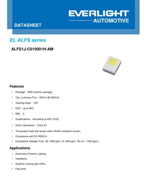
1. Bayanin Samfur
ALFS1J-C0 babban LED ne mai ƙarfi, mai hawa a saman, wanda aka ƙera musamman don aikace-aikacen hasken waje na mota masu buƙatu. An saka shi a cikin kunshin yumbu mai ƙarfi, yana ba da ingantaccen sarrafa zafi da amincin a ƙarƙashin yanayi mai tsanani. Na'urar tana da cancanta bisa ga ƙa'idodin AEC-Q102, yana tabbatar da cewa ta cika ƙa'idodi masu tsauri don kayan lantarki na mota. Aikace-aikacensa na farko sun haɗa da fitilun mota, fitilun gudu na rana (DRL), da fitilun hazo, inda aikin daidaitawa, babban fitarwa na haske, da dorewa na dogon lokaci suke da mahimmanci.
Babban fa'idodin wannan LED sun haɗa da babban ƙarfin haske na al'ada na lumens 425 a lokacin tuƙi na 1000mA, faɗin kwanar kallo na digiri 120 don kyakkyawan rarraba haske, da ƙirar ƙarfi tare da kariya ta ESD har zuwa 8 kV (HBM). Hakanan yana bin ka'idojin RoHS, REACH, da ƙa'idodin marasa halogen, yana sa ya dace da kasuwannin motoci na duniya. Ƙarfin sulfur na samfurin an rarraba shi azaman A1, yana nuna babban juriya ga yanayin iska mai ɗauke da sulfur da ake samu a yanayin mota.
2. Fassarar Ma'ana Mai Zurfi na Sigogi na Fasaha
2.1 Halayen Hasken Haske da Na Lantarki
An ayyana mahimman sigogi na aiki a ƙarƙashin yanayin gwaji na ƙarfin lantarki na gaba (IF) na 1000mA tare da kiyaye farantin zafi a 25°C. Ƙarfin haske na al'ada (Φv) shine 425 lm, tare da mafi ƙarancin 400 lm da matsakaicin 500 lm, ƙarƙashin ƙimar auna na ±8%. Ƙarfin lantarki na gaba (VF) yawanci yana auna 3.25V, daga 2.90V zuwa 3.80V (±0.05V tolerance). Tsawon zango ko daidaitaccen zafin launi (CCT) yana cikin kewayon 5391K zuwa 6893K, yana rarraba shi azaman LED farin sanyi. An ƙayyade kwanar kallo a matsayin digiri 120, tare da jurewar ±5°.
2.2 Matsakaicin Matsakaici na Ƙarshe da Halayen Zafi
These ratings define the limits beyond which permanent damage may occur. The absolute maximum forward current is 1500 mA. The device is not designed for reverse voltage operation. The maximum junction temperature (TJ) is 150°C, with an operating temperature range of -40°C to +125°C. The thermal resistance from the junction to the solder point is a critical parameter for heat dissipation. The real thermal resistance (Rth JS real) is typ. 4.0 K/W (max 4.4 K/W), while the electrical equivalent (Rth JS el) is typ. 3.0 K/W (max 3.4 K/W). The maximum power dissipation is 5700 mW.
. Binning System Explanation
To ensure color and brightness consistency in production, LEDs are sorted into bins based on key parameters.
.1 Luminous Flux Binning
Luminous flux is binned in groups, with the provided data showing Group "C". Within this group, bins are defined: Bin 6 (400-425 lm), Bin 7 (425-450 lm), Bin 8 (450-475 lm), and Bin 9 (475-500 lm). The test is performed at the typical forward current with a 25ms pulse, and measurement tolerance is ±8%.
.2 Forward Voltage Binning
Forward voltage is categorized into three groups: Group 1A (2.90V - 3.20V), Group 1B (3.20V - 3.50V), and Group 1C (3.50V - 3.80V). This allows designers to select LEDs with similar VFfor better current matching in multi-LED arrays. The measurement tolerance is ±0.05V.
.3 Color (Chromaticity) Binning
The color coordinates on the CIE 1931 chromaticity diagram are binned into specific regions. The datasheet shows bins for cool white LEDs, including 63M, 61M, 58M, 56M, 65L, 65H, 61L, and 61H. Each bin is defined by a quadrilateral area on the x,y coordinate plot. For example, Bin 63M covers coordinates approximately from (0.3127, 0.3093) to (0.3212, 0.3175). The coordinate measurement tolerance is ±0.005.
. Performance Curve Analysis
.1 Forward Current vs. Forward Voltage (IV Curve)
The graph shows the non-linear relationship between forward current and forward voltage at 25°C. The curve is typical for a power LED, with voltage increasing logarithmically with current. This data is essential for designing the driver circuit to ensure the LED operates within its specified voltage range at the desired current.
.2 Relative Luminous Flux vs. Forward Current
This graph illustrates light output relative to the value at 1000mA as a function of drive current. Luminous flux increases with current but may exhibit sub-linear growth at higher currents due to efficiency droop and increased junction temperature.
.3 Thermal Performance Graphs
Several graphs depict performance versus junction temperature (TJ) at IF=1000mA. TheRelative Luminous Flux vs. Junction Temperaturecurve shows the light output decreasing as temperature rises, a characteristic known as thermal quenching. TheRelative Forward Voltage vs. Junction Temperaturecurve shows VFdecreasing linearly with increasing temperature, which can be used for junction temperature estimation. TheChromaticity Coordinates Shift vs. Junction Temperaturegraph shows how the color point (CIE x, y) changes with temperature, which is crucial for color-critical applications.
.4 Forward Current Derating Curve
This is a critical design graph. It plots the maximum allowable forward current against the solder pad temperature (TS). As TSincreases, the maximum permissible current must be reduced to prevent the junction temperature from exceeding 150°C. The curve provides specific derating points: e.g., at TS=110°C, IFcan be 1500mA; at TS=125°C, IFmust be reduced to 1200mA. Operation below 50mA is not recommended.
.5 Spectral Distribution
The relative spectral power distribution graph shows the intensity of light emitted across wavelengths from approximately 400nm to 800nm at 25°C and 1000mA. It characterizes the LED's cool white light, typically produced by a blue LED chip combined with a phosphor layer.
. Mechanical and Package Information
The LED uses a surface-mount device (SMD) ceramic package. Ceramic offers superior thermal conductivity compared to plastic packages, facilitating better heat transfer from the LED junction to the printed circuit board (PCB). This is vital for maintaining performance and longevity in high-power applications like automotive lighting. The specific mechanical dimensions, including length, width, height, and pad locations, are detailed in the mechanical drawing section of the datasheet. The package includes a thermal pad for efficient soldering to a thermal land on the PCB.
. Soldering and Assembly Guidelines
.1 Recommended Soldering Pad Layout
A recommended land pattern (footprint) for PCB design is provided. This pattern ensures proper solder joint formation, electrical connection, and most importantly, optimal thermal transfer from the LED's thermal pad to the PCB's copper plane. Adhering to this layout is crucial for reliability.
.2 Reflow Soldering Profile
The datasheet specifies a reflow soldering profile with a peak temperature of 260°C. This profile defines the time-temperature curve that the assembly must follow during the reflow process. Key parameters include preheat, soak, reflow, and cooling rates and durations. Following this profile prevents thermal shock to the ceramic package and ensures reliable solder joints without damaging the internal LED structure.
.3 Precautions for Use
General handling and usage precautions are outlined. These include warnings against applying reverse voltage, exceeding absolute maximum ratings, and improper soldering techniques. It also emphasizes the importance of static discharge (ESD) protection during handling, even though the device has built-in ESD protection up to 8kV.
. Packaging and Ordering Information
The product is supplied in tape and reel packaging suitable for automated pick-and-place assembly machines. Packaging information details the reel dimensions, tape width, pocket spacing, and orientation of the components on the tape. The part number structure (e.g., ALFS1J-C010001H-AM) encodes specific attributes such as the series, bin codes for flux and color, and other variant information. Ordering information guides the user on how to specify the desired bin combinations when placing an order.
. Application Suggestions
.1 Typical Application Scenarios
The primary designed applications areAutomotive Exterior Lightingsystems. This includes:
- Headlamps (Low/High Beam): Where high luminous intensity and precise beam control are required.
- Daytime Running Lights (DRL): Requiring high efficiency and visibility.
- Fog Lamps: Needing good penetration in adverse weather conditions.
The wide viewing angle and high flux make it suitable for both primary light sources and supplementary lighting functions.
.2 Design Considerations
1. Thermal Management: This is the most critical aspect. The PCB must have an adequate thermal design—using thick copper layers, thermal vias, and possibly an external heatsink—to keep the solder pad temperature (TS) as low as possible. Refer to the derating curve for current limits.
2. Drive Current: While the LED can be driven up to 1500mA, operating at or below the typical 1000mA provides a better balance of light output, efficiency, and thermal load, enhancing long-term reliability.
3. Optical Design: The 120° viewing angle requires appropriate secondary optics (lenses, reflectors) to shape the beam for the specific application (e.g., a focused beam for headlights).
4. Electrical Design: Use a constant-current LED driver compatible with the forward voltage bin. For arrays, consider bin selection and possible use of current-balancing techniques.
. Technical Comparison and Differentiation
Compared to standard commercial or industrial LEDs, the ALFS1J-C0 offers several key differentiators essential for automotive use:
- AEC-Q102 Qualification: This is a mandatory reliability standard for automotive LEDs, involving rigorous tests for temperature cycling, humidity, solder heat resistance, and more.
- Ceramic Package: Provides better thermal performance and long-term stability under high temperature and humidity than plastic packages (e.g., PPA, PCT).
- Sulfur Robustness (Class A1): Specifically tested and guaranteed to resist corrosion from sulfur-containing gases, a common failure mode in automotive environments.
- High ESD Rating (8kV HBM): Offers greater protection against electrostatic discharge during handling and assembly.
- Extended Temperature Range (-40°C to +125°C): Guarantees operation in the extreme temperatures encountered by vehicles.
. Frequently Asked Questions (Based on Technical Parameters)
Q: What is the actual light output I can expect from Bin C7?
A: Bin C7 specifies a luminous flux range of 425-450 lm when measured at IF=1000mA and Ts=25°C. Considering the ±8% measurement tolerance, the actual measured value for a specific LED could be between approximately 391 lm and 486 lm under those ideal test conditions. In a real application with higher temperature, the output will be lower.
Q: How do I determine the required heatsink based on the thermal data?
A: You need to perform a thermal calculation. The key parameter is the real thermal resistance, Rth JS real(typ. 4.0 K/W). This is the resistance from the junction to the solder point. You must add the thermal resistance from the solder point to the ambient (through the PCB, thermal interface material, and heatsink) to calculate the total Rth JA. Using the formula TJ= TA+ (Rth JA× Power Dissipation), you can ensure TJremains below 150°C, preferably with a safety margin. The derating curve provides a simplified guide based on solder pad temperature.
Q: Can I drive this LED with a constant voltage source?
A: It is strongly discouraged. LEDs are current-driven devices. Their forward voltage has a negative temperature coefficient and varies from unit to unit (as seen in the voltage bins). A constant voltage source could lead to thermal runaway: as the LED heats up, VFdrops, causing current to increase, which generates more heat, further dropping VFand increasing current until failure. Always use a constant-current driver or a circuit that actively regulates the current.
. Practical Design and Usage Case
Case: Designing a Daytime Running Light (DRL) Module
A designer is creating a DRL module for a passenger car. The design calls for 6 LEDs to achieve the desired brightness and form factor.
1. Bin Selection: To ensure uniform appearance, the designer specifies tight color bins (e.g., 61M ± 1 step) and a single luminous flux bin (e.g., C7). They may also specify a tight forward voltage bin (e.g., 1A) to improve current sharing in a simple series configuration.
2. Thermal Design: The module will be mounted in a confined space. The designer uses a metal-core PCB (MCPCB) with a 2oz copper layer. Thermal simulation is run to ensure the solder pad temperature does not exceed 110°C in the worst-case ambient temperature (e.g., 85°C inside the headlamp assembly). According to the derating curve, at TS=110°C, the full 1500mA is permissible, but the designer chooses to drive at 1000mA for better efficacy and longevity.
3. Electrical Design: The 6 LEDs are placed in a series string. The total forward voltage at 1000mA will be approximately 6 × 3.25V = 19.5V (typ), but could range from ~17.4V to 22.8V based on binning. A buck-boost constant-current LED driver is selected to accommodate this voltage range from a 12V automotive battery system (nominal 12V, but operating from 9V to 16V).
4. Optical Design: A secondary optic (a TIR lens) is designed over each LED to collimate the 120° emission into a controlled horizontal fan beam suitable for a DRL signature.
. Principle Introduction
The ALFS1J-C0 is a phosphor-converted white LED. The fundamental principle involves a semiconductor chip (typically made of indium gallium nitride - InGaN) that emits blue light when forward biased (electroluminescence). This blue light is partially absorbed by a cerium-doped yttrium aluminum garnet (YAG:Ce) phosphor layer deposited over the chip. The phosphor down-converts a portion of the blue photons to longer wavelengths, primarily in the yellow region. The mixture of the remaining blue light and the converted yellow light is perceived by the human eye as white light. The exact ratio of blue to yellow, and the inclusion of other phosphors, determines the correlated color temperature (CCT) and color rendering index (CRI). The ceramic package serves as a robust substrate for mounting the chip and phosphor, and as an efficient heat spreader.
. Development Trends
The evolution of automotive LEDs like the ALFS1J-C0 follows several clear industry trends:
1. Increased Luminous Efficacy (lm/W): Ongoing improvements in chip design, phosphor efficiency, and package thermal management aim to deliver more light output for the same electrical input power, reducing energy consumption and thermal load.
2. Higher Power Density and Miniaturization: There is a push to achieve higher flux from smaller package footprints, enabling more compact and stylized lighting designs.
3. Improved Color Consistency and Stability: Advancements in phosphor technology and binning processes lead to tighter color tolerances and reduced color shift over temperature and lifetime.
4. Enhanced Reliability and Robustness: Standards like AEC-Q102 are continuously evolving, and new tests are added to address real-world failure modes, such as sulfur resistance, which has become a key requirement.
5. Integration and Smart Lighting: The future points towards integrated modules that combine LEDs, drivers, sensors, and communication interfaces for adaptive front-lighting systems (AFS) and communication via light (Li-Fi or V2X signaling).
6. Specialized Spectra: Development of spectra optimized for specific purposes, such as improved visibility in fog or reduced glare for oncoming traffic, is an active area of research.
Kalmomin Ƙayyadaddun LED
Cikakken bayanin kalmomin fasaha na LED
Aikin Hasken Wutar Lantarki
| Kalma | Naúrar/Wakilci | Bayanin Sauri | Me yasa yake da muhimmanci |
|---|---|---|---|
| Ingancin Hasken Wuta | lm/W (lumen kowace watt) | Fitowar haske kowace watt na wutar lantarki, mafi girma yana nufin mafi ingancin kuzari. | Kai tsaye yana ƙayyade matakin ingancin kuzari da farashin wutar lantarki. |
| Gudun Hasken Wuta | lm (lumen) | Jimillar hasken da tushe ke fitarwa, ana kiransa "haske". | Yana ƙayyade ko hasken yana da haske sosai. |
| Kusurwar Dubawa | ° (digiri), misali 120° | Kusurwar da ƙarfin haske ya ragu zuwa rabi, yana ƙayyade faɗin haske. | Yana shafar kewar haskakawa da daidaito. |
| Zafin Launi (CCT) | K (Kelvin), misali 2700K/6500K | Zafi/sanyin haske, ƙananan ƙimomi rawaya/zafi, mafi girma fari/sanyi. | Yana ƙayyade yanayin haskakawa da yanayin da suka dace. |
| CI / Ra | Ba naúrar, 0–100 | Ikon ba da launukan abubuwa daidai, Ra≥80 yana da kyau. | Yana shafar sahihancin launi, ana amfani dashi a wurare masu buƙatu kamar shaguna, gidajen tarihi. |
| SDCM | Matakan ellipse MacAdam, misali "5-mataki" | Ma'aunin daidaiton launi, ƙananan matakai suna nufin mafi daidaiton launi. | Yana tabbatar da daidaiton launi a cikin rukunin LED iri ɗaya. |
| Matsakaicin Tsawon Raɗaɗin Hasken | nm (nanomita), misali 620nm (ja) | Tsawon raɗaɗin haske daidai da launin LED masu launi. | Yana ƙayyade launin ja, rawaya, kore LED masu launi ɗaya. |
| Rarraba Bakan Hasken | Layin tsawon raɗaɗi da ƙarfi | Yana nuna rarraba ƙarfi a cikin tsawon raɗaɗin haske. | Yana shafar ba da launi da ingancin launi. |
Ma'auni na Lantarki
| Kalma | Alamar | Bayanin Sauri | Abubuwan ƙira |
|---|---|---|---|
| Ƙarfin lantarki na gaba | Vf | Mafi ƙarancin ƙarfin lantarki don kunna LED, kamar "maƙallan farawa". | Ƙarfin lantarki na injin dole ya zama ≥Vf, ƙarfin lantarki yana ƙara don LED a jere. |
| Ƙarfin lantarki na gaba | If | Ƙimar ƙarfin lantarki don aikin LED na yau da kullun. | Yawanci tuƙi mai ƙarfi akai-akai, ƙarfin lantarki yana ƙayyade haske da tsawon rai. |
| Matsakaicin Ƙarfin lantarki na bugun jini | Ifp | Matsakaicin ƙarfin lantarki mai jurewa na ɗan lokaci, ana amfani dashi don duhu ko walƙiya. | Fadin bugun jini da sake zagayowar aiki dole ne a sarrafa su sosai don guje wa lalacewa. |
| Ƙarfin lantarki na baya | Vr | Matsakaicin ƙarfin lantarki na baya da LED zai iya jurewa, wanda ya wuce zai iya haifar da rushewa. | Dangane dole ne ya hana haɗin baya ko ƙarfin lantarki. |
| Juriya na zafi | Rth (°C/W) | Juriya ga canja wurin zafi daga guntu zuwa solder, ƙasa yana da kyau. | Babban juriya na zafi yana buƙatar zubar da zafi mai ƙarfi. |
| Rigakafin ESD | V (HBM), misali 1000V | Ikon jurewa zubar da wutar lantarki, mafi girma yana nufin ƙasa mai rauni. | Ana buƙatar matakan hana wutar lantarki a cikin samarwa, musamman ga LED masu hankali. |
Gudanar da Zafi & Amincewa
| Kalma | Ma'aunin maɓalli | Bayanin Sauri | Tasiri |
|---|---|---|---|
| Zazzabin Haɗin gwiwa | Tj (°C) | Ainihin yanayin aiki a cikin guntun LED. | Kowane raguwa 10°C na iya ninka tsawon rai; yayi yawa yana haifar da lalacewar haske, canjin launi. |
| Ragewar Lumen | L70 / L80 (sa'o'i) | Lokacin da haske ya ragu zuwa 70% ko 80% na farko. | Kai tsaye yana ayyana "tsawon sabis" na LED. |
| Kula da Lumen | % (misali 70%) | Kashi na hasken da aka riƙe bayan lokaci. | Yana nuna riƙon haske akan amfani na dogon lokaci. |
| Canjin Launi | Δu′v′ ko ellipse MacAdam | Matsakaicin canjin launi yayin amfani. | Yana shafar daidaiton launi a cikin yanayin haskakawa. |
| Tsufa na Zafi | Lalacewar kayan aiki | Lalacewa saboda yanayin zafi na dogon lokaci. | Zai iya haifar da raguwar haske, canjin launi, ko gazawar buɗe kewaye. |
Tufafi & Kayan Aiki
| Kalma | Nau'ikan gama gari | Bayanin Sauri | Siffofi & Aikace-aikace |
|---|---|---|---|
| Nau'in Kunshin | EMC, PPA, Yumbu | Kayan gida masu kare guntu, samar da hanyar sadarwa ta gani/zafi. | EMC: juriya mai kyau na zafi, farashi mai rahusa; Yumbu: mafi kyawun zubar da zafi, tsawon rai. |
| Tsarin Guntu | Gaba, Guntu Juyawa | Tsarin na'urorin lantarki na guntu. | Juyawar guntu: mafi kyawun zubar da zafi, inganci mafi girma, don ƙarfi mai ƙarfi. |
| Rufin Phosphor | YAG, Silicate, Nitride | Yana rufe guntu shuɗi, yana canza wasu zuwa rawaya/ja, yana haɗa su zuwa fari. | Phosphor daban-daban suna shafar inganci, CCT, da CRI. |
| Ruwan tabarau/Optics | Lefi, Microlens, TIR | Tsarin gani a saman yana sarrafa rarraba haske. | Yana ƙayyade kusurwar dubawa da layin rarraba haske. |
Kula da Inganci & Rarraba
| Kalma | Abun rarraba | Bayanin Sauri | Manufa |
|---|---|---|---|
| Kwalin Gudun Hasken | Lambar misali 2G, 2H | An tattara su ta hanyar haske, kowace ƙungiya tana da ƙananan/matsakaicin ƙimar lumen. | Yana tabbatar da daidaiton haske a cikin jeri ɗaya. |
| Kwalin Ƙarfin lantarki | Lambar misali 6W, 6X | An tattara su ta hanyar kewayon ƙarfin lantarki na gaba. | Yana sauƙaƙe daidaitawar tuƙi, yana inganta ingancin tsarin. |
| Kwalin Launi | Ellipse MacAdam 5-mataki | An tattara su ta hanyar daidaitattun launi, yana tabbatar da ƙuntataccen kewayon. | Yana ba da garantin daidaiton launi, yana guje wa launi mara daidaituwa a cikin kayan aikin. |
| Kwalin CCT | 2700K, 3000K da sauransu | An tattara su ta hanyar CCT, kowanne yana da madaidaicin kewayon daidaitawa. | Yana cika buƙatun CCT na yanayi daban-daban. |
Gwaji & Takaddun Shaida
| Kalma | Matsakaicin/Gwaji | Bayanin Sauri | Muhimmanci |
|---|---|---|---|
| LM-80 | Gwajin kula da lumen | Haskakawa na dogon lokaci a yanayin zafi akai-akai, yana rikodin lalacewar haske. | Ana amfani dashi don kimanta rayuwar LED (tare da TM-21). |
| TM-21 | Matsakaicin kimanta rayuwa | Yana kimanta rayuwa a ƙarƙashin yanayi na ainihi bisa bayanan LM-80. | Yana ba da hasashen kimiyya na rayuwa. |
| IESNA | Ƙungiyar Injiniyoyin Haskakawa | Yana rufe hanyoyin gwajin gani, lantarki, zafi. | Tushen gwaji da masana'antu suka amince. |
| RoHS / REACH | Tabbatarwar muhalli | Yana tabbatar da babu abubuwa masu cutarwa (darma, mercury). | Bukatar shiga kasuwa a duniya. |
| ENERGY STAR / DLC | Tabbatarwar ingancin kuzari | Tabbatarwar ingancin kuzari da aiki don samfuran haskakawa. | Ana amfani dashi a cikin sayayyan gwamnati, shirye-shiryen tallafi, yana haɓaka gasa. |