Table of Contents
- 1. Product Overview
- 1.1 Core Advantages and Target Market
- 2. In-depth Technical Parameter Analysis
- 2.1 Absolute Maximum Ratings
- 2.2 Electro-Optical Characteristics
- 4.1 Relative Intensity vs. Wavelength
- 4.2 Directivity Pattern
- 4.3 Forward Current vs. Forward Voltage (I-V Curve)
- 4.4 Relative Intensity vs. Forward Current (L-I Curve)
- 4.5 Thermal Characteristics
- 5.1 Package Dimensions and Drawings
- 5.2 Polarity Identification
- 6.1 Lead Forming
- 6.2 Storage Conditions
- 6.3 Welding Process
- 6.4 Cleaning
- 6.5 Thermal Management
- 6.6 Electrostatic Discharge (ESD) Protection
- 7.1 Packaging Specifications
- 7.2 Labeling Instructions
- 8.1 Typical Application Scenarios
- 8.2 Key Design Considerations
1. Product Overview
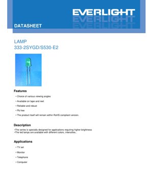
This document provides the complete technical specifications for a high-brightness bright yellow-green LED lamp bead. The device is manufactured using AlGaInP chip technology and encapsulated in green diffused resin. It is specifically designed for applications requiring reliable, robust lighting with multiple viewing angle options. This product complies with relevant environmental standards.
1.1 Core Advantages and Target Market
The main advantages of this LED series include its high luminous intensity, availability in various colors and intensities, and tape-and-reel packaging options suitable for automated assembly. It is specifically designed for applications requiring exceptional brightness. The target markets and typical applications include consumer electronics displays, indicator lights, and backlighting systems for devices such as televisions, computer monitors, telephones, and other computing equipment.
2. In-depth Technical Parameter Analysis
This section provides a detailed and objective interpretation of the key electrical, optical, and thermal parameters of the device based on standard test conditions (Ta=25°C).
2.1 Absolute Maximum Ratings
Absolute maximum ratings define stress limits that may cause permanent damage to the device. These are not recommended operating conditions.
- Continuous Forward Current (IF):25 mA. Exceeding this current continuously will shorten the LED's lifespan and reduce light output.
- Peak Forward Current (IFP):60 mA. This is the maximum allowable pulse current, typically specified under conditions of 1 kHz frequency and a duty cycle of 1/10. It is crucial for applications involving brief, high-current pulses.
- Reverse Voltage (VR):5 V. Applying a reverse bias exceeding this value may cause immediate catastrophic failure of the LED junction.
- Power Dissipation (Pd):60 mW. This is the maximum power the package can dissipate without exceeding its maximum junction temperature, calculated as the forward voltage (VF) multiplied by the forward current (IF).
- Operating and Storage Temperature:The device's rated operating temperature is -40°C to +85°C, and the storage temperature is -40°C to +100°C. These ranges ensure the mechanical and chemical stability of the epoxy resin and semiconductor materials.
- Soldering Temperature (Tsol):260°C for 5 seconds. This defines the maximum thermal profile that the LED package can withstand during wave soldering or reflow soldering processes.
2.2 Electro-Optical Characteristics
These parameters define the performance of the device under normal operating conditions (IF=20mA). The "Typical" column represents the expected median value, while the "Min" and "Max" define the acceptable production distribution range.
- Luminous Intensity (Iv):40-80 mcd (typical 80 mcd). This is the perceived brightness of the LED measured in millicandelas. The wide range indicates a binning process; designers must consider the minimum value for worst-case brightness scenarios.
- Viewing angle (2θ1/2):30 degrees (typical). This is the full angle at which the luminous intensity drops to half of its peak (axial) value. A 30-degree angle indicates a relatively concentrated beam, suitable for directional indicator lights.
- Peak and Dominant Wavelength (λp, λd):They are 575 nm and 573 nm, respectively. The peak wavelength is the spectral point of maximum radiant power. The dominant wavelength is the perceived color point. The close values indicate a spectrally pure yellow-green emission.
- Spectral Radiant Bandwidth (Δλ):20 nm. This is the spectral width at half of the maximum intensity (full width at half maximum). A bandwidth of 20 nm is typical for AlGaInP-based LEDs, providing good color purity.
- Forward Voltage (VF):1.7V to 2.4V (Typical 2.0V). This is the voltage drop across the LED when driven at 20mA. If the supply voltage is fixed, the circuit design must use a current-limiting resistor or driver calculated for the maximum VF to ensure the current does not exceed the maximum rating.
- Reverse Current (IR):Maximum 10 μA at VR=5V. This is the leakage current when the device is reverse biased. For a healthy LED, this value is typically very low.
Measurement Tolerance:The datasheet specifies particular uncertainties: ±0.1V for VF, ±10% for Iv, and ±1.0nm for λd. These must be considered in precision design calculations.
3. Explanation of the Binning System
The provided data suggests a binning structure based on key performance parameters to ensure consistency in mass production. Although the complete binning matrix is not elaborated in detail, the following information can be inferred from the specification sheet and label descriptions:
- Luminous Intensity / Luminous Flux Binning:The Iv range of 40-80 mcd indicates that the devices are binned according to their measured output at 20mA. The "CAT" field on the packaging label likely denotes this grade or category.
- Wavelength/Color Binning:The "HUE" field on the label corresponds to the dominant wavelength (λd). Given the typical value of 573 nm, production lots are likely characterized and marked according to their specific dominant wavelength to maintain color consistency within applications.
- Forward Voltage Binning:The VF range of 1.7V to 2.4V indicates that LEDs may also be grouped based on their forward voltage characteristics. Matching VF in parallel circuits helps achieve uniform current distribution.
4. Performance Curve Analysis
Typical characteristic curves provide critical insights into device behavior under various conditions, which is essential for robust circuit and thermal design.
4.1 Relative Intensity vs. Wavelength
This curve graphically represents the spectral power distribution, showing a peak near 575 nm with a full width at half maximum of approximately 20 nm. It confirms the monochromatic nature of the light output, concentrated in the yellow-green region of the visible spectrum.
4.2 Directivity Pattern
The directivity (or radiation pattern) curve illustrates the spatial distribution of light. The provided 30-degree viewing angle originates from this pattern. The curve shape is typical of standard LED chips with hemispherical lenses, showing a near-Lambertian or slightly focused emission profile.
4.3 Forward Current vs. Forward Voltage (I-V Curve)
The curve shows the exponential relationship between current and voltage, which is a typical characteristic of diodes. The "knee" voltage is approximately 1.8V-2.0V. Beyond this point, a small increase in voltage leads to a large increase in current, highlighting the extreme importance of current regulation rather than voltage regulation when driving an LED.
4.4 Relative Intensity vs. Forward Current (L-I Curve)
This curve shows the relationship between drive current and light output. It is typically linear within the recommended operating range but saturates and eventually degrades at very high currents. Operating at a typical 20mA ensures a good balance of efficiency, brightness, and lifetime.
4.5 Thermal Characteristics
The following curves are crucial:Relative Intensity vs. Ambient TemperatureandForward Current vs. Ambient Temperature(at constant voltage). They indicate that the light output decreases with increasing ambient temperature due to reduced internal quantum efficiency and increased non-radiative recombination. Conversely, for a fixed applied voltage, the forward current increases with temperature because the diode's forward voltage has a negative temperature coefficient. If not properly managed with a constant current driver, this can lead to a potential thermal runaway situation.
5. Mechanical and Packaging Information5.1 Package Dimensions and Drawings
The datasheet contains detailed dimensional drawings. Key specifications derived from the drawings and notes include: all dimensions are in millimeters (mm), the flange height must be less than 1.5mm, and unless otherwise specified, the general tolerance is ±0.25mm. The drawings define pin pitch, body dimensions, and overall shape, which are crucial for PCB pad design (pad pattern).
5.2 Polarity Identification
Although not explicitly detailed in the provided text, standard LED beads typically identify the cathode (negative pin) through a flat edge on the lens, a shorter lead, or markings on the package. The PCB pad design must match this polarity to ensure correct orientation during assembly.
6. Soldering and Assembly Guide
Proper handling is crucial for maintaining device reliability and performance.
6.1 Lead Forming
- Bending must be at least 3mm away from the epoxy lamp bead base to prevent stress cracks.
- Forming must be completed before soldering.
- Cut the leads at room temperature to avoid thermal shock.
- PCB holes must align perfectly with LED pins to avoid installation stress.
6.2 Storage Conditions
- After receipt, store at ≤30°C and ≤70% relative humidity (RH). The shelf life under these conditions is 3 months.
- For longer-term storage (up to 1 year), use a nitrogen-sealed container with a desiccant.
- Avoid sudden temperature changes in humid environments to prevent condensation.
6.3 Welding Process
Key Rules:Maintain a minimum distance of 3mm from the solder point to the epoxy resin LED.
- Manual Soldering:Maximum tip temperature 300°C (for irons up to 30W), maximum soldering time 3 seconds.
- Wave/Immersion Soldering:Preheating maximum temperature 100°C (maximum 60 seconds). Solder bath maximum temperature 260°C, maximum immersion time 5 seconds.
- The recommended soldering temperature profile is provided and should be followed to minimize thermal stress.
- Avoid applying mechanical stress to the leads during soldering and while the device is still hot after soldering.
- Do not perform more than one dip soldering/hand soldering.
- Cool gradually from the peak soldering temperature; avoid rapid quenching.
6.4 Cleaning
- Clean only when necessary, using isopropyl alcohol at room temperature, for ≤1 minute. Air dry.
- Ultrasonic cleaning is strongly discouraged. If absolutely required, extensive pre-qualification testing must be conducted to determine safe power levels and duration, as ultrasonic energy may damage internal die attach or epoxy encapsulation.
6.5 Thermal Management
Effective thermal management is crucial for the performance and lifespan of LEDs. As indicated by the derating curves referenced in the datasheet, the current rating must be appropriately reduced at higher ambient temperatures. The design must ensure that the temperature around the LED body is controlled, typically achieved by using a PCB with sufficient thermal pads, thermal vias, or an external heatsink for high-power applications.
6.6 Electrostatic Discharge (ESD) Protection
These LEDs are sensitive to electrostatic discharge. ESD may cause latent damage or immediate failure. Always handle components in an ESD-protected area using grounded wrist straps and conductive mats. Use antistatic packaging and equipment during all assembly and handling processes.
7. Packaging and Ordering Information7.1 Packaging Specifications
Device packaging is designed to prevent mechanical and electrostatic damage during transportation and handling.
- Primary Packaging:Antistatic bag.
- Secondary packaging:Inner box, containing 5 bags.
- Tertiary packaging:Outer carton, containing 10 inner boxes.
- Packaging Quantity:Minimum 200 to 500 pieces per bag. Therefore, one outer carton contains 10,000 to 25,000 pieces (10 inner boxes * 5 bags * 200-500 pieces/bag).
7.2 Labeling Instructions
The packaging label contains multiple codes for traceability and identification:
- CPN:Customer Part Number.
- P/N:Manufacturer Part Number (e.g., 333-2SYGD/S530-E2).
- QTY:Nawa a cikin jaka.
- CAT:Level or performance category (may be related to luminous intensity binning).
- HUE:Dominant wavelength code.
- REF:Reference code.
- LOT No:Production lot number, used for traceability.
8. Application Recommendations and Design Considerations8.1 Typical Application Scenarios
This LED is very suitable for:
- Status Indicator Light:Power, activity, or mode indicator lights in consumer electronics (TVs, monitors, phones, computers), due to their high brightness and focused viewing angle.
- Backlight:Edge lighting or icon backlighting for small LCD panels requiring uniform, bright illumination.
- Front panel display:Illumination for buttons, switches, or panel meters.
8.2 Key Design Considerations
- Current Limiting:Always use a series current-limiting resistor or a constant current driver. Use the maximum forward voltage (2.4V) to calculate the resistor value to ensure the current never exceeds 25mA under worst-case (minimum VF) conditions. Formula: R = (Supply Voltage - VF_max) / Target Current.
- Thermal Design:Consider the negative impact of temperature on light output and forward voltage. Provide sufficient PCB copper area or other heat dissipation means, especially in high ambient temperature environments or enclosed spaces.
- ESD Protection:Add ESD protection diodes on signal lines connected to the LED anode/cathode that are exposed to the user interface or external connectors.
- Optical Design:A 30-degree viewing angle provides a relatively narrow beam. For wider illumination, consider using a diffuser lens or selecting an LED with a wider native viewing angle.
9. Technical Comparison and Differentiation
While no direct comparison with specific competitor components is provided, according to its datasheet, the key differentiating features of this LED include:
- Chip Technology:Using AlGaInP (Aluminum Gallium Indium Phosphide) semiconductor material, which is more efficient in producing amber, yellow, and green light compared to older technologies.
- Brightness:Provides a typical luminous intensity of 80 mcd at 20mA, which is competitive in standard LED packages for this color.
- Robustness:The datasheet emphasizes a reliable and robust construction and provides detailed operating and soldering guidelines, indicating its design is intended to withstand standard assembly processes.
- Compliance:Declared as lead-free and RoHS compliant, meeting modern environmental regulations for electronic components.
10. Frequently Asked Questions (Based on Technical Parameters)
Q1: Can I drive this LED with 30mA for higher brightness?
A: A'a. Matsakaicin ƙimar ƙimar madaidaicin madaidaiciyar ci gaba ita ce 25 mA. Aiki a 30mA ya wuce wannan ƙimar, wanda zai rage rayuwar LED sosai, haifar da raguwar haske cikin sauri, kuma yana iya haifar da gazawar zafi mai ban tsoro.
Q2: Tushen wutar lantarki na shine 5V. Don ƙarfin fitarwa na 20mA, wane ƙimar juriya ya kamata in yi amfani da shi?
A: Don ƙira mai aminci, yi amfani da mafi munin yanayi (matsakaicin) ƙimar VF na 2.4V. R = (5V - 2.4V) / 0.020A = 130 ohms. Matsakaicin ƙimar daidaitaccen ƙimar juriya mafi girma shine 150 ohms. Yayin amfani da 150 ohms, ƙarfin kusan (5V - 2.0V)/150 = 20mA (ta amfani da VF na yau da kullun), wannan yana da aminci. Tabbatar da bincika amfani da wutar lantarki na resistor: P = I^2 * R = (0.02^2)*150 = 0.06W, don haka daidaitaccen resistor na 1/8W (0.125W) ya isa.
Q3: Why does the light output dim when my device gets hot?
A: This is a fundamental characteristic of LEDs, as shown in the "Relative Intensity vs. Ambient Temperature" curve. The efficiency of the semiconductor material decreases as the junction temperature rises, producing less light at the same current. Improved thermal management in the design can mitigate this effect.
Q4: Can I use ultrasonic cleaning on the PCB after soldering these LEDs?
A: Strongly not recommended. The datasheet indicates that ultrasonic cleaning may damage the LED depending on power and assembly conditions. If it must be used, you need to conduct thorough pre-qualification testing. A safer alternative is to use isopropyl alcohol with gentle brushing or to use a no-clean flux that does not require post-solder cleaning.
11. Practical Design and Use Case Studies
Scenario: Designing a set of status indicator lights for a network router.
The designer needs 5 bright yellow-green indicator lights for power, internet, Wi-Fi, and two Ethernet ports. They chose this LED for its brightness and color.
- Circuit Design:The internal logic power supply of the router is 3.3V. Using a maximum VF of 2.4V and a target current of 18mA (with added margin), the resistance value is (3.3V - 2.4V) / 0.018A = 50 ohms. A standard 51-ohm resistor is selected. The power dissipation per resistor is (0.018^2)*51 ≈ 0.0165W.
- PCB Layout:PCB pads are strictly created according to the package dimension drawing. Use small thermal relief connections to connect the LED pads to the larger ground plane to aid heat dissipation without making soldering difficult.
- Assembly:Assembly personnel follow guidelines: use ESD protection, form leads before placement (if required), and follow the recommended reflow profile with a peak temperature not exceeding 260°C.
- Result:The LED provides clear, bright indication, all five units have consistent color, and the product has passed reliability tests due to proper thermal and electrical design.
12. Brief Introduction to Working Principle
This LED operates based on the principle of electroluminescence in a semiconductor p-n junction. The chip material is AlGaInP. When a forward voltage exceeding the diode turn-on voltage (approximately 1.7-2.0V) is applied, electrons from the n-type region and holes from the p-type region are injected into the junction area. These carriers recombine in the active region of the semiconductor. A significant portion of this recombination is radiative, meaning they release energy in the form of photons (light). The specific wavelength of 573-575 nm (yellow-green) is determined by the bandgap energy of the AlGaInP alloy composition used in the chip's active layer. A green diffused epoxy package is used to protect the chip, act as the primary lens to shape the light output beam, and diffuse the light to produce a more uniform appearance.
13. Teknologi Trends and Background
This component represents the mature mainstream technology for monochromatic indicator LEDs. AlGaInP-based LEDs are the standard for efficient red, amber, and yellow-green emission. Current industry trends related to such devices include:
- Efficiency Improvement:Continuous research aims to improve the internal quantum efficiency (IQE) and light extraction efficiency (LEE) of these materials, thereby achieving higher luminous intensity at the same input current or the same brightness at lower power.
- Miniaturization:Although this is a standard LED package, the broader trend is toward smaller surface-mount device (SMD) packages (e.g., 0402, 0201) to accommodate high-density PCB designs, albeit often at the expense of total light output and thermal management capability.
- Reliability Enhancement:Improvements in epoxy formulations, die attach materials, and wire bonding technology continue to drive the operational lifetime and temperature tolerance of LEDs.
- Smart Integration:A macro trend in the lighting field is the direct integration of control circuits (drivers, communication) into the LED package, creating "smart" components. While this specific part is a discrete, non-smart LED, understanding its fundamental parameters is the basis for working with more integrated solutions.
Detailed Explanation of LED Specification Terminology
Complete Explanation of LED Technical Terminology
I. Core Indicators of Photoelectric Performance
| Terminology | Unit/Representation | Popular Explanation | Why It Matters |
|---|---|---|---|
| Luminous Efficacy | lm/W | The luminous flux emitted per watt of electrical power; higher values indicate greater energy efficiency. | Directly determines the energy efficiency rating and electricity cost of the lighting fixture. |
| Luminous Flux | lm (Lumen) | Total light output from a light source, commonly known as "brightness". | Determines if a luminaire is bright enough. |
| Viewing Angle | ° (degrees), e.g., 120° | The angle at which luminous intensity drops to half, determining the width of the light beam. | Affects the illumination range and uniformity. |
| Color Temperature (CCT) | K (Kelvin), e.g., 2700K/6500K | The warmth or coolness of light color; lower values are yellowish/warm, higher values are whitish/cool. | Determines the lighting ambiance and suitable application scenarios. |
| Color Rendering Index (CRI / Ra) | Unitless, 0–100 | The ability of a light source to restore the true color of an object, Ra≥80 is recommended. | Affects color authenticity, used in high-demand places such as shopping malls and art galleries. |
| Color tolerance (SDCM) | MacAdam ellipse steps, e.g., "5-step" | A quantitative metric for color consistency; a smaller step number indicates better color consistency. | Ensure no color variation among luminaires from the same batch. |
| Dominant Wavelength | nm (nanometer), e.g., 620nm (red) | Thamani ya urefu wa wimbi inayolingana na rangi ya LED zenye rangi. | Huamua ukoo wa rangi kwa LED za rangi moja kama nyekundu, manjano, kijani, n.k. |
| Spectral Distribution | Wavelength vs. Intensity Curve | It shows the intensity distribution of light emitted by an LED across various wavelengths. | Affects color rendering and color quality. |
II. Electrical Parameters
| Terminology | Symbol | Popular Explanation | Design Considerations |
|---|---|---|---|
| Forward Voltage | Vf | The minimum voltage required to light up an LED, similar to a "starting threshold". | The driving power supply voltage must be ≥ Vf, and the voltage accumulates when multiple LEDs are connected in series. |
| Forward Current | If | The current value that makes the LED emit light normally. | Constant current drive is often used, as current determines brightness and lifespan. |
| Maximum Pulse Current (Pulse Current) | Ifp | Peak current that can be withstood for a short period, used for dimming or flashing. | Pulse width and duty cycle must be strictly controlled to prevent overheating and damage. |
| Reverse Voltage | Vr | The maximum reverse voltage that an LED can withstand; exceeding this may cause breakdown. | The circuit must be protected against reverse connection or voltage surges. |
| Thermal Resistance | Rth (°C/W) | The resistance to heat transfer from the chip to the solder joint; a lower value indicates better heat dissipation. | High thermal resistance requires a more robust heat dissipation design; otherwise, the junction temperature will increase. |
| Electrostatic Discharge Immunity (ESD Immunity) | V (HBM), e.g., 1000V | ESD strike resistance, the higher the value, the less susceptible to ESD damage. | Anti-static measures must be implemented during production, especially for high-sensitivity LEDs. |
III. Thermal Management and Reliability
| Terminology | Key Indicators | Popular Explanation | Impact |
|---|---|---|---|
| Junction Temperature | Tj (°C) | The actual operating temperature inside the LED chip. | For every 10°C reduction, the lifespan may double; excessively high temperatures lead to lumen depreciation and color shift. |
| Lumen Depreciation | L70 / L80 (hours) | Time required for brightness to drop to 70% or 80% of its initial value. | Directly define the "useful life" of an LED. |
| Lumen Maintenance | % (e.g., 70%) | The percentage of remaining brightness after a period of use. | Characterization of luminance maintenance capability after long-term use. |
| Color Shift | Δu′v′ or MacAdam ellipse | The degree of color change during use. | Affects the color consistency of the lighting scene. |
| Thermal Aging | Material performance degradation | Degradation of packaging materials due to prolonged high temperatures. | May lead to decreased brightness, color changes, or open-circuit failure. |
IV. Packaging and Materials
| Terminology | Common Types | Popular Explanation | Features and Applications |
|---|---|---|---|
| Package Types | EMC, PPA, Ceramic | A housing material that protects the chip and provides optical and thermal interfaces. | EMC has good heat resistance and low cost; ceramic has excellent heat dissipation and long lifespan. |
| Chip Structure | Front Side, Flip Chip | Chip electrode arrangement method. | Flip Chip offers better heat dissipation and higher luminous efficacy, suitable for high-power applications. |
| Phosphor coating | YAG, silicate, nitride | Coated on the blue LED chip, partially converted to yellow/red light, mixed to form white light. | Different phosphors affect luminous efficacy, color temperature, and color rendering. |
| Lens/Optical Design | Planar, microlens, total internal reflection | Optical structure on the encapsulation surface, controlling light distribution. | Determines the emission angle and light distribution curve. |
V. Quality Control and Binning
| Terminology | Binning Content | Popular Explanation | Purpose |
|---|---|---|---|
| Luminous flux binning | Codes such as 2G, 2H | Group by brightness level, each group has a minimum/maximum lumen value. | Ensure consistent brightness for products within the same batch. |
| Voltage binning | Codes such as 6W, 6X | Grouped according to forward voltage range. | Facilitates driver power matching and improves system efficiency. |
| Color binning | 5-step MacAdam ellipse | Group by color coordinates to ensure colors fall within an extremely small range. | Ensure color consistency to avoid color unevenness within the same luminaire. |
| Color temperature binning | 2700K, 3000K, etc. | Group by color temperature, each group has a corresponding coordinate range. | Meet the color temperature requirements of different scenarios. |
VI. Testing and Certification
| Terminology | Standards/Testing | Popular Explanation | Significance |
|---|---|---|---|
| LM-80 | Lumen Maintenance Test | Long-term operation under constant temperature conditions, recording data on brightness attenuation. | Used for estimating LED lifespan (combined with TM-21). |
| TM-21 | Life Extrapolation Standard | Estimating lifespan under actual use conditions based on LM-80 data. | Providing scientific life prediction. |
| IESNA Standard | Illuminating Engineering Society Standard | Covering optical, electrical, and thermal testing methods. | Industry-recognized testing basis. |
| RoHS / REACH | Environmental Certification | Ensure products are free from hazardous substances (e.g., lead, mercury). | Conditions for market entry into the international market. |
| ENERGY STAR / DLC | Energy efficiency certification. | Energy Efficiency and Performance Certification for Lighting Products. | Commonly used in government procurement and subsidy programs to enhance market competitiveness. |