Table of Contents
- 1. Product Overview
- 2. Detailed Technical Parameters
- 2.1 Absolute Maximum Ratings
- 2.2 Electrical Characteristics
- 2.2.1 Input Characteristics
- 2.2.2 Output and Transmission Characteristics
- 2.3 Switching Characteristics
- 3. Performance Curve Analysis
- 4. Mechanical and Packaging Information
- 4.1 Pin Configuration
- 5. Welding and Assembly Guide
- 6. Application Recommendations
- 6.1 Typical Application Circuit
- 6.2 Design Considerations
- 7. Technical Comparison and Differentiation
- 8. Frequently Asked Questions (Based on Technical Parameters)
- 9. Working Principle
- 10. Industry Trends and Background
1. Product Overview
The EL063X series is a class of dual-channel high-speed logic gate optocouplers (optical isolators). These devices are designed to provide robust electrical isolation and high-speed digital signal transmission between two circuits. Their core function is to transmit logic-level signals across an isolation barrier through optical coupling between an infrared light-emitting diode (LED) and a high-speed integrated photodetector with logic gate output. This design effectively eliminates ground loops, prevents noise transmission, and protects sensitive circuits from voltage spikes or ground potential differences.
The primary application areas for this component include industrial automation, communication interfaces, power supply control, and computer peripherals, where reliable, noise-immune signal transmission is critical. The dual-channel configuration within a single package offers space-saving advantages for differential signal applications or multi-channel control line isolation and ensures consistency in channel characteristics.
2. Detailed Technical Parameters
Electrical and optical parameters define the operating boundaries and performance of the optocoupler.
2.1 Absolute Maximum Ratings
These are stress limits that must not be exceeded under any conditions, even momentarily. Operating beyond these ratings may cause permanent damage to the device.
- Input Forward Current (IF)): 20 mA DC/average. This limits the maximum current through the input LED.
- Input reverse voltage (VR)): 5 V. The maximum reverse bias voltage that the input LED can withstand.
- Output current (IO)): 50 mA. The maximum current that the output transistor can sink.
- Output voltage (VO) with power supply voltage (VCC)): 7.0 V. The maximum voltage that can be applied to the output side pins.
- Isolation voltage (VISO)):3750 VEffective value, lasting for 1 minute. This is a critical safety parameter indicating the dielectric strength of the isolation barrier between the input and output sides. During the test, pins 1-4 are shorted together, and pins 5-8 are shorted together.
- Operating Temperature (TOPR)): -40°C to +100°C. The ambient temperature range within which the device is guaranteed to operate normally.
- Storage Temperature (TSTG)):-55°C to +125°C.
2.2 Electrical Characteristics
These parameters are guaranteed under the specified operating conditions (unless otherwise noted, Ta = -40°C to 85°C).
2.2.1 Input Characteristics
- Forward voltage (VF)): Typical value 1.4V, maximum 1.8V at IF= 10 mA. Used to calculate the series resistor required for the input LED drive circuit.
- VFTemperature coefficient: Approximately -1.8 mV/°C. LED forward voltage decreases as temperature increases.
- Input capacitance (CIN)): Typical value 60 pF. This parasitic capacitance affects the high-frequency performance on the input side.
2.2.2 Output and Transmission Characteristics
- Power supply current (ICCH/ICCL)): Output IC static current consumption. ICCH(Output high level) Typical value is 13 mA (maximum 18 mA). At VCCL= 5.5V时,ICC(Output low level) Typical value is 15 mA (max 21 mA). This is important for power budget calculation.
- High-level output current (IOH)): When the output maintains a high logic level (VOclose to VCC), it can provide a maximum current of 100 µA. This is a relatively weak current sourcing capability.
- Low-level output voltage (VOL)): in IF= 5mA and ICL= 13mA, maximum 0.6V. This defines the voltage level when the output transistor actively sinks current, ensuring compatibility with TTL/CMOS logic low-level thresholds.
- Input threshold current (IFT)): Maximum 5 mA. This is the input current required to guarantee the output switches to a valid low-level state (VO≤ 0.6V) under specified conditions. Designers must ensure the driving circuit provides at least this current to achieve reliable switching.
2.3 Switching Characteristics
These parameters define high-speed digital performance, measured under standard test conditions (Ta=25°C, VCC=5V, IF=7.5mA, CL=15pF, RL=350Ω).
- Propagation delay (tPHL, tPLH)): Each maximum 100 ns. tPHLis the delay from the input LED turning on (current rising) to the output falling. tPLHIt is the delay from the input LED turning off (current falling) to the output rising. These delays limit the maximum data rate.
- Pulse Width Distortion (|tPHL– tPLH|): Maximum 35 ns. This asymmetry between the rise and fall delays distorts the duty cycle of the transmitted pulse, which is critical in timing-sensitive applications.
- Output rise/fall time (tr, tf)): trTypical value is 40 ns (10% to 90%), tfTypical value is 10 ns (90% to 10%). A faster fall time is characteristic of the active pull-down output stage.
- Common-Mode Transient Immunity (CMTI): This is a key parameter for noise immunity in noisy environments such as motor drives or switching power supplies. It measures the device's ability to suppress fast voltage transients appearing across the isolation barrier.
- EL0630: Minimum 5000 V/µs.
- EL0631: Minimum 10000 V/µs. The higher CMTI makes the EL0631 suitable for applications with more severe electrical noise.
- This suppression capability is for the output high level (CMH) and the output low level (CMLThe states are all specified to ensure that the output does not falsely trigger during transient events.
3. Performance Curve Analysis
Although the provided PDF excerpt mentions "typical photoelectric characteristic curves," the specific charts are not included in the text. Typically, such curves for optocouplers include:
- Current Transfer Ratio (CTR) versus Forward Current (IF)Relationship: Shows the efficiency of optocoupler (output current / input current) under different drive levels.
- Propagation Delay versus Forward Current (IF)Relationship: Illustrates how switching speed varies with LED drive current. Higher IFgenerally reduces propagation delay.
- Relationship between propagation delay and temperature: Shows the temperature dependence of switching speed.Relationship between output saturation voltage and output current: Characterizes the performance of the output transistor when sinking current.
- Designers should consult the complete datasheet containing graphs to understand these relationships and optimize their specific application, such as making trade-offs between speed and LED current/power consumption.4. Mechanical and Packaging Information
The device employs a standard 8-pin small outline package (SOP or SOIC). This surface-mount package conforms to the common SO8 package dimensions, facilitating PCB layout and assembly.
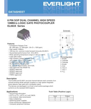
4.1 Pin Configuration
The pin configuration is as follows:
Pin 1: Anode (Channel 1 input LED)
Pin 2: Cathode (Channel 1 input LED)
- Pin 3: Cathode (Channel 2 Input LED)
- Pin 4: Anode (Channel 2 Input LED)
- Pin 5: Ground (GND) - Output Side Common Terminal.
- Pin 6: V
- 2 (Channel 2 output)
- Pin 7: VOUT1 (Channel 1 Output)
- Pin 8: VOUT(Output side power supply voltage, typical value +5V)
- Important Note:CCInput and output sides are fully isolated. Pins 1-4 are on the isolated input side, and pins 5-8 are on the isolated output side. PCB layout must maintain sufficient creepage distance and electrical clearance between the two sets of pins and their associated traces to maintain the isolation rating.
5. Welding and Assembly GuideThe device is suitable for standard surface-mount assembly processes.
Soldering temperature: The maximum allowable soldering temperature is 260°C for 10 seconds. This is compatible with typical lead-free reflow soldering temperature profiles.
Moisture Sensitivity: Although not explicitly stated in the excerpt, most plastic-encapsulated SMD devices have a Moisture Sensitivity Level (MSL). To prevent "popcorn" phenomenon during reflow soldering, proper handling, baking (if required), and storage according to the manufacturer's guidelines are essential.
- Output bypass: A critical design note (*3) specifies that VThe power supply pin (8) must be bypassed with a 0.1 µF or larger capacitor (ceramic or solid tantalum with good high-frequency characteristics). This capacitor must be placed as close as possible to pin 8 (V
- ) and pin 5 (GND) to ensure stable operation and minimize switching noise on the supply rail.6. Application Recommendations
- 6.1 Typical Application CircuitThe datasheet lists several key applications:CCGround Loop Elimination: Primary function, isolating the grounds of two subsystems to prevent circulating currents and noise.CCLogic Level Conversion/Interface: Can interface between different logic families (e.g., from LSTTL to TTL or 5V CMOS) while providing isolation.
Data Transmission and Line Receivers: Suitable for isolated serial data links (e.g., RS-232, RS-485 isolation), digital I/O isolation, and multiplexing.
Switched-mode power supply feedback: In flyback or other isolated converter topologies, isolates the feedback signal from the secondary (output) side to the primary (controller) side.
Pulse transformer replacement: Provides a solid-state, potentially more reliable and compact alternative for transmitting digital pulses across an isolation barrier.
- Computer peripheral device interface: Isolate signals between printers, industrial I/O cards, or other peripheral devices.6.2 Design Considerations
- Input drive circuit: Must be based on the input power supply voltage (V), required forward current I
- and V of the LEDto calculate the series resistor. R
- Series= (V
- - V) / I
- . To ensure reliable switching, Imust be ≥ I
, and can be increased to the absolute maximum rating to improve speed, at the cost of higher power consumption.
- Output load: The output is designed to drive standard logic loads. Pull-up resistor R(connected between VINand the output pin) sets the logic high level and rise time. A smaller RFprovides a faster rise time but increases power consumption when the output is low. Test conditions use RF=350Ω.Power consumption: Calculate input side (P= VIN* IF) and the total power consumption on the output side, ensuring it remains within the specified limits, especially under high-temperature conditions.FChannel Selection: For applications requiring higher common-mode noise immunity (CMTI ≥ 10,000 V/µs compared to 5,000 V/µs), choose EL0631 instead of EL0630.F7. Technical Comparison and DifferentiationFTThe EL063X series stands out in the market through the following key features:
- High Speed: With a capability of 10 Mbit/s and a propagation delay of ≤100 ns, it belongs to the high-speed optocoupler category, suitable for fast digital communication.SOP-8 Package Dual Channel: Integrates two isolated channels in a compact standard package, saving board space compared to two single-channel devices.LHigh CMTI: Particularly the minimum 10 kV/µs CMTI of the EL0631 offers significant advantages in electrically noisy environments like industrial motor drives, where optocouplers with low CMTI may fail.CCWide Temperature Range: Guaranteed performance from -40°C to 85°C, with an operating range up to 100°C, suitable for industrial and automotive applications.LComprehensive Safety Approvals: The device is certified by major international safety agencies (UL, cUL, VDE, SEMKO, etc.), which is often a mandatory requirement for end products in regulated markets.LEnvironmental Compliance: Halogen-free (Br/Cl restrictions), lead-free, compliant with RoHS and REACH standards, meeting modern environmental regulations.
- 8. Frequently Asked Questions (Based on Technical Parameters)Q: What is the maximum data rate achievable using this optocoupler?DA: The specification of 10 Mbit/s and a maximum propagation delay of 100 ns suggest a maximum theoretical data rate of approximately 5-10 Mbps for NRZ data. In practice, the achievable rate depends on specific waveforms, rise/fall times, and pulse width distortion. For reliable operation, a conservative design target is typically 1-5 Mbps.FQ: How to choose between EL0630 and EL0631?FA: The main difference lies in the Common-Mode Transient Immunity (CMTI). If your application involves significant switching noise (e.g., near motor drivers, high-power inverters, noisy power supplies), the EL0631 (10 kV/µs) offers superior noise immunity. For less noisy environments, the EL0630 (5 kV/µs) may be sufficient.
- Q: Why does Vrequire a bypass capacitor?
A: The high-speed switching of the output stage can cause noise on the V
line. The local bypass capacitor provides a low-impedance source for this current, preventing the V
- from experiencing voltage droops or spikes, which could otherwise lead to operational instability or noise radiation. Placing it close to the pin is crucial for effectiveness.Q: Can I use this device to isolate analog signals?
- A: No. This is alogic gate
- optocoupler. The output is a digital logic level (high or low), not a linear representation of the input current. For analog isolation, a linear optocoupler (with a phototransistor or photodiode output) is required.Q: What is the purpose of the "triggerable output" mentioned in the description?
- A: Although not detailed in this excerpt, a triggerable output typically means the output stage has an enable or trigger control. This allows the output to be turned on/off or latched via a third control signal, which is useful in multiplexing applications or for reducing power consumption. The pin configuration here does not show a separate trigger pin, so this function may be internally integrated in a specific mode, or it may refer to the output being enabled by the input signal itself.9. Working Principle
- The operating principle is based on photoelectric conversion. When sufficient forward current (I) is applied to the input infrared light-emitting diode (IRED), it emits photons. These photons pass through a transparent isolation barrier (typically a molded plastic compound). On the output side, a high-speed silicon photodetector integrated circuit receives this light. This IC contains a photodiode that converts the light back into a photocurrent. This photocurrent is then processed by internal amplifier and comparator circuits ("logic gates") to produce a clean, well-defined digital output voltage. When the input LED is on, the output is driven to a logic low state (typically via an active pull-down transistor). When the input LED is off, the output circuit pulls the pin to a logic high state (via an external pull-up resistor R
- ). This positive logic operation is summarized in the provided truth table as: input high = output low, input low = output high.10. Industry Trends and Background
The development of optocouplers such as the EL063X series is driven by several key trends in the field of electronics:
Demand for higher speed and bandwidth: With the increasing speed of industrial networks (EtherCAT, PROFINET IRT) and communication interfaces, isolators must keep pace. The trend from kilobits to megabits, and now to 10+ megabit speeds is evident.
Enhanced noise immunity: The growing electrical complexity of industrial and automotive environments requires isolators with higher CMTI ratings to ensure reliable operation amidst noise generated by motor drives, switching power supplies, and RF sources.
Miniaturization and integration: The dual-channel design in SOP-8 packages reflects the need to save PCB space and reduce component count. Further trends include integrating more channels (quad-channel isolators) or combining isolation with other functions (such as ADC drivers or I
C level shifting).
Higher Safety and Reliability Standards: Stricter safety regulations across industries are driving demand for components with higher isolation voltages, longer operational lifetimes, and robust certifications from bodies like UL, VDE, and CQC.CC?
Alternative Isolation Technologies: While optocoupler technology is mature, they face competition from capacitive isolators (using SiOCCbarriers) and magnetic isolators (giant magnetoresistance or transformer-based), which may offer advantages in speed, power consumption, and integration density. However, optocouplers maintain a solid position due to their high CMTI, simplicity, and well-understood reliability.CCEL063X series, with its balance of speed, dual-channel integration, high CMTI, and safety certifications, is designed to meet the market's ongoing demand for robust, high-performance signal isolation.
Q: Can I use this device to isolate analog signals?
A: No. This is alogic gatephotocoupler. The output is a digital logic level (high or low), not a linear representation of the input current. For analog isolation, a linear optocoupler (with a phototransistor or photodiode output) is required.
Q: What is the purpose of the "strobable output" mentioned in the description?
A> While not detailed in this excerpt, a strobable output typically means the output stage has an enable or strobe control. This allows the output to be turned on/off or latched by a third control signal, which can be useful for multiplexing applications or reducing power consumption. The pin configuration here does not show a separate strobe pin, so this functionality may be integrated internally in a specific mode or may refer to the output being enabled by the input signal itself.
. Operational Principle
The operational principle is based on optoelectronic conversion. When a sufficient forward current (IF) is applied to the input Infrared Emitting Diode (IRED), it emits light photons. These photons traverse the transparent isolation barrier (typically a molded plastic compound). On the output side, a high-speed silicon photodetector integrated circuit receives this light. This IC contains a photodiode that converts the light back into a photocurrent. This photocurrent is then processed by an internal amplifier and comparator circuit (the "logic gate") to produce a clean, well-defined digital output voltage. When the input LED is ON, the output is driven to a logic LOW state (typically by an active pull-down transistor). When the input LED is OFF, the output circuit pulls the pin to a logic HIGH state (through the external pull-up resistor RL). This positive logic operation is summarized in the provided Truth Table: Input High = Output Low, Input Low = Output High.
. Industry Trends & Context
The development of photocouplers like the EL063X series is driven by several key trends in electronics:
- Demand for Higher Speed and Bandwidth: As industrial networks (EtherCAT, PROFINET IRT) and communication interfaces speed up, isolators must keep pace. The move from kilobit to megabit and now towards 10+ megabit speeds is evident.
- Increased Noise ImmunityIndustrial and automotive environments are becoming more electrically complex, necessitating isolators with higher CMTI ratings to ensure reliable operation amidst noise from motor drives, switching power supplies, and RF sources.
- Miniaturization and IntegrationThe dual-channel design in an SOP-8 package reflects the need to save PCB real estate and reduce component count. Further trends include integrating more channels (quad isolators) or combining isolation with other functions like ADC drivers or I2C level translation.
- Enhanced Safety and Reliability StandardsStricter safety regulations across industries push for components with higher isolation voltages, longer operational lifetimes, and robust certifications from agencies like UL, VDE, and CQC.
- Alternative Isolation TechnologiesWhile optocouplers are mature, they face competition from capacitive isolators (using SiO2barriers) and magnetic (giant magnetoresistance or transformer-based) isolators, which can offer advantages in speed, power consumption, and integration density. However, optocouplers maintain strong positions due to their high CMTI, simplicity, and well-understood reliability.
The EL063X series, with its balance of speed, dual-channel integration, high CMTI, and safety certifications, is positioned to address these ongoing demands in the market for robust, high-performance signal isolation.
LED Specification Terminology Explained
Complete Explanation of LED Technical Terms
I. Core Indicators of Photoelectric Performance
| Terminology | Unit/Representation | Layman's Explanation | Why is it important |
|---|---|---|---|
| Luminous Efficacy | lm/W | The luminous flux emitted per watt of electrical power; the higher the value, the more energy-efficient. | It directly determines the energy efficiency rating and electricity cost of the luminaire. |
| Luminous Flux | lm (Lumen) | The total amount of light emitted by a light source, commonly known as "brightness". | Determines whether the luminaire is bright enough. |
| Viewing Angle | ° (degree), such as 120° | The angle at which light intensity drops to half, determining the beam width. | Affects the illumination range and uniformity. |
| Color Temperature (CCT) | K (Kelvin), e.g., 2700K/6500K | The color temperature of light, lower values lean yellow/warm, higher values lean white/cool. | Determines the lighting ambiance and suitable application scenarios. |
| Color Rendering Index (CRI / Ra) | Unitless, 0–100 | The ability of a light source to reproduce the true colors of objects, with Ra≥80 being preferable. | Affects color fidelity, used in high-demand places such as shopping malls and art galleries. |
| Color tolerance (SDCM) | MacAdam ellipse steps, such as "5-step" | A quantitative metric for color consistency; a smaller step number indicates better color consistency. | Ensure no color variation among luminaires from the same batch. |
| Dominant Wavelength | nm (nanometer), e.g., 620nm (red) | The wavelength value corresponding to the color of a colored LED. | Determines the hue of monochromatic LEDs such as red, yellow, and green. |
| Spectral Distribution | Wavelength vs. Intensity curve | Shows the intensity distribution of light emitted by an LED at various wavelengths. | Affects color rendering and color quality. |
II. Electrical Parameters
| Terminology | Symbol | Layman's Explanation | Design Considerations |
|---|---|---|---|
| Forward Voltage (Forward Voltage) | Vf | The minimum voltage required to light up an LED, similar to a "starting threshold". | The driving power supply voltage must be ≥ Vf, and the voltage adds up when multiple LEDs are connected in series. |
| Forward Current | If | The current value that makes the LED emit light normally. | Constant current drive is often used, as the current determines brightness and lifespan. |
| Maximum Pulse Current | Ifp | Peak current that can be withstood for a short period of time, used for dimming or flashing. | Pulse width and duty cycle must be strictly controlled, otherwise overheating damage will occur. |
| Reverse Voltage | Vr | Maximum reverse voltage an LED can withstand; exceeding it may cause breakdown. | Reverse connection or voltage surges must be prevented in the circuit. |
| Thermal Resistance | Rth (°C/W) | The resistance to heat flow from the chip to the solder joint. A lower value indicates better heat dissipation. | High thermal resistance requires a stronger heat dissipation design, otherwise the junction temperature will increase. |
| Electrostatic Discharge Immunity (ESD Immunity) | V (HBM), such as 1000V | Electrostatic discharge immunity, higher value indicates greater resistance to electrostatic damage. | Anti-static measures must be implemented during production, especially for high-sensitivity LEDs. |
III. Thermal Management and Reliability
| Terminology | Key Indicators | Layman's Explanation | Impact |
|---|---|---|---|
| Junction Temperature | Tj (°C) | The actual operating temperature inside the LED chip. | For every 10°C reduction, the lifespan may double; excessively high temperatures lead to lumen depreciation and color shift. |
| Lumen Depreciation | L70 / L80 (hours) | The time required for the brightness to drop to 70% or 80% of its initial value. | Directly define the "service life" of LED. |
| Lumen Maintenance | % (e.g., 70%) | The percentage of remaining brightness after a period of use. | Characterizes the ability to maintain brightness after long-term use. |
| Color Shift | Δu′v′ or MacAdam Ellipse | The degree of color change during use. | Affects the color consistency of the lighting scene. |
| Thermal Aging | Material performance degradation | Degradation of packaging materials due to prolonged high temperatures. | May lead to decreased brightness, color shift, or open-circuit failure. |
IV. Packaging and Materials
| Terminology | Common Types | Layman's Explanation | Features and Applications |
|---|---|---|---|
| Package Type | EMC, PPA, Ceramic | The housing material that protects the chip and provides optical and thermal interfaces. | EMC has good heat resistance and low cost; ceramics offer superior heat dissipation and long lifespan. |
| Chip Structure | Face-up, Flip Chip | Chip Electrode Layout Method. | Flip-chip offers better heat dissipation and higher luminous efficacy, suitable for high-power applications. |
| Phosphor coating | YAG, silicate, nitride | Covered on the blue light chip, partially converted into yellow/red light, mixed into white light. | Different phosphors affect luminous efficacy, color temperature, and color rendering. |
| Lens/Optical Design | Flat, microlens, total internal reflection | The optical structure on the encapsulation surface controls the distribution of light. | It determines the light emission angle and the light distribution curve. |
V. Quality Control and Binning
| Terminology | Grading Content | Layman's Explanation | Purpose |
|---|---|---|---|
| Luminous flux binning | Codes such as 2G, 2H | Grouped by brightness level, each group has a minimum/maximum lumen value. | Ensure consistent brightness within the same batch of products. |
| Voltage binning | Codes such as 6W, 6X | Group by forward voltage range. | Facilitates driver power matching and improves system efficiency. |
| Color binning | 5-step MacAdam ellipse | Group by color coordinates to ensure colors fall within an extremely narrow range. | Ensure color consistency to avoid uneven color within the same luminaire. |
| Color temperature binning | 2700K, 3000K, etc. | Group by color temperature, each group has a corresponding coordinate range. | To meet the color temperature requirements of different scenarios. |
VI. Testing and Certification
| Terminology | Standard/Test | Layman's Explanation | Meaning |
|---|---|---|---|
| LM-80 | Lumen Maintenance Test | Long-term operation under constant temperature conditions, recording brightness attenuation data. | Used to estimate LED lifetime (combined with TM-21). |
| TM-21 | Lifetime extrapolation standard | Estimating lifespan under actual operating conditions based on LM-80 data. | Providing scientific lifespan prediction. |
| IESNA standard | Illuminating Engineering Society Standard | Covers optical, electrical, and thermal test methods. | Industry-recognized testing basis. |
| RoHS / REACH | Environmental certification. | Ensure products are free from harmful substances (e.g., lead, mercury). | Entry requirements for the international market. |
| ENERGY STAR / DLC | Energy Efficiency Certification | Energy efficiency and performance certification for lighting products. | Commonly used in government procurement and subsidy programs to enhance market competitiveness. |