Table of Contents
- 1. Product Overview
- 2. In-Depth Technical Parameter Analysis
- 2.1 Photometric and Electrical Characteristics
- 2.2 Thermal Characteristics
- 3. Absolute Maximum Ratings
- 4. Performance Curve Analysis
- 4.1 Wavelength and Spectral Distribution
- 4.2 Forward Current vs. Forward Voltage (I-V Curve)
- 4.3 Relative Luminous Flux vs. Forward Current
- 4.4 Temperature Dependence
- 4.5 Forward Current Derating Curve
- 5. Binning System Explanation
- 5.1 Luminous Flux Binning
- 5.2 Forward Voltage Binning
- 5.3 Color (Chromaticity) Binning
- 6. Part Number and Ordering Information
- 7. Mechanical, Assembly, and Packaging
- 7.1 Mechanical Dimensions
- 7.2 Recommended Soldering Pad Layout
- 7.3 Reflow Soldering Profile
- 7.4 Packaging Information
- 8. Application Guidelines and Design Considerations
- 8.1 Precautions for Use
- 8.2 Sulfur Robustness
- 8.3 Compliance Information
- 9. Technical Comparison and Differentiation
- 10. Frequently Asked Questions (Based on Technical Parameters)
- 11. Design and Usage Case Study
- 12. Operating Principle
- 13. Technology Trends
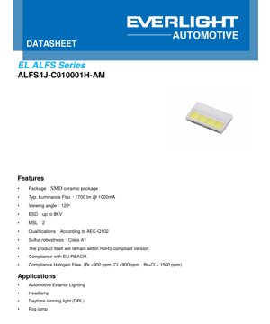
1. Product Overview
The ALFS4J-C010001H-AM is a high-power, surface-mount LED designed specifically for demanding automotive exterior lighting applications. It is built using a robust ceramic package, offering superior thermal management and reliability under harsh environmental conditions. The device is engineered to meet the stringent requirements of the automotive industry.
Core Advantages: The primary advantages of this LED include its high typical luminous flux output of 1700 lumens at a drive current of 1000mA, a wide 120-degree viewing angle for excellent light distribution, and robust construction that includes ESD protection up to 8kV. Its qualification according to AEC-Q102 standards and sulfur robustness (Class A1) make it suitable for long-term use in automotive environments where exposure to corrosive elements is common.
Target Market & Applications: This LED is targeted exclusively at automotive exterior lighting systems. Its key applications include primary headlamps, daytime running lights (DRL), and fog lamps. The combination of high brightness and reliability makes it an ideal choice for safety-critical lighting functions that require consistent performance over a wide temperature range and throughout the vehicle's lifespan.
2. In-Depth Technical Parameter Analysis
2.1 Photometric and Electrical Characteristics
The electrical and optical performance is defined under specific test conditions, primarily at a forward current (IF) of 1000mA and a thermal pad temperature of 25°C.
- Luminous Flux (Φv): The typical value is 1700 lm, with a minimum of 1500 lm and a maximum of 2000 lm. It is crucial to note the measurement tolerance of ±8%. This parameter is highly dependent on junction temperature.
- Forward Voltage (VF): The typical forward voltage is 13V, ranging from a minimum of 11.6V to a maximum of 15.2V at 1000mA, with a tight measurement tolerance of ±0.05V. This parameter directly impacts the driver design and power dissipation.
- Forward Current (IF): The device is rated for a continuous forward current up to 1500mA, with a typical operating point at 1000mA. All photometric data is specified at this typical current.
- Viewing Angle (φ): The nominal viewing angle is 120 degrees, with a tolerance of ±5°. This wide angle is beneficial for applications requiring broad illumination patterns.
- Color Temperature (K): The correlated color temperature (CCT) ranges from 5391K to 6893K, classifying it as a cool white LED. The exact binning structure is detailed later.
2.2 Thermal Characteristics
Effective thermal management is critical for LED performance and longevity. This LED provides two key thermal resistance parameters.
- Thermal Resistance, Junction to Solder (RthJS): Two values are given: RthJS_real (typical 1.26 K/W, max 1.6 K/W) and RthJS_el (typical 0.8 K/W, max 1 K/W). The "real" value represents the actual thermal path, while the "el" value is an electrical equivalent used for certain modeling purposes. A lower thermal resistance allows for more efficient heat transfer from the LED junction to the printed circuit board (PCB).
3. Absolute Maximum Ratings
Exceeding these limits may cause permanent damage to the device. Designers must ensure operating conditions remain within these boundaries.
- Power Dissipation (Pd): 22800 mW
- Forward Current (IF): 1500 mA (DC)
- Junction Temperature (Tj): 150 °C
- Operating Temperature (Topr): -40 °C to +125 °C
- Storage Temperature (Tstg): -40 °C to +125 °C
- ESD Sensitivity (HBM): 8 kV (R=1.5kΩ, C=100pF)
- Reflow Soldering Temperature: 260 °C (peak)
The device is not designed for reverse voltage operation. The high ESD rating is essential for handling and assembly in automotive production environments.
4. Performance Curve Analysis
4.1 Wavelength and Spectral Distribution
The relative spectral distribution graph shows the light output as a function of wavelength. For a cool white LED, the spectrum typically features a strong blue peak from the LED chip itself and a broader yellow/red emission from the phosphor coating. The exact shape determines the color rendering properties and the precise white point (chromaticity coordinates). The graph is measured at 25°C case temperature and 1000mA.
4.2 Forward Current vs. Forward Voltage (I-V Curve)
This graph is fundamental for driver design. It shows the relationship between the current flowing through the LED and the voltage drop across it. The curve is non-linear. At the typical 1000mA operating point, the voltage is approximately 13V. Designers use this curve to calculate the necessary driver output voltage and to understand power dissipation (VF * IF).
4.3 Relative Luminous Flux vs. Forward Current
This graph illustrates how light output increases with drive current. The relationship is generally sub-linear; doubling the current does not double the light output due to efficiency droop and increased junction temperature. The graph is normalized to the flux at 1000mA. It helps designers choose the optimal drive current to balance brightness, efficiency, and device lifetime.
4.4 Temperature Dependence
Several graphs detail the impact of temperature on LED performance, all measured at a constant 1000mA drive current.
- Relative Forward Voltage vs. Junction Temperature: The forward voltage decreases linearly as junction temperature increases. This property can sometimes be used to estimate the junction temperature.
- Relative Luminous Flux vs. Junction Temperature: Light output decreases as temperature rises. This graph quantifies that reduction, which is critical for thermal design. Maintaining a low junction temperature is essential for achieving consistent brightness.
- Chromaticity Shift vs. Junction Temperature: The color coordinates (CIE x, y) shift with temperature. This graph shows the delta (Δ) change from the value at 25°C. Minimizing this shift is important for applications requiring stable color appearance.
- Chromaticity Shift vs. Forward Current: Similarly, color coordinates can shift with drive current, even at a constant temperature.
4.5 Forward Current Derating Curve
This is one of the most critical graphs for reliable system design. It shows the maximum allowable forward current as a function of the solder point (or case) temperature. As the ambient or board temperature increases, the maximum safe current decreases to prevent the junction temperature from exceeding its 150°C limit. Designers must use this curve to select appropriate drive currents for their specific thermal environment.
5. Binning System Explanation
Due to manufacturing variations, LEDs are sorted into performance bins to ensure consistency within a production lot. This device uses a multi-parameter binning system.
5.1 Luminous Flux Binning
LEDs are grouped by their measured luminous flux at the typical forward current. The bin structure uses a combination of a Group letter and a Bin number.
- Group E: Includes bins 7 (1500-1600 lm), 8 (1600-1700 lm), and 9 (1700-1800 lm).
- Group F: Incluye los bins 0 (1800-1900 lm) y 1 (1900-2000 lm).
El ALFS4J-C010001H-AM tiene un flujo típico de 1700 lm, ubicándolo en el Bin 9 del Grupo E. La tolerancia de medición es ±8%.
5.2 Forward Voltage Binning
LEDs are also sorted by their forward voltage at the typical current. This helps in designing parallel strings and managing power supply requirements.
- Bin 4A: VF = 11.60V to 12.80V
- Bin 4B: VF = 12.80V to 14.00V
- Bin 4C: VF = 14.00V to 15.20V
The typical VF of 13V suggests the device falls within Bin 4B. The measurement tolerance is ±0.05V.
5.3 Color (Chromaticity) Binning
E binning structures are presented for color coordinates on the CIE 1931 chromaticity diagram: ECE and an alternative structure.
ECE Bin Structure: This appears to be a multi-segment bin structure for cool white LEDs. Specific bins like 63M, 61M, 58M, and 56M are defined by quadrilaterals on the CIE chart, each with four sets of (x, y) coordinates that define its corners. This allows for tighter color control by grouping LEDs with very similar chromaticity. The typical color temperature range of 5391K to 6893K spans these bins. The measurement tolerance for coordinates is ±0.005.
Alternative Structure: Another set of bins (65L, 65H, 61L, 61H) is shown, likely representing a different sorting standard or internal classification, also for cool white LEDs.
6. Part Number and Ordering Information
The part number is ALFS4J-C010001H-AM. While the full ordering information including packaging quantities (e.g., tape and reel specifications) is referenced in the document's table of contents, the specific details are not provided in the excerpt. Typically, such information would include reel size, orientation, and quantity per reel.
7. Mechanical, Assembly, and Packaging
7.1 Mechanical Dimensions
LED e fa'aaogaina se Surface-Mount Device (SMD) ceramic package. O le fua tonu (umi, lautele, maualuga, lapo'a pad, ma tolerances) o lo'o i totonu o le vaega "Mechanical Dimension". O pusa sima e ofoina atu le lelei o le vevela ma le mautu faʻainisinia pe a faʻatusatusa i pusa palasitika, lea e taua tele mo faʻaoga maualuga-malosi ma le faʻamaoni i lalo o le taamilosaga vevela.
7.2 Recommended Soldering Pad Layout
A recommended footprint for the PCB is provided. This includes the size, shape, and spacing of the copper pads for the electrical terminals and, crucially, the thermal pad. A properly designed thermal pad with adequate vias to inner ground planes or a heatsink is essential for transferring heat away from the LED to maintain low junction temperature and ensure performance.
7.3 Reflow Soldering Profile
The document specifies a reflow soldering profile with a peak temperature of 260°C. The profile details (preheat, soak, reflow, and cooling times and temperatures) are critical for achieving reliable solder joints without damaging the LED component. Adherence to this profile is necessary to prevent thermal shock, delamination, or degradation of internal materials.
7.4 Packaging Information
Details on how the LEDs are supplied (e.g., embossed tape width, pocket dimensions, reel diameter, and orientation) would be found here. This information is necessary for setting up automated pick-and-place assembly equipment.
8. Application Guidelines and Design Considerations
8.1 Precautions for Use
General handling and design warnings are provided to ensure reliability. Key precautions likely include:
- ESD Protection: Despite the 8kV HBM rating, standard ESD precautions during handling are recommended.
- Thermal Management: Emphasizing the critical need for an effective thermal path from the thermal pad to the system heatsink.
- Current Control: The LED must be driven by a constant current source, not a constant voltage source, to prevent thermal runaway.
- Cleaning: Guidelines on acceptable cleaning solvents and processes post-soldering.
8.2 Sulfur Robustness
LED ina cheo cha Sulfur Robustness Class A1. Hii inaonyesha kiwango cha juu cha kukabiliana na anga zenye salfa zenye kutu, ambazo ni kawaida katika mazingira fulani ya magari na viwanda. Ulinzi huu unazuia uundaji wa sulfidi ya fedha kwenye viunganishi, ambayo inaweza kusababisha ongezeko la upinzani na kushindwa.
8.3 Compliance Information
Bidhaa imesemwa kuwa inafuata kanuni muhimu za kimazingira:
- RoHS: Compliant with the Restriction of Hazardous Substances directive.
- EU REACH: Yana daidai da Dokar Rajista, Kimantawa, Izini da Ƙuntatawa na Sinadarai.
- Ba shi da Halogen: Compliant with halogen-free requirements (Bromine <900 ppm, Chlorine <900 ppm, Br+Cl <1500 ppm).
9. Technical Comparison and Differentiation
While a direct comparison with other products is not in the datasheet, the ALFS4J-C010001H-AM's key differentiating features can be inferred:
- Automotive Grade (AEC-Q102): Wannan ya bambanta sosai da LED na kasuwanci, yana nuna gwaji mai tsauri na zagayowar zafin jiki, zafi, rayuwar aiki mai zafi (HTOL), da sauran matsaloli.
- Kunshin Yumbu: Yana ba da ingantaccen aikin zafi da dogon aminci fiye da daidaitattun kunshin robobi, musamman a ƙarƙashin ƙarfin haske mai girma.
- High Luminous Flux in SMD Format: Delivering 1700+ lm from an SMD package is suitable for compact optical designs in automotive headlamps.
- Sulfur Robustness: Not all automotive LEDs have a formal sulfur resistance rating; Class A1 is a strong feature for harsh environments.
10. Frequently Asked Questions (Based on Technical Parameters)
Q1: What driver current should I use?
A: The typical operating point is 1000mA, with an absolute maximum of 1500mA. The actual current should be determined using the derating curve based on your system's maximum expected solder point temperature to ensure Tj < 150°C.
Q2: How do I manage the heat?
A> Use the recommended PCB pad layout with a large thermal pad connected via multiple thermal vias to an internal copper plane or external heatsink. Calculate the expected temperature rise using: ΔT = RthJS_real * (VF * IF). Ensure the final solder point temperature allows operation within the derating curve limits.
Q3: What is the impact of binning on my design?
A: Luminous flux binning affects total light output; you may need to adjust the number of LEDs or driver current to meet a specific lumen target. Voltage binning affects the total voltage drop in series strings and power supply design. Color binning is critical for applications where color consistency across multiple LEDs is important (e.g., headlamp appearance).
Q4: Can I use this for interior lighting?
A: While technically possible, this LED is over-specified and likely cost-prohibitive for interior lighting. Its high power, wide viewing angle, and automotive-grade qualifications are optimized for exterior applications.
11. Design and Usage Case Study
Labari: Zane na Hasken Gudun Rana (DRL) Module.
Bukatu: The DRL must produce a specific luminous intensity pattern as per automotive regulations, operate reliably from -40°C to +85°C ambient, and have a lifespan exceeding 10,000 hours.
Design Steps:
- Optical Design: Using the 120° viewing angle and typical flux of 1700 lm, an optical engineer designs a secondary lens or reflector to shape the beam into the required DRL pattern.
- Thermal Design: The mechanical engineer designs an aluminum heatsink. The thermal resistance from the LED solder point to ambient (RthSA) is calculated. Combined with RthJS (1.26 K/W) and the power dissipation (Pd ≈ 13V * 1A = 13W), the junction temperature Tj = Tamb + (RthJS + RthSA) * Pd is verified to be below 125°C at the maximum ambient temperature of 85°C.
- Electrical Design: An automotive-grade constant-current LED driver is selected. Its output voltage range must accommodate the maximum forward voltage of the LED string (e.g., 4 LEDs in series * 15.2V max = 60.8V) plus headroom. The driver's current is set to 1000mA, but validated against the derating curve for the calculated maximum solder point temperature.
- PCB Layout: The PCB is designed with the exact recommended pad layout. The thermal pad area is filled with multiple large vias, plated and filled with solder, to connect to a thick internal copper layer which is attached to the heatsink.
- Validation: The prototype is tested in a thermal chamber. Light output is measured at high and low temperatures. Color shift is checked against specifications. Long-term reliability testing, including temperature cycling and damp heat tests, is performed to validate the design against AEC-Q102 goals.
12. Operating Principle
ALFS4J-C010001H-AM ni LED nye fari yɛ phosphor-converted. Ne nkɔsoɔ a ɛfa ne dwumadie mu no ka electroluminescence wɔ semiconductor chip mu. Sɛ forward voltage a wɔde bɛyɛ adwuma no, electrons ne holes recombine wɔ chip no active region mu, na ɛma photons fi. Chip a ɛdi kan no ma blue light fi. Blue light yi mu bi wɔ hɔ a phosphor coating a wɔde asi chip no so no di. Phosphor no de saa energy yi san ma ne light fi wɔ spectrum a ɛtrɛw sen biara so, titiriw wɔ yellow ne red mmɔnten so. Blue light a aka no ne phosphor-converted yellow/red light no hyɛ no mu no, onipa ani hu no sɛ white light. Blue ne phosphor-converted light no mu nkyekyɛmu a ɛte saa, ne phosphor no nhyehyɛe no, na ɛkyerɛ correlated color temperature (CCT) ne color rendering index (CRI) a ɛwɔ white light output no mu.
13. Technology Trends
LED te sɛ ALFS4J-C010001H-AM no nkɔsoɔ no, nnwuma ahorow a ɛwɔ automotive lighting ne solid-state lighting mu na ɛpam no:
- Increased Luminous Efficacy (lm/W): Ongoing research aims to produce more lumens per watt of electrical input, reducing energy consumption and thermal load for the same light output.
- Higher Power Density & Miniaturization: The drive for more compact and aesthetically pleasing headlamp designs necessitates LEDs capable of producing very high luminous flux from increasingly smaller package sizes, thereby intensifying the thermal management challenge.
- Advanced Beam Shaping with Integrated Optics: Trends involve integrating the LED with primary optics, such as micro-lenses, at the package level to deliver more precisely controlled light output for subsequent secondary optical systems.
- Smart and Adaptive Lighting: The future involves integrating LEDs with sensors and control systems for adaptive driving beams (ADB) that can dynamically shape the light pattern to avoid dazzling other drivers while maximizing visibility.
- Material Science for Reliability: Continued improvement in phosphor materials for better stability at high temperatures and higher conversion efficiency, as well as advances in package materials (like ceramics) and interconnect technologies to withstand greater thermal cycling.
LED Specification Terminology
Complete explanation of LED technical terms
Photoelectric Performance
| Term | Unit/Representation | Simple Explanation | Why Important |
|---|---|---|---|
| Luminous Efficacy | lm/W (lumens per watt) | Light output per watt of electricity, higher means more energy efficient. | Directly determines energy efficiency grade and electricity cost. |
| Luminous Flux | lm (lumens) | Total light emitted by source, commonly called "brightness". | Determines if the light is bright enough. |
| Viewing Angle | ° (degrees), e.g., 120° | Angle where light intensity drops to half, determines beam width. | Affects illumination range and uniformity. |
| CCT (Color Temperature) | K (Kelvin), e.g., 2700K/6500K | Warmth/coolness of light, lower values yellowish/warm, higher whitish/cool. | Determines lighting atmosphere and suitable scenarios. |
| CRI / Ra | Unitless, 0–100 | Ability to render object colors accurately, Ra≥80 is good. | Affects color authenticity, used in high-demand places like malls, museums. |
| SDCM | MacAdam ellipse steps, e.g., "5-step" | Color consistency metric, smaller steps mean more consistent color. | Inahakikisha rangi sawa kwenye kundi moja la LED. |
| Dominant Wavelength | nm (nanometers), e.g., 620nm (red) | Wavelength corresponding to color of colored LEDs. | Determines hue of red, yellow, green monochrome LEDs. |
| Spectral Distribution | Wavelength vs intensity curve | Yana nuna haske yana rarraba a kan tsayin daddare. | Yana shafar bayyana launi da inganci. |
Electrical Parameters
| Term | Symbol | Simple Explanation | Design Considerations |
|---|---|---|---|
| Forward Voltage | Vf | Minimum voltage to turn on LED, like "starting threshold". | Driver voltage must be ≥Vf, voltages add up for series LEDs. |
| Forward Current | If | Current value for normal LED operation. | Usually constant current drive, current determines brightness & lifespan. |
| Max Pulse Current | Ifp | Peak current tolerable for short periods, used for dimming or flashing. | Pulse width & duty cycle must be strictly controlled to avoid damage. |
| Reverse Voltage | Vr | Max reverse voltage LED can withstand, beyond may cause breakdown. | Circuit must prevent reverse connection or voltage spikes. |
| Thermal Resistance | Rth (°C/W) | Resistance to heat transfer from chip to solder, lower is better. | High thermal resistance requires stronger heat dissipation. |
| ESD Immunity | V (HBM), e.g., 1000V | Ability to withstand electrostatic discharge, higher means less vulnerable. | Anti-static measures needed in production, especially for sensitive LEDs. |
Thermal Management & Reliability
| Term | Key Metric | Simple Explanation | Impact |
|---|---|---|---|
| Junction Temperature | Tj (°C) | Actual operating temperature inside LED chip. | Kowane raguwar zafin jiki da 10°C na iya ninka tsawon rayuwa; yana da yawa yana haifar da lalacewar haske, canjin launi. |
| Lumen Depreciation | L70 / L80 (hours) | Time for brightness to drop to 70% or 80% of initial. | Directly defines LED "service life". |
| Lumen Maintenance | % (e.g., 70%) | Percentage of brightness retained after time. | Indicates brightness retention over long-term use. |
| Color Shift | Δu′v′ or MacAdam ellipse | Degree of color change during use. | Affects color consistency in lighting scenes. |
| Thermal Aging | Material degradation | Deterioration due to long-term high temperature. | May cause brightness drop, color change, or open-circuit failure. |
Packaging & Materials
| Term | Common Types | Simple Explanation | Features & Applications |
|---|---|---|---|
| Package Type | EMC, PPA, Ceramic | Housing material protecting chip, providing optical/thermal interface. | EMC: good heat resistance, low cost; Ceramic: better heat dissipation, longer life. |
| Chip Structure | Front, Flip Chip | Chip electrode arrangement. | Flip chip: better heat dissipation, higher efficacy, for high-power. |
| Phosphor Coating | YAG, Silicate, Nitride | Covers blue chip, converts some to yellow/red, mixes to white. | Different phosphors affect efficacy, CCT, and CRI. |
| Lens/Optics | Flat, Microlens, TIR | Optical structure on surface controlling light distribution. | Determines viewing angle and light distribution curve. |
Quality Control & Binning
| Term | Binning Content | Simple Explanation | Purpose |
|---|---|---|---|
| Luminous Flux Bin | Code e.g., 2G, 2H | Grouped by brightness, each group has min/max lumen values. | Ensures uniform brightness in same batch. |
| Voltage Bin | Code e.g., 6W, 6X | Grouped by forward voltage range. | Facilitates driver matching, improves system efficiency. |
| Color Bin | 5-step MacAdam ellipse | Grouped by color coordinates, ensuring tight range. | Guarantees color consistency, avoids uneven color within fixture. |
| CCT Bin | 2700K, 3000K etc. | Grouped by CCT, each has corresponding coordinate range. | Meets different scene CCT requirements. |
Testing & Certification
| Term | Standard/Test | Simple Explanation | Significance |
|---|---|---|---|
| LM-80 | Lumen maintenance test | Long-term lighting at constant temperature, recording brightness decay. | Used to estimate LED life (with TM-21). |
| TM-21 | Standard ya kukadiria maisha | Inakadiria maisha chini ya hali halisi kulingana na data ya LM-80. | Provides scientific life prediction. |
| IESNA | Illuminating Engineering Society | Covers optical, electrical, thermal test methods. | Industry-recognized test basis. |
| RoHS / REACH | Environmental certification | Ensures no harmful substances (lead, mercury). | Market access requirement internationally. |
| ENERGY STAR / DLC | Energy efficiency certification | Energy efficiency and performance certification for lighting. | Used in government procurement, subsidy programs, enhances competitiveness. |