Table of Contents
- 1. Product Overview
- 1.1 Core Advantages and Target Market
- 2. In-Depth Technical Parameter Analysis
- 2.1 Absolute Maximum Ratings
- 2.2 Electrical and Transfer Characteristics
- 2.3 Switching Characteristics
- 3. Performance Curve Analysis
- 4. Mechanical, Packaging & Assembly Information
- 4.1 Pin Configuration and Schematic
- 4.2 Soldering and Handling
- 5. Application Guidelines and Design Considerations
- 5.1 Typical Application Circuits
- 5.2 Critical Design Considerations
- 6. Technical Comparison and Differentiation
- 7. Frequently Asked Questions (Based on Parameters)
- 8. Practical Design Case Study
- 9. Operating Principle
- 10. Technology Trends
1. Product Overview
The EL263X series represents a family of high-speed, logic gate output photocouplers (optoisolators). These devices are engineered to provide electrical isolation between input and output circuits while transmitting digital logic signals at high speeds. The core function is to translate an input logic level (HIGH/LOW) into a corresponding, but electrically isolated, output logic level.
The primary application is in scenarios where ground loop elimination, noise immunity, and voltage level shifting are critical. They are commonly used as replacements for pulse transformers in data transmission, providing a solid-state, potentially more reliable and compact solution.
1.1 Core Advantages and Target Market
The EL263X series is designed for applications demanding both high-speed digital signal integrity and robust electrical isolation. Its key advantages stem from its specific technical parameters.
- High-Speed Data Transmission: With a maximum data rate of 10 Mbit/s and propagation delays typically around 35-40 ns, it is suitable for modern digital communication interfaces, computer peripherals, and multiplexing systems where timing is crucial.
- Superior Noise Immunity: A minimum Common Mode Transient Immunity (CMTI) of 10 kV/μs (for EL2631) ensures reliable operation in electrically noisy environments, such as switching power supplies and motor drives, where large, fast voltage spikes are common across the isolation barrier.
- High Isolation Voltage: The 5000 Vrms isolation voltage provides a strong safety and protection barrier, suitable for industrial control systems, medical equipment, and other applications requiring reinforced insulation.
- Wide Temperature Operation: Guaranteed performance from -40°C to +85°C makes it suitable for automotive, industrial, and outdoor applications where temperature extremes are encountered.
- Logic Gate Compatibility: The output is directly compatible with standard logic families (LSTTL, TTL, 5V CMOS), simplifying interface design without requiring additional buffer circuits.
The target market includes designers of industrial automation, power supplies (AC-DC, DC-DC converters), data acquisition systems, communication interfaces, and any electronic system where galvanic isolation of digital signals is necessary for safety, noise reduction, or level shifting.
2. In-Depth Technical Parameter Analysis
The datasheet provides comprehensive electrical and switching characteristics. A detailed interpretation is essential for proper circuit design.
2.1 Absolute Maximum Ratings
These are stress limits that must not be exceeded under any conditions, even momentarily. Operating the device beyond these ratings may cause permanent damage.
- Input Forward Current (IF): 20 mA. The input infrared LED must be driven with a current-limiting resistor to ensure IF stays below this value.
- Output Supply Voltage (VCC): 7.0 V. This is the absolute maximum voltage that can be applied to the output side's VCC pin (pin 8).
- Output Voltage (VO): 7.0 V. The voltage on the output pins (6, 7) must not exceed this limit.
- Isolation Voltage (VISO): 5000 Vrms for 1 minute. This is a test parameter for the dielectric strength of the isolation barrier between the input (pins 1-4) and output (pins 5-8) sections.
- Soldering Temperature (TSOL): 260°C for 10 seconds. This guides the reflow soldering profile, indicating the peak temperature the package body can withstand.
2.2 Electrical and Transfer Characteristics
These parameters define the device's performance under normal operating conditions (TA = -40°C to 85°C).
- Forward Voltage (VF): Typically 1.4V at IF=10mA. This is used to calculate the input series resistor when driven from a voltage source (e.g., Rlimit = (Vsource - VF) / IF).
- Low Level Output Voltage (VOL): Maximum 0.6V at IF=5mA and IOL=13mA. This defines the output's ability to sink current while maintaining a valid logic LOW voltage.
- Input Threshold Current (IFT): Maximum 5mA. This is the input current required to guarantee the output switches to a valid logic LOW state (VO < 0.6V). Design should use an IF significantly higher than this (e.g., 7.5mA or 10mA as shown in test conditions) for margin.
- Supply Currents (ICCH, ICCL): The quiescent current of the output IC. ICCL (output LOW) is slightly higher (~14.5mA typ.) than ICCH (~12.5mA typ.) saboda transistor fitarwa yana aiki.
2.3 Switching Characteristics
Wadannan sigogi suna da mahimmanci ga nazarin lokaci a cikin da'irori masu sauri. Yanayin gwaji: VCC=5V, IF=7.5mA, CL=15pF, RL=350Ω.
- Propagation Delays (tPLH, tPHL): The time from the input current crossing 3.75mA to the output voltage crossing 1.5V. tPLH (input HIGH-to-LOW to output LOW-to-HIGH) is 35 ns typ., 100 ns max. tPHL is 40 ns typ., 100 ns max. The asymmetry (5 ns typ.) contributes to pulse width distortion.
- Pulse Width Distortion (PWD): |tPHL - tPLH|, maximum 35 ns. This is the difference in propagation delays, which can cause the output pulse width to differ from the input pulse width. It's crucial in clock or precise timing signal transmission.
- Rise/Fall Times (tr, tf): tr (10% to 90%) is 40 ns typ. tf (90% to 10%) is 10 ns typ. The faster fall time is typical for active pull-down circuits.
- Common Mode Transient Immunity (CMTI): This is a key isolation parameter. EL2631 guarantees a minimum of 10,000 V/μs (typ. 20,000 V/μs), while EL2630 guarantees 5,000 V/μs. It measures the immunity of the output state to fast voltage transients between the input and output grounds. High CMTI prevents false switching in noisy environments.
3. Performance Curve Analysis
While the provided PDF excerpt mentions "Typical Electro-Optical Characteristics Curves" on page 5, the specific graphs are not included in the text. Typically, such curves for a photocoupler would include:
- Current Transfer Ratio (CTR) vs. Forward Current: Shows the efficiency of the coupled output current relative to the input LED current, though for a logic gate output, this is internal to the IC.
- Propagation Delay vs. Temperature: Illustrates how signal timing parameters vary over the operating temperature range.
- Forward Voltage vs. Temperature: Shows the negative temperature coefficient (ΔVF/ΔTA ≈ -1.8 mV/°C), which is important for constant current drive design.
- Output Voltage vs. Output Current (Sink/Source): Would detail the output driver's capability.
Designers should consult the full datasheet from the manufacturer for these graphs to understand performance boundaries and derating.
4. Mechanical, Packaging & Assembly Information
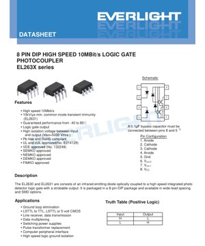
4.1 Pin Configuration and Schematic
The device is housed in a standard 8-pin Dual In-line Package (DIP).
- Pinout:
- Anode 1
- Cathode 1
- Cathode 2
- Anode 2
- Ground (GND)
- Output Voltage 2 (VOUT2)
- Output Voltage 1 (VOUT1)
- Supply Voltage (VCC)
- Truth Table (Positive Logic): Input HIGH = Output LOW; Input LOW = Output HIGH. The dual anode/cathode pins allow flexible connection of the input LED.
- Critical Bypassing: A 0.1 µF (or larger) ceramic capacitor with good high-frequency characteristics must be connected between VCC (pin 8) and GND (pin 5), placed as close as possible to the device pins. This is essential for stable operation and minimizing switching noise.
4.2 Soldering and Handling
The absolute maximum rating for soldering is 260°C for 10 seconds. This corresponds to a standard lead-free reflow profile. For wave or hand soldering, contact time and temperature should be controlled to prevent package damage. Standard ESD (Electrostatic Discharge) precautions should be observed during handling.
5. Application Guidelines and Design Considerations
5.1 Typical Application Circuits
EL263X ni versatile. Key applications ni:
- Digital Interface Isolation: Isolating UART, SPI, or I2C lines between a microcontroller and a peripheral in a different power domain or a noisy environment.
- Switching Power Supply Feedback: Isolating the feedback error signal from the secondary (output) side to the primary-side controller, providing safety isolation and noise immunity from power switching transients.
- Ground Loop Breaker in Data Lines: Preventing circulating currents and noise in communication links between systems with separate grounds.
- Logic Level Translator with Isolation: Shifting voltage levels (e.g., 3.3V to 5V) while also providing galvanic isolation.
5.2 Critical Design Considerations
- Input Current Setting: Choose IF based on speed and margin. The test condition is 7.5mA. Using 10-16 mA provides faster switching and better noise margin but increases power dissipation. Always use a series resistor: RIN = (VDRIVE - VF) / IF. Remember VF decreases with temperature.
- Output Load: The test load is 350Ω to VCC. The output can sink a minimum of 13mA (IOL condition) while maintaining VOL < 0.6V. Do not exceed the maximum output current (IO = 50 mA).
- Power Supply Decoupling: The 0.1 µF bypass capacitor is non-negotiable. Its absence can lead to oscillations, false triggering, or degraded CMTI performance.
- Layout for High CMTI: To achieve the rated CMTI, minimize parasitic capacitance across the isolation barrier. Keep input and output traces physically separated on the PCB. Follow the manufacturer's recommended creepage and clearance distances for the 5000Vrms isolation.
- Choosing EL2630 vs. EL2631: The primary difference is the guaranteed CMTI. Use the EL2631 in applications with extremely high dV/dt noise, such as in motor drives or high-power inverters. The EL2630 is suitable for less demanding environments.
6. Technical Comparison and Differentiation
Compared to standard 4N25/4N35 series photocouplers (which are transistor output), the EL263X offers decisive advantages for digital systems:
- Speed: 10 Mbit/s vs. typically < 100 kbit/s for transistor-output couplers.
- Output Type: Logic gate output with active pull-up and pull-down provides clean, fast edges and direct logic compatibility, unlike the open-collector transistor output which requires an external pull-up resistor and is slower.
- CMTI: Specified and guaranteed high CMTI (10 kV/µs) is a critical metric for industrial robustness, often not specified or much lower in basic couplers.
Compared to other high-speed couplers or digital isolators (based on capacitive or magnetic coupling), photocouplers like the EL263X offer the advantage of being based on well-understood optical technology with high intrinsic immunity to magnetic fields.
7. Frequently Asked Questions (Based on Parameters)
Q: What is the maximum data rate I can achieve?
A: The device is characterized for 10 Mbit/s operation. The limiting factors are the propagation delays and pulse width distortion. For a 50% duty cycle square wave, the maximum frequency is approximately 1/(2 * tPHL) or 1/(2 * tPLH), whichever is smaller. Using max delays (100 ns), this gives ~5 MHz. However, for non-return-to-zero (NRZ) data, the 10 Mbit/s rate is valid.
Q: Why is a bypass capacitor mandatory?
A: The high-speed switching of the internal output stage causes sudden current spikes on the VCC line. Without a local, low-inductance capacitor, these spikes can cause the internal supply voltage to droop or spike, leading to erratic operation, reduced noise margin, and failure to meet the CMTI specification.
Q: Can I drive the input directly from a microcontroller pin?
A> Yes, but you must tumia kipingamanishi cha kuzuia mkondo. Pini ya kawaida ya microcontroller kwenye 3.3V au 5V inaweza kutoa/kupokea mkondo wa kutosha. Kwa mfano, kupata IF ≈ 10mA kutoka kwa pini ya 3.3V: R = (3.3V - 1.4V) / 0.01A = 190Ω (tumia thamani ya kawaida ya 180Ω au 200Ω). Daima thibitisha uwezo wa mkondo wa pini ya MCU.
Q: What does the "strobable output" feature mean?
A: This refers to the ability to force the output into a high-impedance state. While the provided truth table doesn't show a disable function, some logic gate photocouplers have an output enable pin. The EL263X description mentions it, but the pinout and table do not show a dedicated pin for this. Designers should confirm this feature's implementation in the specific variant.
8. Practical Design Case Study
Scenario: Isolating a 1 Mbit/s UART signal between a 3.3V sensor node and a 5V system controller in an industrial setting with motor noise.
Design Steps:
- Part Selection: Choose EL2631 for its higher guaranteed CMTI (10 kV/µs) to withstand noise from nearby motors.
- Input Circuit: The TX pin of the 3.3V sensor drives the photocoupler input. Calculate series resistor for IF = 10mA: RIN = (3.3V - 1.4V) / 0.01A = 190Ω. Use a 180Ω resistor. Connect anode (pin 1 or 4) to the resistor, cathode (pin 2 or 3) to sensor GND.
- Output Circuit: Supply VCC = 5V from the controller side. Place a 0.1 µF ceramic capacitor directly between pin 8 (VCC) and pin 5 (GND). Connect the output pin (6 or 7) to the RX pin of the 5V controller. A series resistor (e.g., 100Ω) may be added to limit current if needed, but is not strictly required for logic input.
- PCB Layout: Place the photocoupler straddling the isolation gap on the PCB. Ensure >8mm creepage/clearance (consult safety standards for 5000Vrms) between all input-side and output-side copper pours, components, and traces. Keep the bypass capacitor leads very short.
- Verification: With this setup, a logic HIGH (3.3V) from the sensor TX will turn on the LED, causing the output to go LOW (<0.6V), which the 5V controller reads as a logic LOW. The signal is inverted, which can be corrected in software if necessary.
9. Operating Principle
The EL263X operates on the principle of optical coupling. An electrical input signal drives an infrared Light Emitting Diode (LED). When forward-biased, the LED emits infrared light. This light traverses a transparent isolation barrier (typically a molded plastic gap). On the other side, a monolithic silicon photodetector and integrated circuit detect this light. The IC includes a high-gain amplifier, a Schmitt trigger for noise immunity, and a totem-pole output driver stage. The driver actively pulls the output pin HIGH (towards VCC) or LOW (towards GND) based on the presence or absence of light, creating a clean, buffered logic signal that is electrically isolated from the input. The isolation barrier provides high voltage withstand capability and prevents ground loops.
10. Technology Trends
Photocoupler technology continues to evolve. Trends relevant to devices like the EL263X include:
- Higher Speeds: Maendeleo yanayoendelea yanalenga viwango vya data vinavyozidi 50 Mbit/s na hata kufikia safu ya 100+ Mbit/s kwa interfaces za kisasa za serial zenye kasi kubwa.
- Matumizi ya Nguvu ya Chini: Kupunguza mahitaji ya sasa ya LED ya ingizo (IF) and the output supply current (ICC) to meet the demands of portable and energy-efficient devices.
- Enhanced Integration: Combining multiple isolation channels (dual, quad) in a single package to save board space and cost in multi-line interfaces like SPI or isolated GPIO.
- Improved CMTI: As power electronics switching speeds increase (e.g., with SiC and GaN transistors), the demand for isolators with even higher CMTI ratings (25-100 kV/µs) grows to maintain reliability.
- Package Miniaturization: Moving from through-hole DIP packages to surface-mount options like SOIC-8 and even smaller wide-body SOIC packages to accommodate denser PCB designs.
The EL263X series sits in a well-established performance bracket, offering a robust balance of speed, isolation strength, and noise immunity for a wide range of industrial and communication applications.
LED Specification Terminology
Complete explanation of LED technical terms
Photoelectric Performance
| Term | Unit/Representation | Simple Explanation | Why Important |
|---|---|---|---|
| Luminous Efficacy | lm/W (lumens per watt) | Light output per watt of electricity, higher means more energy efficient. | Directly determines energy efficiency grade and electricity cost. |
| Luminous Flux | lm (lumens) | Total light emitted by source, commonly called "brightness". | Determines if the light is bright enough. |
| Viewing Angle | ° (degrees), e.g., 120° | Angle where light intensity drops to half, determines beam width. | Affects illumination range and uniformity. |
| CCT (Zazzabin Launi) | K (Kelvin), misali, 2700K/6500K | Gyalang/ngyilang na gyalang, gyalang na gyalang na gyalang, gyalang na gyalang na gyalang. | Gyalang na gyalang na gyalang na gyalang na gyalang. |
| CRI / Ra | Unitless, 0–100 | Ability to render object colors accurately, Ra≥80 is good. | Affects color authenticity, used in high-demand places like malls, museums. |
| SDCM | MacAdam ellipse steps, e.g., "5-step" | Color consistency metric, smaller steps mean more consistent color. | Ensures uniform color across same batch of LEDs. |
| Dominant Wavelength | nm (nanometers), e.g., 620nm (red) | Wavelength corresponding to color of colored LEDs. | Determines hue of red, yellow, green monochrome LEDs. |
| Spectral Distribution | Wavelength vs intensity curve | Shows intensity distribution across wavelengths. | Affects color rendering and quality. |
Electrical Parameters
| Term | Symbol | Simple Explanation | Design Considerations |
|---|---|---|---|
| Forward Voltage | Vf | Minimum voltage to turn on LED, like "starting threshold". | Driver voltage must be ≥Vf, voltages add up for series LEDs. |
| Forward Current | If | Current value for normal LED operation. | Usually constant current drive, current determines brightness & lifespan. |
| Max Pulse Current | Ifp | Peak current tolerable for short periods, used for dimming or flashing. | Pulse width & duty cycle must be strictly controlled to avoid damage. |
| Reverse Voltage | Vr | Max reverse voltage LED can withstand, beyond may cause breakdown. | Circuit must prevent reverse connection or voltage spikes. |
| Thermal Resistance | Rth (°C/W) | Resistance to heat transfer from chip to solder, lower is better. | High thermal resistance requires stronger heat dissipation. |
| ESD Immunity | V (HBM), e.g., 1000V | Ability to withstand electrostatic discharge, higher means less vulnerable. | Anti-static measures needed in production, especially for sensitive LEDs. |
Thermal Management & Reliability
| Term | Key Metric | Simple Explanation | Impact |
|---|---|---|---|
| Junction Temperature | Tj (°C) | Halin zazzabi na aiki a cikin LED chip. | Kowane raguwar 10°C na iya ninka tsawon rayuwa; yana da yawa yana haifar da lalacewar haske, canjin launi. |
| Lumen Depreciation | L70 / L80 (hours) | Time for brightness to drop to 70% or 80% of initial. | Directly defines LED "service life". |
| Lumen Maintenance | % (e.g., 70%) | Percentage of brightness retained after time. | Indicates brightness retention over long-term use. |
| Color Shift | Δu′v′ or MacAdam ellipse | Degree of color change during use. | O nifẹ si iṣọkan awọ ninu awọn ayẹyẹ itansan. |
| Thermal Aging | Material degradation | Deterioration due to long-term high temperature. | May cause brightness drop, color change, or open-circuit failure. |
Packaging & Materials
| Term | Common Types | Simple Explanation | Features & Applications |
|---|---|---|---|
| Package Type | EMC, PPA, Ceramic | Housing material protecting chip, providing optical/thermal interface. | EMC: good heat resistance, low cost; Ceramic: better heat dissipation, longer life. |
| Chip Structure | Front, Flip Chip | Chip electrode arrangement. | Flip chip: better heat dissipation, higher efficacy, for high-power. |
| Phosphor Coating | YAG, Silicate, Nitride | Covers blue chip, converts some to yellow/red, mixes to white. | Different phosphors affect efficacy, CCT, and CRI. |
| Lens/Optics | Flat, Microlens, TIR | Optical structure on surface controlling light distribution. | Determines viewing angle and light distribution curve. |
Quality Control & Binning
| Term | Binning Content | Simple Explanation | Purpose |
|---|---|---|---|
| Luminous Flux Bin | Code e.g., 2G, 2H | Grouped by brightness, each group has min/max lumen values. | Ensures uniform brightness in same batch. |
| Voltage Bin | Code e.g., 6W, 6X | Grouped by forward voltage range. | Facilitates driver matching, improves system efficiency. |
| Color Bin | 5-step MacAdam ellipse | Grouped by color coordinates, ensuring tight range. | Guarantees color consistency, avoids uneven color within fixture. |
| CCT Bin | 2700K, 3000K etc. | Grouped by CCT, each has corresponding coordinate range. | Meets different scene CCT requirements. |
Testing & Certification
| Term | Standard/Test | Simple Explanation | Significance |
|---|---|---|---|
| LM-80 | Lumen maintenance test | Long-term lighting at constant temperature, recording brightness decay. | Used to estimate LED life (with TM-21). |
| TM-21 | Life estimation standard | Estimates life under actual conditions based on LM-80 data. | Provides scientific life prediction. |
| IESNA | Illuminating Engineering Society | Covers optical, electrical, thermal test methods. | Industry-recognized test basis. |
| RoHS / REACH | Environmental certification | Ensures no harmful substances (lead, mercury). | Market access requirement internationally. |
| ENERGY STAR / DLC | Energy efficiency certification | Energy efficiency and performance certification for lighting. | Used in government procurement, subsidy programs, enhances competitiveness. |