Table of Contents
- 1. Product Overview
- 1.1 Core Advantages and Target Market
- 2. In-depth Technical Parameter Analysis
- 2.1 Absolute Maximum Ratings
- 2.2 Electro-Optical Characteristics
- 2.2.1 Input Characteristics (LED Side)
- 2.2.2 Output Characteristics (Phototransistor Side)
- 2.2.3 Transfer Characteristics
- 3. Performance Curve Analysis
- 4. Mechanical and Packaging Information
- 4.1 Package Dimensions and Options
- 4.2 Polarity Identification and Marking
- 4.3 Recommended Pad Layout
- 5. Soldering and Assembly Guide
- 6. Packaging and Ordering Information
- 6.1 Model Numbering Rule
- 6.2 Tape and Reel Specification
- 7. Application Notes and Design Considerations
- 7.1 Typical Application Circuit
- 7.2 Key Design Factors
- 8. Technical Comparison and Differentiation
- 9. Frequently Asked Questions (Based on Technical Parameters)
- A: Use through-hole DIP packages for applications such as prototyping, manual assembly, or where board space is not a major concern and the mechanical strength of pin-through-hole soldering is desired. Choose SMD (S1) packages for automated assembly, high-density PCB design, and requirements to reduce board thickness.
- This simple circuit provides robust isolated digital signal transmission.
- ). The ratio of this output collector current to the input LED current is the Current Transfer Ratio (CTR). There is no electrical connection between the input and output circuits; only light couples them, thereby providing electrical isolation.
- Detailed Explanation of LED Specification Terminology
- I. Core Photometric and Electrical Performance Indicators
- II. Electrical Parameters
- III. Thermal Management and Reliability
- IV. Packaging and Materials
- V. Quality Control and Binning
- VI. Testing and Certification
1. Product Overview
Jerin EL851 yana wakiltar nau'in hadaddiyar haske mai ƙarfi na transistor na haske wanda aka tsara don keɓewar lantarki mai ƙarfi a cikin aikace-aikace masu tsauri. Waɗannan na'urorin sun haɗa diode mai fitar da infrared wanda aka haɗa shi da na'urar gano transistor na haske na silicon, kuma an haɗa su a cikin ƙaramin fakitin shigar da layi biyu (DIP) mai ƙafafu 4. Babban aikinsa shine watsa siginar lantarki tsakanin da'irori biyu masu keɓewa ta amfani da haske, don haka hana babban ƙarfin lantarki ko amo daga gefen fitarwa ya yadu zuwa gefen shigarwa, ko akasin haka. Wannan jerin yana da alaƙa da babban ƙimar ƙarfin lantarki na mai tarawa-mai fitarwa, wanda ya sa ya dace don haɗawa da da'irorin wutar lantarki da sauran tsarin babban ƙarfin lantarki.
1.1 Core Advantages and Target Market
Jerin EL851 yana ba da fa'idodi masu mahimmanci da yawa waɗanda suka tabbatar da matsayinsa a kasuwa. Fitaccen sifarsa shine babban ƙimarVCEO350V, wanda ke ba shi damar jurewa babban bambanci na ƙarfin lantarki tsakanin gefen shigarwa da na fitarwa. Wannan yana tare da babban ƙimarVISO5000 VrmsHigh isolation voltage ( ), ensuring a reliable safety barrier in industrial and telecommunications equipment. These devices comply with major international safety standards including UL, cUL, VDE, and various other regional certifications (SEMKO, NEMKO, DEMKO, FIMKO, CQC), facilitating their entry into the global market. Furthermore, the series is designed to be halogen-free (for copper lead frame versions) and complies with RoHS and EU REACH regulations, meeting modern environmental and regulatory requirements. Target applications include telephone line interfaces, power circuit interfaces, solid-state relays (SSR) and DC motor controllers, as well as programmable controllers where signal isolation and noise immunity are critical.
2. In-depth Technical Parameter Analysis
A thorough understanding of the device's electrical and optical characteristics is crucial for proper circuit design and reliable operation.
2.1 Absolute Maximum Ratings
Absolute Maximum Ratings define the stress limits that may cause permanent damage to the device. These values are not intended for normal operating conditions. Key ratings for the EL851 include:
- Input Forward Current (IF)): 60 mA (continuous).
- Peak forward current (IFM)): 1 A (for a 1µs pulse), suitable for brief surge conditions.
- Collector-emitter voltage (VCEO)): 350 V, this is the maximum voltage that can be applied across the output transistor when the base is open.
- Collector current (IC)): 50 mA.
- Total power dissipation (PTOT)): 200 mW, combines input and output power limitations.
- Isolation voltage (VISO)): 5000 Vrms(for 1 minute at 40-60% relative humidity). This test is conducted with pins 1 and 2 shorted, and pins 3 and 4 shorted.
- Operating temperature (TOPR)): -55°C to +100°C.
- Soldering temperature (TSOL)): 260°C for 10 seconds, applicable to wave soldering or reflow soldering processes.
2.2 Electro-Optical Characteristics
These parameters are typically specified at 25°C, describing the device's performance under normal operating conditions.
2.2.1 Input Characteristics (LED Side)
- Forward Voltage (VF)): Typical value 1.2V, maximum 1.4V at IF= 10 mA. This is used to calculate the required current-limiting resistor on the input side.
- Reverse Current (IR)): At VRMaximum 10 µA at = 5V, indicating very low leakage current when the LED is reverse biased.
- Input capacitance (Cin)): Typical value 30 pF, maximum 250 pF. This may affect high-frequency switching performance on the input side.
2.2.2 Output Characteristics (Phototransistor Side)
- Collector-emitter dark current (ICEO)): At VCEMaximum 100 nA at = 200V. This is the leakage current when the LED is off (no light), crucial for determining "off-state" signal integrity.
- Collector-emitter breakdown voltage (BVCEO)): In IC= 0.1mA, the minimum is 350V, confirming its high-voltage capability.
- Collector-emitter capacitance (CCE)): At VCE= 0V, the typical value is 10 pF.
2.2.3 Transfer Characteristics
- Current Transfer Ratio (CTR)): In IF= 5mA and VCE= 5V, the range is from 50% to 600%. CTR is defined as (IC/ IF) * 100%. A higher CTR allows a given output current to be driven with a lower input current, thereby improving efficiency. A wide range indicates the existence of a binning system; designers must consider the minimum CTR in the circuit to ensure proper functionality.
- Collector-Emitter Saturation Voltage (VCE(sat))): In IF= 20mA and IC= 0.4V maximum at 1mA. This low saturation voltage is very important when the phototransistor is used as a switch in the "on" state, minimizing voltage drop and power loss.
- Isolation Resistance (RIO)): At V11= 500V DC minimum 10IOΩ, yana nuna cewa akwai keɓancewar DC mai kyau tsakanin shigarwa da fitarwa.
- Ƙarfin ƙarfin shigarwa-fitarwa (CIO)): Matsakaicin ƙima 0.6 pF, ƙasa sosai, yana taimakawa wajen rage mafi ƙarancin haɗin ƙarfin ƙarfi ta hanyar shinge na keɓewa.
- Lokacin tashi (tr) da lokacin faɗuwa (tf)): Matsakaicin ƙimomi bi da bi 4 µs da 5 µs, a cikin yanayin gwaji (VCE=2V, IC=2mA, RL=100Ω) matsakaicin kowane 18 µs. Waɗannan sigogi suna bayyana saurin sauyawa na mai haɗin haske, yana da mahimmanci ga watsa siginar dijital ko aikace-aikacen PWM.
3. Performance Curve Analysis
Although specific graphical data is referenced in the PDF (typical optoelectronic characteristic curves, Figure 9), the key interpretation is based on the provided tabular data and test circuit.
The switching time test circuit shows a standard configuration where a pulsed current drives the input LED, and the response of the output phototransistor is measured across a load resistor (RL). The rise time (tr) is the time required for the output current to rise from 10% to 90% of its final value when the LED is turned on. The fall time (tf) is the time required to fall from 90% to 10% when the LED is turned off. Typical values in the 4-5 µs range indicate the device is suitable for medium-speed switching applications, such as relay driving or lower-frequency data line isolation, but may not be suitable for very high-speed digital communication.
4. Mechanical and Packaging Information
4.1 Package Dimensions and Options
The EL851 offers three main lead form options, each with specific dimensions and applications.
- Standard DIP type: The default through-hole package.
- M type option: Features wide pin bends with a pin pitch of 0.4 inches (approximately 10.16mm), suitable for circuit boards requiring wider pin spacing.
- S1 type option: A low-profile surface-mount (SMD) pin form. This is the SMD variant of the device.
Although precise numerical dimensions are provided in the PDF drawings, the overall package size of the standard DIP type is approximately 6.35mm in length, 4.57mm in width, and 3.3mm in height, making it a compact component.
4.2 Polarity Identification and Marking
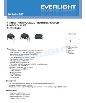
Pin configuration is standardized:
- Anode (Input LED Positive)
- Cathode (Input LED Negative)
- Emitter (Phototransistor Emitter, typically connected to ground/common on the output side)
- Collector (Phototransistor Collector, Output)
The top of the device is marked with "EL" (indicating the manufacturer), "851" (device number), followed by a one-digit year code (Y), a two-digit week code (WW), and an optional "V" indicating the VDE certified version. Correct identification of Pin 1 (typically indicated on the package by a dot, notch, or bevel) is crucial for proper orientation during assembly.
4.3 Recommended Pad Layout
For the S1 (surface mount) option, a recommended land pattern is provided. The suggested dimensions are for reference only; designers are advised to modify them based on their specific PCB fabrication process, solder paste application, and thermal management requirements to ensure reliable solder joints.
5. Soldering and Assembly Guide
This device can withstand soldering temperatures up to 260°C for a maximum of 10 seconds. This is compatible with standard wave soldering for through-hole packages and lead-free reflow profiles for SMD options. Strict adherence to this time-temperature limit is critical to prevent damage to the internal die, bond wires, or plastic package material. Standard ESD (Electrostatic Discharge) precautions should be observed during handling and assembly. The storage temperature range is -55°C to +125°C.
6. Packaging and Ordering Information
6.1 Model Numbering Rule
Part numbers follow the format:EL851X(Z)-V.
- X: Pin form option.
- None: Standard DIP-4 (100 pieces/tube).
- M: Wide pin bend, 0.4" pitch (100 pieces/tube).
- S1: Surface mount pin form (low profile).
- Z: Tape and reel packaging option (for S1 only).
- TA, TB, TU, TD: Different reel specifications affecting packaging quantity (1000 or 1500 pieces per reel).
- V: Optional suffix indicating VDE safety certification.
6.2 Tape and Reel Specification
Provides detailed reel dimensions (A, B, D0, D1, E, F, P0, P1, P2, t, W, K) for the S1 option. These dimensions are crucial for PCB assembly machines to correctly pick and place components from the reel. The reel width (W) is 16.0mm ±0.3mm, and the pocket pitch (P0) is 4.0mm ±0.1mm.
7. Application Notes and Design Considerations
7.1 Typical Application Circuit
The EL851 is ideally suited for the following key applications:
- Mahadar layin tarho: Keɓance sassan dabaru masu hankali na modem ko tsarin tarho daga babban siginar ƙararrawa da ƙarar ruwa mai yuwuwa akan layin tarho.
- Madauki da mayar da martani na wutar lantarki: Samar da keɓantaccen mayar da martani na fitarwar ƙarfin lantarki a cikin mai canza wutar lantarki (SMPS), yana tabbatar da daidaitaccen ƙarfin lantarki yayin kiyaye tsaro tsakanin ɓangaren farko (babban ƙarfi) da na biyu (ƙaramin ƙarfi).
- SSR da sarrafa injin DC: Gudanar da ƙofar ko shigarwar SSR, ko a matsayin keɓantaccen mahada tsakanin microcontroller da gadar H mai sarrafa injin, yana kare mai sarrafa dabaru daga hayaniyar injin da ƙararrakin ƙarfin lantarki.
- Module na Shigarwa/Fitarwa na Mai Sarrafa Na'ura Mai Kwakwalwa (PLC)Isolate digital input/output channels to protect the central processing unit from field wiring faults, noise, and different ground potentials.
7.2 Key Design Factors
- CTR DegradationThe CTR of an optocoupler degrades over time, especially when operating at high temperatures and high LED currents. For long-term reliability, the circuit should be designed to function properly even after accounting for an appropriate degradation margin (typically 50% over the product's lifetime).MinimumEnsure the specified CTR operates correctly.
- Input Current LimitationAn external resistor must always be connected in series with the input LED to limit the forward current (IF) is limited to a safe value, typically well below the absolute maximum of 60mA. The resistor value is calculated as Rlimit= (Vsupply- VF) / IF.
- Output load resistor: The value of the load resistor (RL) connected to the phototransistor collector affects the output voltage swing and switching speed. A smaller RLYana ba da damar gudun mafi girma, amma zai rage ribar fitar da wutar lantarki. RL=100Ω yanayin gwaji yana ba da ma'anar lokacin sauyawa da aka kayyade.
- Ƙarfin jure hayaniyar: Ko da yake na'urar tana ba da keɓancewar lantarki mai kyau, amma ƙaramin ƙaramin ƙarfin shigarwa-fitowa (0.6 pF) yana taimakawa wajen rage haɗin hayaniyar mita mai girma. Don yanayi masu tsananin hayaniya, yana iya buƙatar ƙarin tacewa akan siginar shigarwa da fitarwa.
- Haskakawa: Tabbatar da jimlar amfani da wutar lantarki (PTOT= VF*IF+ VCE*IC) Not exceeding 200 mW, while considering the maximum operating ambient temperature. Derating may be necessary at temperatures above 25°C.
8. Technical Comparison and Differentiation
Compared to standard low-voltage optocouplers (typically VCEOratings of 30-70V), the 350V rating of the EL851 is its primary differentiating feature. This allows it to be used directly in offline power supply feedback circuits (where the rectified mains voltage can be around 300V+) or industrial control interfaces without requiring additional voltage clamping or step-down circuits on the output side. Its wide CTR range provides options for both sensitive and standard driving requirements. It is offered in both through-hole (DIP, wide bend) and surface-mount (S1) tape and reel packaging, making it suitable for prototyping as well as high-volume automated assembly, offering broad applicability.
9. Frequently Asked Questions (Based on Technical Parameters)
- Q: What minimum CTR should I design for?
- A: Always design for the minimum CTR you expect at your operating IFand VCEDesign your circuit based on a minimum CTR of 50% under the specified conditions. Also consider potential degradation over the product's lifetime.
- Q: Can I use this optocoupler to directly switch a 120VAC load?
- A: No. VCEOrating is 350V DC. The peak voltage of 120VAC is approximately 170V, which is within the rating. However, the optocoupler's phototransistor is not designed to handle the high current of an AC load directly. It should be used to drive the control input of a separate high-power switch (such as a TRIAC, MOSFET, or SSR).
- Q: VCEOand VISO?
- What is the difference?CEOAmsa: VISO(350V) shine ne da mafi girman ƙarfin lantarki na DC da za a iya amfani da shi tsakanin tashar taro da fitar da fitilun transistor. V(5000 Vrms
- ) shine gwajin ƙarfin lantarki na AC da aka gwada tsakanin gajerun hanyoyin shigarwa (1,2) da gajerun hanyoyin fitarwa (3,4), wanda ke wakiltar ƙarfin keɓancewar shinge na filastik na ciki.
- Tambaya: Yaya ake zaɓar tsakanin DIP da SMD encapsulation?
A: Use through-hole DIP packages for applications such as prototyping, manual assembly, or where board space is not a major concern and the mechanical strength of pin-through-hole soldering is desired. Choose SMD (S1) packages for automated assembly, high-density PCB design, and requirements to reduce board thickness.
10. Practical Design Example
Scenario: Isolated digital input for 24V industrial sensors.Objective:
Connect a 24V proximity sensor to a 3.3V microcontroller, providing isolation to protect the MCU from voltage transients on the 24V line.
- Circuit Design:Input Side:The sensor output (sinking type) is connected between +24V and the anode (Pin 1) of the EL851. A current-limiting resistor (Rin) is placed between the cathode (pin 2) and ground. When the sensor is active, select RinFto set IFto a nominal 5-10 mA. For example, assuming V~1.2V, then Rin
- = (24V - 1.2V) / 0.005A ≈ 4.56kΩ (use the standard 4.7kΩ value).Output side:The phototransistor collector (pin 4) is connected through a pull-up resistor (Rpullup). The emitter (pin 3) is connected to MCU ground. When the sensor is activated, the LED illuminates, the phototransistor saturates, pulling the collector (output signal) low (approx. 0.4V). When the sensor is off, the phototransistor is off, Rpulluppulls the output high to 3.3V. Select Rpullup
- based on the required speed and power consumption; 1kΩ to 10kΩ are common values.Isolation:The 24V sensor ground and the 3.3V MCU ground are completely separate. The EL851's 5000Vrms
This simple circuit provides robust isolated digital signal transmission.
11. Operating PrincipleFEThe EL851 operates based on the principle of optoelectronic conversion and isolation. The current applied to the input side flows through an infrared light-emitting diode (LED), causing it to emit light. This light passes through a transparent isolation gap within the plastic package and strikes the base region of a silicon phototransistor on the output side. The incident light generates electron-hole pairs in the base region, effectively acting as a base current. This photogenerated base current is amplified by the transistor's current gain (hC), producing a larger collector current (I
). The ratio of this output collector current to the input LED current is the Current Transfer Ratio (CTR). There is no electrical connection between the input and output circuits; only light couples them, thereby providing electrical isolation.
12. Technology Trends
Detailed Explanation of LED Specification Terminology
Complete Explanation of LED Technical Terminology
I. Core Photometric and Electrical Performance Indicators
| Terminology | Unit/Representation | Layman's Explanation | Why It Is Important |
|---|---|---|---|
| Luminous Efficacy | lm/W | The luminous flux emitted per watt of electrical power; higher values indicate greater energy efficiency. | Directly determines the energy efficiency rating of the luminaire and the electricity cost. |
| Luminous Flux | lm | Total light output from a light source, commonly known as "brightness". | Determines if a luminaire is bright enough. |
| Viewing Angle | ° (degree), e.g., 120° | The angle at which light intensity drops to half, determining the beam width. | Affects the illumination range and uniformity. |
| Yanayin zafi na launi (CCT) | K (Kelvin), misali 2700K/6500K | Yanayin zafi na haske, ƙananan ƙima ja/ dumi, babban ƙima fari/ sanyi. | Yana ƙayyade yanayin haske da yanayin da ya dace. |
| Ma'aunin nuna launi (CRI / Ra) | Babu raka'a, 0–100 | The ability of a light source to reproduce the true colors of objects, Ra≥80 is preferred. | Affects color fidelity, used in high-demand places such as shopping malls and art galleries. |
| Chromaticity Tolerance (SDCM) | MacAdam ellipse steps, e.g., "5-step" | A quantitative indicator of color consistency; the smaller the step number, the more consistent the color. | Ensures no color variation among the same batch of luminaires. |
| Dominant Wavelength | nm (nanometer), e.g., 620nm (red) | The wavelength value corresponding to the color of a colored LED. | Determines the hue of monochromatic LEDs such as red, yellow, and green. |
| Spectral Distribution | Wavelength vs. Intensity curve | It shows the intensity distribution of light emitted by the LED at various wavelengths. | Affects color rendering and color quality. |
II. Electrical Parameters
| Terminology | Symbol | Layman's Explanation | Design Considerations |
|---|---|---|---|
| Forward Voltage | Vf | Voltage ya chini inayohitajika kuwasha LED, kama "kizingiti cha kuanzisha". | Voltage ya chanzo cha umeme inahitaji kuwa ≥ Vf, voltage inajumlishwa wakati LED nyingi zimeunganishwa mfululizo. |
| Mkondo wa Mbele (Forward Current) | If | Thamani ya mkondo inayofanya LED ionyeshe mwanga kwa kawaida. | Constant current drive is often used, as the current determines brightness and lifespan. |
| Maximum Pulse Current (Pulse Current) | Ifp | The peak current that can be withstood in a short time, used for dimming or flashing. | Pulse width and duty cycle must be strictly controlled, otherwise overheating damage will occur. |
| Reverse Voltage (Reverse Voltage) | Vr | The maximum reverse voltage that an LED can withstand; exceeding this may cause breakdown. | The circuit must be protected against reverse connection or voltage surges. |
| Thermal Resistance | Rth (°C/W) | The resistance to heat flow from the chip to the solder point; a lower value indicates better heat dissipation. | High thermal resistance requires a stronger heat dissipation design; otherwise, the junction temperature will increase. |
| Electrostatic Discharge Immunity (ESD Immunity) | V (HBM), e.g., 1000V | The ability to withstand electrostatic discharge; a higher value indicates greater resistance to damage from static electricity. | Anti-static measures must be implemented during production, especially for high-sensitivity LEDs. |
III. Thermal Management and Reliability
| Terminology | Maɗaukakin Ma'auni | Layman's Explanation | Tasiri |
|---|---|---|---|
| Junction Temperature | Tj(°C) | Ainihin yanayin zafi a cikin guntu na LED. | Kowane raguwa na 10°C, rayuwa na iya tsawaita sau biyu; yawan zafi yana haifar da raguwar haske, karkatar launi. |
| Lumen Depreciation | L70 / L80 (hours) | The time required for brightness to drop to 70% or 80% of its initial value. | Directly defines the "useful life" of an LED. |
| Lumen Maintenance | % (e.g., 70%) | The percentage of remaining brightness after a period of use. | Characterizes the ability to maintain brightness after long-term use. |
| Color Shift | Δu′v′ or MacAdam Ellipse | The degree of color change during use. | Affects the color consistency of a lighting scene. |
| Thermal Aging | Decline in material performance. | Degradation of packaging materials due to prolonged high temperatures. | May lead to decreased brightness, color change, or open-circuit failure. |
IV. Packaging and Materials
| Terminology | Common Types | Layman's Explanation | Characteristics and Applications |
|---|---|---|---|
| Package Types | EMC, PPA, Ceramic | The housing material that protects the chip and provides optical and thermal interfaces. | EMC offers good heat resistance and low cost; ceramic provides superior heat dissipation and long lifespan. |
| Chip Structure | Front-side, Flip Chip | Chip Electrode Layout. | Flip Chip offers better heat dissipation and higher luminous efficacy, suitable for high-power applications. |
| Phosphor Coating | YAG, Silicate, Nitride | Coated on the blue LED chip, partially converts to yellow/red light, mixing to form white light. | Different phosphors affect luminous efficacy, color temperature, and color rendering. |
| Lens/Optical Design | Flat, microlens, total internal reflection | Optical structure on the package surface, controlling light distribution. | Determines the beam angle and light distribution curve. |
V. Quality Control and Binning
| Terminology | Grading Content | Layman's Explanation | Purpose |
|---|---|---|---|
| Luminous Flux Grading | Codes such as 2G, 2H | Grouped by brightness level, each group has a minimum/maximum lumen value. | Ensure consistent brightness within the same batch of products. |
| Voltage Binning | Codes such as 6W, 6X | Group according to forward voltage range. | Facilitates driver matching and improves system efficiency. |
| Chromaticity Binning | 5-step MacAdam ellipse | Group by color coordinates to ensure colors fall within an extremely narrow range. | Ensure color consistency to avoid color variation within the same luminaire. |
| Color temperature binning | 2700K, 3000K, etc. | Group by color temperature, each group has a corresponding coordinate range. | Meet the color temperature requirements for different scenarios. |
VI. Testing and Certification
| Terminology | Standard/Test | Layman's Explanation | Significance |
|---|---|---|---|
| LM-80 | Lumen Maintenance Test | Long-term operation under constant temperature conditions, recording brightness attenuation data. | Used to estimate LED lifetime (combined with TM-21). |
| TM-21 | Lifetime extrapolation standard | Estimate lifetime under actual use conditions based on LM-80 data. | Provide scientific lifetime prediction. |
| IESNA standard | Illuminating Engineering Society Standard | Covers optical, electrical, and thermal test methods. | Industry-recognized testing basis. |
| RoHS / REACH | Environmental Certification | Ensures products are free from harmful substances (e.g., lead, mercury). | Market access requirements for entering international markets. |
| ENERGY STAR / DLC | Energy efficiency certification. | Energy efficiency and performance certification for lighting products. | Commonly used in government procurement and subsidy programs to enhance market competitiveness. |