Table of Contents
- 1. Product Overview
- 1.1 Core Advantages and Target Market
- 2. In-depth Technical Parameter Analysis
- 2.1 Absolute Maximum Ratings
- 2.2 Electro-Optical Characteristics (Ta=25°C)
- 3. Performance Curve Analysis
- 3.1 Forward Current vs. Ambient Temperature
- 3.2 Spectral Distribution
- 3.3 Relationship Between Peak Emission Wavelength and Ambient Temperature
- 3.4 Relationship between Forward Voltage and Ambient Temperature
- 3.5 Relative Radiation Intensity vs. Angular Displacement
- 4. Mechanical and Packaging Information
- 4.1 Package Dimensions (0603)
- 4.2 Polarity Marking
- 4.3 Tape and Reel Specifications
- 5. Welding and Assembly Guide
- 5.1 Moisture Sensitivity and Storage
- 5.2 Reflow Soldering Temperature Profile
- 5.3 Manual Soldering and Rework
- 6. Application Design Considerations
- 6.1 Dole ne dole a yi amfani da matakan iyakancewar kwarara.
- 6.2 Gudanar da zafi.
- 6.3 Optical Design
- 6.4 Circuit Protection
- 7. Comparison and Selection Guide
- 8. Frequently Asked Questions (Based on Technical Specifications)
- 8.1 What is the 870nm wavelength used for?
- 8.2 Shin za a iya kunna wannan LED kai tsaye ta hanyar microcontroller pin na 3.3V ko 5V?
- 8.3 Yaya zafin jiki ke tasiri aikin?
- 8.4 Is a heat sink necessary?
- 9. Practical Application Example: Simple Infrared Proximity Sensor
- 10. Working Principle and Technology Trends
- 10.1 Basic Working Principles
- 10.2 Industry Trends
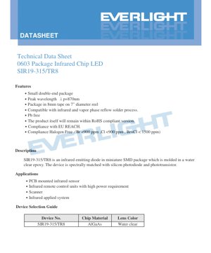
1. Product Overview
This document details the specifications of a high-performance miniature surface-mount infrared emitting diode. The device employs a compact 0603 package, making it suitable for applications with space constraints that require reliable infrared emission. Its primary function is to emit light in the near-infrared spectrum, with a typical peak wavelength of 870 nanometers, achieving optimal spectral matching with silicon photodiodes and phototransistors. The core material is AlGaAs (aluminum gallium arsenide), renowned for its efficient infrared light generation capability.
1.1 Core Advantages and Target Market
该器件为现代电子设计提供了多项关键优势。其微型双端SMD封装支持高密度PCB贴装,并与自动化贴片组装工艺兼容。它设计为兼容红外和汽相回流焊接,便于现代制造流程。该产品符合主要的环境和安全标准,包括RoHS(有害物质限制)、欧盟REACH法规,并且不含卤素(Br <900 ppm, Cl <900 ppm, Br+Cl < 1500 ppm)。这种小尺寸、高性能与合规性的结合,使其成为消费电子、工业传感器和通信设备的理想选择。
Main applications include:
- PCB-mounted infrared proximity and presence sensors.
- Infrared remote control unit with higher radiant intensity is required.
- Barcode scanners and optical encoders.
- Various infrared-based data transmission and sensing systems.
2. In-depth Technical Parameter Analysis
A thorough understanding of electrical and optical parameters is crucial for reliable circuit design and ensuring the LED operates within its safe operating area.
2.1 Absolute Maximum Ratings
These ratings define the limits beyond which permanent damage to the device may occur. They are not intended for normal operation.
- Continuous Forward Current (IF):65 mA. Exceeding this current, even momentarily, may lead to catastrophic failure due to semiconductor junction overheating.
- Reverse Voltage (VR):5 V. This LED has a relatively low reverse breakdown voltage. Circuit design must ensure that the reverse bias voltage applied to the LED does not exceed this value; protective measures are often required in AC or bidirectional signal environments.
- Power Dissipation (Pc):110 mW at 25°C. This is the maximum power that the package can dissipate in the form of heat. The actual allowable power decreases as the ambient temperature (Ta) increases. High-temperature applications require derating.
- Temperature range:Operating temperature: -25°C to +85°C; Storage temperature: -40°C to +100°C.
- Welding Temperature (Tsol):260°C, maximum 5 seconds. This defines the reflow soldering temperature profile limits.
2.2 Photoelectric Characteristics (Ta=25°C)
These are typical performance parameters under specified test conditions. Designers should use typical or maximum/minimum values as appropriate based on their design margins.
- Radiation intensity (IE):At IFAt =20mA, the typical value is 1.3 mW/sr. Radiant intensity measures the light power emitted per unit solid angle (steradian). It is a key parameter for determining the signal strength at the receiver. The specified minimum value is 1.0 mW/sr.
- Peak Wavelength (λp):The typical value is 870 nm, ranging from 860 nm to 900 nm. This is the wavelength at which the emission spectrum is strongest. Matching this wavelength to the peak sensitivity of the receiver (e.g., a silicon photodetector with peak sensitivity around ~850-950nm) maximizes system efficiency.
- Spectral Bandwidth (Δλ):The typical value is 45 nm. This is the full width at half maximum of the emission spectrum, indicating the wavelength range of emission.
- Forward voltage (VF):At IF=20mA, the typical value is 1.35 V, ranging from 1.20 V to 1.70 V. This parameter is crucial for calculating the current-limiting resistor value: R = (Vsupply- VF) / IF. Its variation must be considered in robust design.
- Reverse current (IR):At VRAt =5V, the maximum value is 10 µA.
- Viewing Angle (2θ1/2):140 degrees. This is the full angle at which the radiation intensity drops to half of its peak (on-axis) value. A wide viewing angle is highly beneficial for applications requiring extensive coverage, such as proximity sensors.
3. Performance Curve Analysis
The provided characteristic curves offer valuable insights into the device's behavior under various conditions, which is crucial for practical application design.
3.1 Forward Current vs. Ambient Temperature
This curve illustrates the relationship between the maximum allowable continuous forward current and the ambient temperature. It indicates that as the temperature increases, it is necessary to derate the forward current to remain within the power dissipation limits. Near the maximum operating temperature (+85°C), the allowable continuous current is significantly lower than the 65mA absolute maximum rating at 25°C.
3.2 Spectral Distribution
Spectral distribution graph shows the variation of relative radiant power output with wavelength. It confirms the peak wavelength (λp) is 870nm, and the typical spectral bandwidth (Δλ) is approximately 45nm. The shape of this curve is crucial for filtering and ensuring compatibility with the receiver's spectral response.
3.3 Relationship Between Peak Emission Wavelength and Ambient Temperature
This curve shows that the peak wavelength has a positive temperature coefficient, meaning it slightly increases as the junction temperature rises. This shift (typically around 0.1-0.3 nm/°C for AlGaAs devices) is significant for precision sensing applications where wavelength stability is critical.
3.4 Relationship between Forward Voltage and Ambient Temperature
Forward voltage (VF) has a negative temperature coefficient; it decreases as temperature rises. This characteristic must be considered in constant-current drive circuits, as the lower VFIt may slightly affect power consumption calculations.
3.5 Relative Radiation Intensity vs. Angular Displacement
This polar plot visually defines the viewing angle (140° at the half-intensity points). For this package style, the radiation pattern is typically Lambertian or near-Lambertian, which is useful for simulating the irradiance on a target surface at various angles and distances.
4. Mechanical and Packaging Information
4.1 Package Dimensions (0603)
This device conforms to the standard 0603 (1608 metric) package dimensions: approximately 1.6mm in length, 0.8mm in width, and 0.8mm in height. The detailed dimension drawing specifies the pad layout, component outline, and terminal positions, with a standard tolerance of ±0.1mm unless otherwise noted. Proper pad pattern design is crucial for reliable soldering and mechanical stability.
4.2 Polarity Marking
The datasheet includes diagrams indicating the anode and cathode terminals. Correct polarity is essential for device operation. Typically, the cathode may be identified by a notch, a green indicator mark, or a specific pad shape on the tape and reel packaging.
4.3 Tape and Reel Specifications
The product is supplied in 8mm wide embossed carrier tape, wound on 7-inch diameter reels. The carrier tape dimensions are clearly specified to ensure compatibility with standard SMD assembly equipment. Each reel contains 4000 pieces.
5. Welding and Assembly Guide
Proper operation is crucial for maintaining device reliability and performance.
5.1 Moisture Sensitivity and Storage
This device is moisture-sensitive. Precautions include:
- Do not open the moisture barrier bag before use.
- Store unopened bags at ≤30°C and ≤90% RH.
- Use within one year after shipment.
- After opening, store at ≤30°C and ≤60% RH.
- Use within 168 hours (7 days) after opening the bag.
- If the storage time is exceeded or the desiccant indicates moisture ingress, bake at 60 ±5°C for at least 24 hours before use.
5.2 Reflow Soldering Temperature Profile
It is recommended to use a lead-free reflow soldering temperature profile. Key parameters include a peak temperature of 260°C, and the time above 240°C must not exceed the recommended limit (implied by a maximum of 5 seconds at 260°C). Reflow soldering should not be performed more than twice to avoid excessive thermal stress on the epoxy package and bonding wires.
5.3 Manual Soldering and Rework
If manual soldering is necessary, use a soldering iron with a tip temperature below 350°C and heat each terminal for no more than 3 seconds. Use a low-power soldering iron (≤25W). Allow a cooling interval of more than 2 seconds between soldering each terminal. For rework, it is recommended to use a dual-tip soldering iron to heat two terminals simultaneously to avoid mechanical stress. The feasibility of rework and its impact on device characteristics should be verified beforehand.
6. Application Design Considerations
6.1 Dole ne dole a yi amfani da matakan iyakancewar kwarara.
LED is a current-driven device.A series current-limiting resistor is absolutely necessary.Forward voltage (VF) The range is narrow, and the applied voltage slightly exceeds VFwill cause the forward current (IF) A significant, potentially disruptive increase. The resistance value is calculated based on the supply voltage (Vsupply), the required forward current (IF), and the forward voltage (VF), using the worst-case VF(Minimum value) to ensure the current does not exceed the design maximum.
6.2 Gudanar da zafi.
Although the package is small, the power dissipation (up to 110mW) generates heat. For applications involving high continuous current or high ambient temperatures, the thermal resistance of the PCB must be considered. Providing sufficient copper area (thermal pad) around the pads helps dissipate heat and maintain a lower junction temperature, thereby improving long-term reliability and preventing light output degradation.
6.3 Optical Design
A 140-degree viewing angle provides a wide emission range. For applications requiring a more focused beam, external lenses or reflectors can be used. Conversely, for applications needing very wide area coverage, its native angle may be sufficient. The clear lens is suitable for applications where the emission point location is not critical; if assembly alignment requires a specific color or diffused effect, this must be considered, as this lens does not provide these functions.
6.4 Circuit Protection
In environments where reverse voltage transients may occur (e.g., inductive loads, hot-plugging), consider connecting a protection diode in parallel with the LED (cathode to anode) to clamp any reverse voltage below the 5V maximum rating.
7. Comparison and Selection Guide
This device is part of the infrared LED series. From the provided guide, the key selection criteria are the chip material (AlGaAs) and the lens color (clear). When selecting an infrared LED, engineers must compare key parameters:
- Wavelength (λp):Matches the peak sensitivity of the receiver (photodiode, phototransistor, or IC). 870nm is a common standard.
- Radiation intensity (IE):Higher intensity provides a stronger signal, allowing for longer distances or lower drive current.
- Perspective:Narrow perspective provides longer distance and more focused light; wide perspective provides broader coverage.
- Package Size:0603 package provides a very small footprint for miniaturized design.
- Forward Voltage:Lower VFMay have advantages in low-voltage battery-powered circuits.
The primary distinction of this specific model lies in its combination of a standard 0603 footprint, relatively high radiant intensity, and a wide viewing angle, making it suitable for general-purpose infrared sensing and communication.
8. Frequently Asked Questions (Based on Technical Specifications)
8.1 What is the 870nm wavelength used for?
870nm belongs to the near-infrared spectrum and is invisible to the human eye. It can be efficiently detected by inexpensive and common silicon-based photodetectors, whose peak sensitivity is around 800-950nm. This makes it an ideal choice for sensing, remote control, and opto-isolation applications.
8.2 Shin za a iya kunna wannan LED kai tsaye ta hanyar microcontroller pin na 3.3V ko 5V?
No.You must use a current-limiting resistor. For example, to drive from a 3.3V supply at IF=20mA, assuming a typical VFof 1.35V: R = (3.3V - 1.35V) / 0.020A = 97.5Ω. Use a standard 100Ω resistor. Always verify at worst-case VF conditions.
The lower current does not exceed the maximum value.
8.3 Yaya zafin jiki ke tasiri aikin?
As temperature increases: radiant output typically decreases, forward voltage drops, and peak wavelength slightly increases. To ensure stable operation, these variations should be considered when designing the drive circuit, especially when operating over the entire -25°C to +85°C range.
8.4 Is a heat sink necessary?FFor continuous operation at the absolute maximum current (65mA) at room temperature, the power dissipation is P = VF* I
≈ 1.35V * 0.065A ≈ 88mW, below the rated value of 110mW. However, derating is required under high ambient temperatures. Good PCB thermal design (copper pads) is usually sufficient; for the 0603 package, a separate heat sink is typically not needed.
9. Practical Application Example: Simple Infrared Proximity Sensor
- A common use case is a reflective object sensor. An infrared LED is placed adjacent to a phototransistor. The microcontroller drives the LED in pulses (e.g., 20mA). The light reflects off a nearby object, is detected by the phototransistor, and its output is read by the microcontroller. Design steps:LED Drive:
- Use a GPIO pin, an NPN transistor (or MOSFET), and a series resistor to drive the LED with the desired current pulse. Pulsed drive allows for higher instantaneous current (for a stronger signal) while keeping the average power low.Receiver Circuit:
- Phototransistor ina haɗe a cikin tsarin fitarwa na gama gari, tare da resistor na sama don samar da fitarwar ƙarfin lantarki. Ƙimar resistor na tattarawa tana ƙayyade hankali da saurin amsawa.La'akari da na'urar gani:
- Ƙaramin shinge tsakanin LED da phototransistor akan PCB yana taimakawa rage karkatar kai tsaye. Faɗin kusurwar gani na LED na 140° yana taimakawa haskaka fadin yankin da ke gaban na'urar firikwensin.Signal Processing:
Microcontrollers can use synchronous detection (reading the receiver only during LED pulses) to suppress ambient light interference.
10. Working Principle and Technology Trends
10.1 Basic Working Principles
An infrared LED is a semiconductor p-n junction diode. When forward biased, electrons from the n-region recombine with holes from the p-region in the active region (made of AlGaAs). This recombination process releases energy in the form of photons (light). The specific bandgap energy of the AlGaAs material determines the wavelength of the emitted photons, which in this case is in the 870nm infrared range. The transparent epoxy encapsulation protects the chip, provides mechanical protection, and acts as a lens to shape the emission pattern.
10.2 Industry Trends
Detailed Explanation of LED Specification Terminology
Complete Explanation of LED Technical Terminology
I. Core Indicators of Photoelectric Performance
| Terminology | Unit/Representation | Popular Explanation | Why It Is Important |
|---|---|---|---|
| Luminous Efficacy | lm/W (lumens per watt) | The luminous flux emitted per watt of electrical power; the higher the value, the more energy-efficient it is. | Directly determines the energy efficiency rating and electricity cost of the luminaire. |
| Luminous Flux | lm (lumen) | The total amount of light emitted by a light source, commonly known as "brightness". | Determines whether a luminaire is bright enough. |
| Viewing Angle | ° (degrees), such as 120° | The angle at which the light intensity drops to half determines the beam width. | Affects the illumination range and uniformity. |
| Correlated Color Temperature (CCT) | K (Kelvin), e.g., 2700K/6500K | The warmth or coolness of light color; lower values are yellowish/warm, higher values are whitish/cool. | It determines the lighting atmosphere and suitable application scenarios. |
| Color Rendering Index (CRI / Ra) | Unitless, 0–100 | The ability of a light source to restore the true color of an object, Ra≥80 is recommended. | Affects color authenticity, used in high-demand places such as shopping malls and art galleries. |
| SDCM (Standard Deviation of Color Matching) | MacAdam ellipse steps, e.g., "5-step" | A quantitative indicator of color consistency; a smaller step number indicates higher color consistency. | Ensure no color difference among the same batch of luminaires. |
| Dominant Wavelength | nm (nanometer), misali 620nm (ja) | Rangi ya LED zenye rangi zinazolingana na thamani ya urefu wa wimbi. | Kuamua rangi ya msingi ya LED zenye rangi moja kama nyekundu, manjano, kijani, n.k. |
| Spectral Distribution | Wavelength vs. Intensity Curve | Display the intensity distribution of light emitted by the LED across various wavelengths. | Affects color rendering and color quality. |
II. Electrical Parameters
| Terminology | Symbol | Popular Explanation | Design Considerations |
|---|---|---|---|
| Forward Voltage | Vf | The minimum voltage required to light up an LED, similar to a "starting threshold". | The driving power supply voltage must be ≥Vf, and the voltage accumulates when multiple LEDs are connected in series. |
| Forward Current | If | The current value that makes the LED emit light normally. | Constant current drive is often used, as the current determines brightness and lifespan. |
| Matsakaicin ƙarfin bugun jini (Pulse Current) | Ifp | Peak current that can be sustained for a short period, used for dimming or flashing. | Pulse width and duty cycle must be strictly controlled to prevent overheating damage. |
| Reverse Voltage | Vr | The maximum reverse voltage that an LED can withstand; exceeding it may cause breakdown. | The circuit must be protected against reverse polarity or voltage surges. |
| Thermal Resistance | Rth (°C/W) | The resistance to heat transfer from the chip to the solder joint. A lower value indicates better heat dissipation. | High thermal resistance requires a stronger heat dissipation design; otherwise, the junction temperature will increase. |
| ESD Immunity | V (HBM), e.g., 1000V | The higher the ESD immunity rating, the more resistant the device is to electrostatic damage. | Anti-static measures must be taken during production, especially for high-sensitivity LEDs. |
III. Thermal Management and Reliability
| Terminology | Key Metrics | Popular Explanation | Impact |
|---|---|---|---|
| Junction Temperature | Tj (°C) | The actual operating temperature inside the LED chip. | For every 10°C reduction, lifespan may double; excessively high temperatures cause lumen depreciation and color shift. |
| Lumen Depreciation | L70 / L80 (hours) | The time required for brightness to drop to 70% or 80% of its initial value. | Directly defines the "service life" of an LED. |
| Lumen Maintenance | % (e.g., 70%) | The percentage of remaining brightness after a period of use. | Characterizes the ability to maintain brightness after long-term use. |
| Color Shift | Δu′v′ or MacAdam ellipse | The degree of color change during use. | Affects the color consistency of the lighting scene. |
| Thermal Aging | Material performance degradation | Deterioration of packaging materials due to prolonged high temperatures. | May lead to decreased brightness, color shift, or open-circuit failure. |
IV. Packaging and Materials
| Terminology | Common Types | Popular Explanation | Characteristics and Applications |
|---|---|---|---|
| Package Type | EMC, PPA, Ceramic | The housing material that protects the chip and provides optical and thermal interfaces. | EMC tahan panas baik, biaya rendah; keramik pendinginan unggul, umur panjang. |
| Struktur chip | Face-up, Flip Chip | Chip electrode arrangement method. | Flip Chip offers better heat dissipation and higher luminous efficacy, suitable for high-power applications. |
| Phosphor coating | YAG, silicate, nitride | Covered on the blue light chip, partially converted into yellow/red light, mixed into white light. | Different phosphors affect luminous efficacy, color temperature, and color rendering. |
| Lens/Optical design | Flat, Microlens, Total Internal Reflection | Optical structure on the encapsulation surface, controlling light distribution. | Determine the beam angle and light distribution curve. |
V. Quality Control and Binning
| Terminology | Binning Content | Popular Explanation | Purpose |
|---|---|---|---|
| Luminous Flux Classification | Codes such as 2G, 2H | Group by brightness level, each group has a minimum/maximum lumen value. | Ensure consistent brightness for the same batch of products. |
| Voltage binning | Codes such as 6W, 6X | Group by forward voltage range. | Facilitates driver matching and improves system efficiency. |
| Color binning. | 5-step MacAdam ellipse | Group by color coordinates to ensure colors fall within a minimal range. | Ensure color consistency to avoid uneven color within the same luminaire. |
| Color temperature binning | 2700K, 3000K, etc. | Grouped by color temperature, each group has a corresponding coordinate range. | Meet the color temperature requirements of different scenarios. |
VI. Testing and Certification
| Terminology | Standards/Testing | Popular Explanation | Significance |
|---|---|---|---|
| LM-80 | Lumen Maintenance Test | Record brightness attenuation data under constant temperature conditions over long-term operation. | Used for estimating LED lifetime (in conjunction with TM-21). |
| TM-21 | Standard for Life Projection | Projecting lifetime under actual use conditions based on LM-80 data. | Provide scientific life prediction. |
| IESNA Standard | Illuminating Engineering Society Standard | Covers optical, electrical, and thermal testing methods. | Industry-recognized testing basis. |
| RoHS / REACH | Environmental Certification | Ensure products are free from hazardous substances (e.g., lead, mercury). | Market access requirements for entering the international market. |
| ENERGY STAR / DLC | Energy Efficiency Certification | Energy Efficiency and Performance Certification for lighting products. | Commonly used in government procurement and subsidy programs to enhance market competitiveness. |