Table of Contents
- 1. Product Overview
- 2. Detailed Technical Parameters
- 2.1 Absolute Maximum Ratings
- 2.2 Electro-Optical Characteristics
- 2.2.1 Input Characteristics (LED Side)
- 2.2.2 Output Characteristics (Phototransistor Side)
- 2.2.3 Transfer Characteristics
- 3. Grading System Description
- 4. Performance Curve Analysis
- 5. Mechanical and Packaging Information
- 5.1 Pin Configuration
- 5.2 Package Dimensions and Pad Layout
- 6. Soldering and Assembly Guide
- 7. Packaging and Ordering Information
- 7.1 Model Naming Rules
- 7.2 Packaging Specification
- 7.3 Device Identification
- 8. Application Recommendations
- 8.1 Typical Application Circuit
- 8.2 Design Considerations
- 9. Technical Comparison and Advantages
- 10. Frequently Asked Questions (Based on Technical Parameters)
- 11. Practical Design Case Studies
- 12. Working Principle
- 13. Industry Trends
1. Product Overview
The EL101XH-G series is a family of high-performance phototransistor optocouplers designed for reliable signal isolation in demanding electronic applications. These devices are intended to provide a robust electrical isolation barrier between input and output circuits, preventing ground loops, voltage spikes, and noise from propagating between different parts of a system. Their core functionality is achieved through optical coupling of an infrared light-emitting diode with a silicon phototransistor detector, all housed within a compact 4-pin small outline package (SOP).
A key distinguishing feature of this series is8mm long creepage distance, which significantly enhances the safety and reliability for applications requiring high isolation voltage. This design combines5000 VRMSIsolation voltageRated value, making this series suitable for industrial control systems, power supplies, and appliances, where user safety and equipment protection are critical. The device also adoptsHalogen-freeProcess manufacturing, by limiting bromine (Br) and chlorine (Cl) content to comply with environmental regulations.
The target market for the EL101XH-G series is broad, covering industrial automation, telecommunications, measurement instruments, and consumer appliances. Typical applications include isolation in Programmable Logic Controller (PLC) I/O modules, signal transmission in telecommunications equipment, interface isolation in measurement instruments, and safety isolation in household appliances such as fan heaters.
2. Detailed Technical Parameters
2.1 Absolute Maximum Ratings
These ratings define the stress limits that may cause permanent damage to the device. Operation at or beyond these limits is not guaranteed.
- Input Forward Current (IF)): 50 mA (continuous). This is the maximum DC current that can pass through the input infrared LED.
- Peak forward current (IFP)): 1 A (for a 1 µs pulse). This rating is crucial for withstanding brief current surges during switching events.
- Input reverse voltage (VR)): 6 V. Exceeding this voltage under reverse bias may damage the LED.
- Output collector-emitter voltage (VCEO)): 80 V. This is the maximum voltage that the collector of the phototransistor can withstand relative to its emitter when the base (driven by light) is open.
- Total power dissipation (PTOT)): 250 mW. This is the maximum total power that the entire device can dissipate, limiting the product of input current/voltage and output current/voltage.
- Isolation Voltage (VISO)): 5000 VRMS, lasting for 1 minute. This critical safety parameter is tested with pins 1 and 2 shorted, and pins 3 and 4 shorted, applying a high voltage between these two groups.
- Operating temperature (TOPR)): -55°C to +125°C. This wide range ensures functionality in harsh industrial and automotive environments.
- Welding temperature (TSOL)): 260°C, for 10 seconds. This guides the reflow soldering process.
2.2 Electro-Optical Characteristics
These parameters define the performance of the device under normal operating conditions (unless noted, Ta= 25°C).
2.2.1 Input Characteristics (LED Side)
- Forward voltage (VF)): Typical value 1.2V, maximum 1.4V at IF= 10 mA. This is used to calculate the required current limiting resistor.
- Reverse current (IR)): at VRMaximum 10 µA at = 6V, indicating good leakage characteristics of the diode.
- Input capacitance (Cin)): Typical value 50 pF. This affects the high-frequency switching performance on the input side.
2.2.2 Output Characteristics (Phototransistor Side)
- Collector-Emitter Dark Current (ICEO)): at VCE= 48V, IF= 0mA, maximum 200 nA. This is the leakage current when the LED is off, important for signal integrity in the off state.
- Collector-emitter breakdown voltage (BVCEO)): Minimum 80V at IC= 0.1mA, confirming high voltage capability.
- Collector-emitter saturation voltage (VCE(sat))): Minimum 80V at IF= 10mA, IC= 1mA, maximum is 0.3V. Low saturation voltage is desirable when the output is used as a switch in the "on" state.
2.2.3 Transfer Characteristics
These parameters define the coupling efficiency and speed between input and output.
- Current Transfer Ratio (CTR): This is the core performance metric, defined as (IC=5V, IF=5mA) under specified conditions (VCE/ IF)* 100%. EL101XH-G series offers multiple CTR grades:
- EL1010H: 50% to 600% (wide range)
- EL1011H: 100% to 200%
- EL1017H: 80% to 160%
- EL1018H: 130% to 260%
- EL1019H200% to 400%
- Isolation Resistance (RIO)): Minimum 5 x 10 at 500V DC10Ω. This extremely high resistance value confirms the quality of the internal insulating material.
- Floating capacitance (CIO)): Maximum 1.0 pF. This low inter-package capacitance is key to achieving high common-mode transient immunity (CMTI) in noisy environments.
- Switching time: Test conditions are VCE=5V, IC=5mA, RL=100Ω.
- Turn-on time (ton): Typical value 12 µs.
- Turn-off time (toff): Typical value 10 µs.
- Rise time (tr) and fall time (tf): maximum of 18 µs each.
3. Grading System Description
EL101XH-G series employsCTR-based grading system, this is the main difference between different models. Model EL101XThe "X" in H-G indicates the CTR grade (0, 1, 7, 8, 9). Each grade corresponds to specific minimum and typical CTR ranges, as detailed in Section 2.2.3. This allows designers to select a device with the precise gain required for their application. Choosing a higher CTR grade (e.g., EL1019H) can reduce the drive current required for the input LED, thereby lowering power consumption and heat generation. Conversely, for applications with ample drive current, a lower CTR grade may be sufficient.
4. Performance Curve Analysis
Although the PDF indicates the presence of "Typical Optoelectronic Characteristic Curves," no specific charts are provided in the textual content. Typically, such data sheets include curves showing the following relationships:
- CTR vs. Forward Current (IF)): This curve shows how the Current Transfer Ratio varies with LED drive current. CTR typically decreases at very high IFdue to heating and efficiency degradation.
- CTR vs. Ambient Temperature (Ta)): This is a key curve for thermal design. The CTR of a phototransistor coupler usually has a negative temperature coefficient, meaning it decreases as temperature increases. Designers must account for this derating over the entire operating temperature range.
- Collector Current vs. Collector-Emitter Voltage (IC-VCE)): These output characteristic curves, plotted for different input currents (IF), illustrate the operating regions (saturation region, amplification region) of the phototransistor.
- Forward voltage versus forward current (VF-IF)): Standard LED I-V curve, useful for thermal management on the input side.
Designers should consult the official datasheet with graphical charts to accurately simulate device behavior under non-standard conditions.
5. Mechanical and Packaging Information
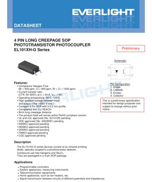
5.1 Pin Configuration
The 4-pin SOP package has the following pin arrangement:
- Input infrared LEDAnode
- 。Input infrared LED
- Cathode。
- Output phototransistorEmitter
Output phototransistor
Collector
。
This is the standard configuration for a phototransistor optocoupler.5.2 Package Dimensions and Pad LayoutThe device is described as a "compact 4-pin SOP with a 2.2 mm height". The PDF includes a "Package Dimensions" drawing and a "Recommended Land Pattern for Surface Mount". The land pattern recommendation is for reference only, and the datasheet explicitly advises designers to modify the pad dimensions based on their specific PCB fabrication process and thermal requirements. Proper pad design is crucial for reliable soldering and mechanical strength.
6. Soldering and Assembly Guide
The key parameters provided are
Welding temperature260°C, for 10 seconds. This aligns with the typical lead-free reflow soldering profile (IPC/JEDEC J-STD-020). Designers and manufacturers must ensure their reflow oven profile does not exceed this temperature duration to prevent damage to the internal epoxy molding compound and wire bonds. Standard handling procedures for moisture-sensitive devices (MSL rating, not specified in the provided text but should be checked in the full datasheet) should be followed, including baking if the package is exposed to ambient humidity exceeding its rated level.
- 7. Packaging and Ordering Information7.1 Model Naming Rules
- XThe model number follows the format:
- HEL101X H(Y)- VG
- EL101: Basic model.
- V: CTR rating (0, 1, 7, 8, 9).
- G: Indicates high-temperature operating capability.
: Tape and reel packaging option. Can be TA, TB, or none (indicating tube packaging).
: Optional suffix, indicating VDE safety certification.
- : Indicates halogen-free structure.Example: EL1018H-VG is a halogen-free version with CTR Grade 8 and VDE certification.
- 7.2 Packaging SpecificationThe device is available in two main package forms:
Tube
: 100 pieces per tube. Options include standard version or version with VDE certification.Tape and reel packaging
- EL: 3000 per reel. Two feed direction options (TA and TB) are provided. The datasheet includes detailed reel dimensions (Ao, Bo, Po, P, etc.) for automated placement machine programming.
- 7.3 Device IdentificationThe SOP package top is marked with the code:
- HEL 101X H Y WW V
- YManufacturer Code.
- WW101X
- VDevice Number (X indicates CTR Grade).
High temperature operation marking.
1-digit year code.
2-digit week code.
- Optional marking for VDE certified version.8. Application RecommendationsCC8.1 Typical Application Circuit
- Photocouplers can be used in two main modes:Digital switching/isolation
: The input LED is driven by a digital signal (e.g., from a microcontroller GPIO). The phototransistor output acts as a switch, pulling the line to ground or V through a pull-up resistor.
- . Switching time specifications determine the maximum data rate.Linear Signal Isolation: By operating the phototransistor in the amplification region (non-saturation region), it can be used to transmit analog signals. However, the nonlinearity of CTR and its variation with temperature make it challenging without additional compensation circuitry. For such tasks, dedicated linear optocouplers are more commonly used.8.2 Design ConsiderationsFInput Current Limitation:AlwaysAn external resistor is required in series with the input LED to set the forward current (I). Calculate RFlimitF= (VFdrive
- - V) / I
- . Ensure IL)does not exceed 50 mA DC.LCTR derating with temperatureL: Consider the decrease in CTR at high temperatures. Design the circuit so that it still operates correctly at the maximum operating temperature when using the minimum CTR of the selected grade.
- Output load resistor (R): The value of the collector pull-up resistor affects switching speed, power consumption, and noise immunity. A smaller R
provides faster switching speed but higher current consumption. R
= 100Ω test condition is used for characterization; actual values typically range between 1kΩ and 10kΩ.
- Noise Immunity:低耦合电容(<1pF)提供了良好的共模抑制。对于非常嘈杂的环境,确保布局干净,接地良好,并考虑在输出侧电源轨之间添加一个小旁路电容(例如0.1µF)。
- 9. Technical Comparison and AdvantagesThe EL101XH-G series stands out in the market through several key features:)Long creepage distance (8mm)
- Compared to standard SOP optocouplers, this extended creepage distance offers a significant advantage for applications requiring reinforced insulation or operation in polluted environments, as it reduces the risk of surface tracking.High isolation voltage (5000V
- RMS): This is a robust isolation rating suitable for industrial mains-connected equipment (e.g., 240V/480V systems).
- Compliant with halogen-free standards.: Meets environmental and regulatory requirements for reduced halogen content, which is increasingly important in green electronics.
Wide operating temperature range (-55°C to +125°C).
Exceeds the typical commercial range (0°C to 70°C), making it suitable for industrial, automotive, and military-grade applications.
Pending safety certifications
The datasheet lists certifications from UL, cUL, VDE, SEMKO, NEMKO, DEMKO, FIMKO, and CQC as "pending." This indicates the device is designed to meet these stringent international safety standards.
10. Frequently Asked Questions (Based on Technical Parameters)
Q1: What is the purpose of the long creepage distance?
A1: Creepage distance is the shortest path along the surface of the insulating package between two conductive parts (input and output pins). The 8mm distance increases protection against high-voltage arcing or tracking along the package surface, especially in humid or contaminated environments, thereby enhancing long-term reliability and safety.
Q2: Yaya za a zaɓi CTR darajar da ta dace?
A2: Zaɓi bisa ga ƙarfin kwararar da kuke da ita da kuma ƙarfin fitarwa da kuke buƙata. Idan microcontroller ɗinku zai iya ba da 5mA kawai, zaɓi babban matakin CTR (misali EL1019H) don samun isasshen ƙarfin fitarwa. Idan kuna da isasshen ƙarfin kwarara, ƙananan matakan na iya zama mafi arha. Koyaushe ƙirƙira bisa ga yanayin mafi munin (CTR mafi ƙanƙanta a zafin jiki mafi girma).Q3: Shin ana iya amfani da wannan don keɓe siginar AC?Q4: What is the difference between isolation voltage and collector-emitter voltage rating?A4: Isolation voltage (5000VRMS) is the packageBetween the input and output sides.
The dielectric withstand voltage. Collector-emitter voltage (80V) is during normal operation.
Can be applied across the output transistor itself.The maximum voltage. They are completely different parameters.
11. Practical Design Case Studies
- Scenario:In an industrial PLC module, isolate a 3.3V microcontroller GPIO signal to control a 24V relay coil on an independent power domain.FDesign Steps:FInput Side:MCU GPIO is 3.3V. Assuming the desired Iis 5mA, the typical V
- is 1.2V, calculate RlimitF= (3.3V - 1.2V) / 0.005A = 420Ω. Use a standard 430Ω resistor.
- CTR Selection:The base of the transistor driving the relay coil requires approximately 5mA. At IL=5mA, the required minimum CTR = (5mA / 5mA)*100% = 100%. To ensure operation at 125°C (where CTR is lower), select a grade with sufficient margin. EL1018H (minimum CTR 130%) is a good choice.
- Output Side:Connect the phototransistor collector to the 24V power supply via a pull-up resistor (R
Layout:
Keep input and output traces physically separated on the PCB. Place bypass capacitors close to the device pins. Follow the recommended pad layout for reliable soldering.
- This design provides robust isolation, protecting the sensitive microcontroller from transients generated by inductive relay coils.12. Working PrincipleAn optocoupler (or opto-isolator) is a device that uses light to transmit electrical signals between two isolated circuits. In the EL101XH-G series:Applied toInput pins (anode and cathode)
- The current causes the integrated
- Infrared light-emitting diode (LED)Emit photons.These photons propagate through the transparent insulating material within the package, typically molded epoxy.Photons strike.
- Output side的 pins.
- Silicon phototransistorCbase region.FLight energy generates electron-hole pairs in the base region, effectively acting as base current, causing the transistor to operate in its
Conducts between.
Output collector current (I
- ) is proportional to the input LED current (I), with the constant of proportionality being the Current Transfer Ratio (CTR).
- The key point is that the only connection between input and output is a beam of light, providing excellent electrical isolation determined by the properties of the insulating barrier and the internal distance between the LED and phototransistor chips.13. Industry Trends
- The market for isolation components such as optocouplers is evolving, driven by several key trends:Higher Speeds and Bandwidth:
- The growing demand for digital isolators and high-speed optocouplers capable of supporting communication protocols like USB, CAN FD, and Ethernet in isolated networks is pushing data rates into the tens and hundreds of Mbps.Integration:
- The trend is to integrate multiple isolated channels into a single package, or to combine isolation with other functions such as gate drivers for power MOSFETs/IGBTs.Enhanced Safety and Reliability Standards:
Detailed Explanation of LED Specification Terminology
Complete Interpretation of LED Technical Terminology
I. Core Indicators of Photoelectric Performance
| Terminology | Unit/Representation | Popular Explanation | Why It Matters |
|---|---|---|---|
| Luminous Efficacy | lm/W (lumens per watt) | The luminous flux emitted per watt of electrical power; higher values indicate greater energy efficiency. | It directly determines the energy efficiency rating of the luminaire and the electricity cost. |
| Luminous Flux | lm (lumen) | The total amount of light emitted by a light source, commonly known as "brightness". | Determines whether the luminaire is bright enough. |
| Viewing Angle | ° (degree), e.g., 120° | The angle at which luminous intensity drops to half, determining the beam width. | Affects the range and uniformity of illumination. |
| Correlated Color Temperature (CCT) | K (Kelvin), such as 2700K/6500K | Launin haske mai dumi ko sanyi, ƙananan ƙima sun fi rawaya/dumi, manyan ƙima sun fi fari/sanyi. | Yana ƙayyade yanayin hasken wuta da yanayin da ya dace. |
| Color Rendering Index (CRI / Ra) | Unitless, 0–100 | The ability of a light source to reproduce the true colors of objects, with Ra≥80 being preferable. | Affects color fidelity, used in high-demand places such as shopping malls and art galleries. |
| Color tolerance (SDCM) | MacAdam ellipse step, such as "5-step" | A quantitative metric for color consistency; a smaller step number indicates better color consistency. | Ensure no color variation among luminaires from the same batch. |
| Dominant Wavelength | nm (nanometer), e.g., 620nm (red) | Wavelength values corresponding to the colors of colored LEDs. | Determines the hue of monochromatic LEDs such as red, yellow, and green. |
| Spectral Distribution | Wavelength vs. Intensity Curve | Shows the intensity distribution of light emitted by an LED at each wavelength. | Affects color rendering and color quality. |
II. Electrical Parameters
| Terminology | Symbols | Popular Explanation | Design Considerations |
|---|---|---|---|
| Forward Voltage (Forward Voltage) | Vf | The minimum voltage required to light up an LED, similar to a "starting threshold". | The driving power supply voltage must be ≥ Vf; the voltages add up when multiple LEDs are connected in series. |
| Forward Current | If | The current value that makes the LED emit light normally. | Constant current drive is often used, as the current determines brightness and lifespan. |
| Maximum Pulse Current | Ifp | The peak current that can be withstood for a short period of time, used for dimming or flashing. | Pulse width and duty cycle must be strictly controlled to prevent overheating damage. |
| Reverse Voltage | Vr | Maximum reverse voltage that an LED can withstand; exceeding it may cause breakdown. | Reverse connection or voltage surges must be prevented in the circuit. |
| Thermal Resistance (Thermal Resistance) | Rth (°C/W) | The resistance to heat flow from the chip to the solder joint. A lower value indicates better heat dissipation. | High thermal resistance requires stronger heat dissipation design, otherwise junction temperature rises. |
| Electrostatic Discharge Immunity (ESD Immunity) | V (HBM), e.g., 1000V | Electrostatic discharge immunity; a higher value indicates greater resistance to electrostatic damage. | Anti-static measures must be implemented during production, especially for high-sensitivity LEDs. |
III. Thermal Management and Reliability
| Terminology | Key Indicators | Popular Explanation | Impact |
|---|---|---|---|
| Junction Temperature | Tj (°C) | The actual operating temperature inside the LED chip. | For every 10°C reduction, the lifespan may double; excessively high temperatures cause lumen depreciation and color shift. |
| Lumen Depreciation | L70 / L80 (hours) | The time required for the brightness to drop to 70% or 80% of its initial value. | Directly defining the "useful life" of an LED. |
| Lumen Maintenance | % (e.g., 70%) | The percentage of remaining brightness after a period of use. | Characterizes the ability to maintain brightness after long-term use. |
| Color Shift | Δu′v′ or MacAdam ellipse | The degree of color change during use. | Affects the color consistency of the lighting scene. |
| Thermal Aging | Material performance degradation | Degradation of packaging materials due to long-term high temperature. | Zai iya haifar da raguwar haske, canjin launi ko gazawar bude hanya. |
IV. Kullewa da Kayan aiki
| Terminology | Nau'o'in gama gari | Popular Explanation | Characteristics and Applications |
|---|---|---|---|
| Package Types | EMC, PPA, Ceramic | The housing material that protects the chip and provides optical and thermal interfaces. | EMC offers good heat resistance and low cost; ceramic provides superior heat dissipation and long lifespan. |
| Chip Structure | Front-side, Flip Chip | Chip electrode arrangement method. | Flip-chip offers better heat dissipation and higher luminous efficacy, suitable for high-power applications. |
| Phosphor coating. | YAG, silicate, nitride | Coated on the blue LED chip, partially converted to yellow/red light, mixed to form white light. | Different phosphors affect luminous efficacy, color temperature, and color rendering. |
| Lens/Optical Design | Flat, microlens, total internal reflection | The optical structure on the encapsulation surface controls the light distribution. | Determines the emission angle and the light distribution curve. |
V. Quality Control and Grading
| Terminology | Grading Content | Popular Explanation | Purpose |
|---|---|---|---|
| Luminous Flux Binning | Codes such as 2G, 2H | Group by brightness level, each group has a minimum/maximum lumen value. | Ensure consistent brightness for products in the same batch. |
| Voltage binning | Codes such as 6W, 6X | Grouped by forward voltage range. | Ease of matching drive power supply, improving system efficiency. |
| Color binning | 5-step MacAdam ellipse | Group by color coordinates to ensure colors fall within an extremely small range. | Ensure color consistency to avoid color unevenness within the same luminaire. |
| Color temperature grading | 2700K, 3000K, etc. | Group by color temperature, each group has a corresponding coordinate range. | Meet the color temperature requirements of different scenarios. |
VI. Testing and Certification
| Terminology | Standard/Test | Popular Explanation | Meaning |
|---|---|---|---|
| LM-80 | Lumen Maintenance Test | Long-term operation under constant temperature conditions, recording luminance attenuation data. | For estimating LED lifetime (in conjunction with TM-21). |
| TM-21 | Lifetime projection standard | Estimating lifespan under actual usage conditions based on LM-80 data. | Providing scientific life prediction. |
| IESNA Standard | Illuminating Engineering Society Standard | Covers optical, electrical, and thermal testing methods. | Industry-recognized testing basis. |
| RoHS / REACH | Environmental Certification | Ensure the product does not contain harmful substances (such as lead, mercury). | Entry requirements for the international market. |
| ENERGY STAR / DLC | Energy efficiency certification | Energy efficiency and performance certification for lighting products. | Commonly used in government procurement and subsidy programs to enhance market competitiveness. |