Table of Contents
- 1. Product Overview
- 2. Technical Specifications Deep Dive
- 2.1 Absolute Maximum Ratings
- 2.2 Electro-Optical Characteristics
- 2.2.1 Input Characteristics (Infrared LED)
- 2.2.2 Output Characteristics (Phototransistor)
- 2.2.3 Transfer Characteristics
- 3. Grading System Explanation
- 4. Performance Curve Analysis
- 5. Mechanical and Package Information
- 6. Soldering and Assembly Guidelines
- 7. Packaging and Ordering Information
- 8. Application Recommendations
- 8.1 Typical Application Scenarios
- 8.2 Design Considerations
- 9. Kwatancen Fasaha da Fa'idodi
- 10. Tambayoyin da ake yawan yi (Dangane da Ma'auni na Fasaha)
- 11. Practical Design Example
- 12. Operating Principle
- 13. Technology Trends
1. Product Overview
The EL111X-G series represents a family of phototransistor-based photocouplers (optocouplers) designed for applications requiring robust electrical isolation and signal transmission between circuits of different potentials. The core function of this device is to transfer an electrical signal using light, providing galvanic isolation between the input (infrared emitting diode) and output (phototransistor detector) sides. This isolation is critical for protecting sensitive circuitry from high voltages, noise, and ground loops.
The series is characterized by its compact 5-pin Small Outline Package (SOP) with a low profile of 2.0 mm, making it suitable for space-constrained PCB designs. A key distinguishing feature is its 8mm long creepage distance, which enhances reliability and safety in high-voltage environments by increasing the surface distance between conductive parts along the package body. The devices are constructed using compound materials free from halogens (Bromine <900 ppm, Chlorine <900 ppm, Br+Cl <1500 ppm) and antimony trioxide (Sb2O3), aligning with environmental and safety regulations.
2. Technical Specifications Deep Dive
2.1 Absolute Maximum Ratings
These ratings define the limits beyond which permanent damage to the device may occur. Operation under these conditions is not guaranteed.
- Input Forward Current (IF): 60 mA (Continuous). The peak forward current for a 1µs pulse is significantly higher at 1.5 A, allowing for brief overcurrent conditions during switching.
- Input Reverse Voltage (VR): 6 V. Exceeding this voltage in reverse bias can damage the input LED.
- Output Collector-Emitter Voltage (VCEO): 80 V. This is the maximum voltage that can be applied across the output transistor when the base is open.
- Output Collector Current (IC): 50 mA.
- Total Power Dissipation (PTOT): 250 mW. This is the combined maximum power dissipation for both input and output sides.
- Isolation Voltage (VISO): 5000 Vrms for 1 minute at 40-60% relative humidity. This is a critical safety parameter, tested with input pins (1,2) shorted together and output pins (3,4,5) shorted together.
- Operating Temperature (TOPR): -55°C to +110°C.
- Soldering Temperature (TSOL): 260°C for 10 seconds, compliant with typical reflow soldering profiles.
2.2 Electro-Optical Characteristics
These parameters define the device's performance under normal operating conditions (Ta=25°C unless noted).
2.2.1 Input Characteristics (Infrared LED)
- Forward Voltage (VF): Maximum 1.5 V at IF = 50 mA. A typical value would be lower, around 1.1-1.3V.
- Reverse Current (IR): Maximum 10 µA at VR = 6 V.
- Input Capacitance (Cin): Typical 50 pF at 1 kHz. This affects high-frequency switching performance.
2.2.2 Output Characteristics (Phototransistor)
- Collector-Emitter Dark Current (ICEO): Maximum 100 nA at VCE = 20V, IF = 0mA. This is the leakage current when the LED is off.
- Collector-Emitter Breakdown Voltage (BVCEO): Minimum 80 V at IC = 0.1mA.
- Collector-Emitter Saturation Voltage (VCE(sat)): Maximum 0.4 V at IF = 10mA, IC = 1mA. A low saturation voltage is desirable for output stages driving logic-level inputs.
2.2.3 Transfer Characteristics
These parameters describe the coupling efficiency and speed between input and output.
- Current Transfer Ratio (CTR): This is the ratio of output collector current (IC) to input forward current (IF), expressed as a percentage. The EL111X-G series is offered in multiple CTR grades (ranks), each with a specified min/max range at defined test conditions. This allows designers to select a device with consistent gain for their application.
- EL1110, EL1116, EL1117, EL1118, EL1119: Tested at IF = 5mA, VCE = 5V. Ranges vary from 50-600% (EL1110) to 200-400% (EL1119).
- EL1112, EL1113, EL1114: Tested at IF = 10mA, VCE = 5V. Ranges are 63-125%, 100-200%, and 160-320% respectively. These parts also have specified minimum CTR values at IF = 1mA.
- Isolation Resistance (RIO): Minimum 5 x 10¹⁰ Ω i 500V DC. Wannan yana nuna babban juriyar DC tsakanin gefuna masu keɓewa.
- Ƙarfin Ƙarfin Ruwa (CIO): Matsakaicin 1.0 pF a 1 MHz. Wannan ƙaramin ƙarfin yana taimakawa wajen kiyaye babban juriya na wucin gadi na gama-gari (CMTI) ta hanyar rage haɗin ƙarfin ƙarfin amo.
- Lokutan Sauya: Measured with VCE = 5V, IC = 5mA, RL = 100Ω.
- Turn-on Time (ton): Typical 4 µs.
- Turn-off Time (toff): Typical 3 µs.
- Rise Time (tr): Typical 2 µs, Maximum 18 µs.
- Fall Time (tf): Typical 3 µs, Maximum 18 µs.
3. Grading System Explanation
The primary grading system for the EL111X-G series is based on the Current Transfer Ratio (CTR). Different part numbers (denoted by the 'X' in EL111X) correspond to specific, guaranteed ranges of CTR measured under standard conditions (IF=5mA or 10mA, VCE=5V). This allows designers to:
- Ensure Circuit Stability: Selecting a tighter CTR range (e.g., EL1117: 80-160%) provides more predictable output current for a given input current, reducing the need for wide-tolerance biasing circuits.
- Optimize Power Consumption: For a required output current, a higher CTR device (e.g., EL1119) can be driven with a lower input LED current, saving power on the primary side.
- Match Design Requirements: Different applications may require different gain. Logic interface circuits might use a standard CTR device, while analog signal transmission might benefit from a higher, more linear CTR part.
The ordering information clearly defines this grading with the 'X' character (0, 2, 3, 4, 6, 7, 8, 9).
4. Performance Curve Analysis
While specific graphical curves are referenced in the datasheet ("Typical Electro-Optical Characteristics Curves"), their typical behavior can be described based on phototransistor photocoupler principles:
- CTR vs. Forward Current (IF): CTR is not constant. It typically peaks at a moderate forward current (often around 5-10mA for these devices) and may decrease at very low or very high currents due to LED efficiency and transistor saturation effects.
- CTR vs. Temperature: CTR yawanci yana da ingantaccen zafin jiki coefficient; yana raguwa yayin da haɗin haɗin zafi ya karu. Masu zane dole ne su yi la'akari da wannan ragewa a kan kewayon zafin aiki.
- Fitarwar Halin yanzu (IC) da Collector-Emitter Voltage (VCE): Phototransistor yana kama da tushen halin yanzu don ƙayyadadden halin yanzu na LED har sai ya shiga cikakken yanayi. Yankin cikakken yanayi yana da siffa ta ƙaramin VCE(sat) as specified.
- Switching Time vs. Load Resistance (RL): Switching times (tr, tf) are highly dependent on the load resistor and any parasitic capacitance. A smaller RL generally provides faster fall times but reduces output swing and increases power dissipation.
5. Mechanical and Package Information
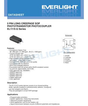
The device uses a 5-pin SOP (Small Outline Package) with a height of 2.0 mm. The pin configuration is standardized:
- Anode (Input LED+)
- Cathode (Input LED-)
- Emitter (Phototransistor)
- Collector (Phototransistor)
- Base (Phototransistor, typically left open or connected for speed-up techniques)
The package includes a recommended pad layout for surface mount assembly, which is crucial for achieving reliable solder joints and proper mechanical stability during reflow. The 8mm long creepage distance is a physical design feature of the package mold that increases the surface distance between the input and output pins, directly contributing to the high 5000Vrms isolation rating and compliance with safety standards.
6. Soldering and Assembly Guidelines
The device is rated for a maximum soldering temperature of 260°C for 10 seconds. This aligns with standard lead-free reflow soldering profiles (IPC/JEDEC J-STD-020). Key considerations include:
- Use the recommended PCB land pattern to prevent tombstoning or misalignment.
- Avoid excessive solder paste which could cause bridging between the closely spaced pins or short the creepage gap.
- Follow standard moisture sensitivity level (MSL) handling procedures for plastic packages, typically involving baking if the device has been exposed to ambient humidity beyond its rated floor life.
- Storage temperature range is -55°C to +125°C.
7. Packaging and Ordering Information
The product is available in multiple packaging options to suit different production scales:
- Tube: 100 units per tube (Standard or with VDE option).
- Tape and Reel: 3000 units per reel. Two reel options (TA, TB) are available, likely differing in tape width or component orientation. Both can be combined with the VDE safety approval option.
The part number structure is: EL111X(Y)-VG
- EL111: Base part number.
- X: CTR Rank (0,2,3,4,6,7,8,9).
- Y: Tape & Reel option (TA, TB, or blank for tube).
- V: Optional VDE safety approval marking.
- G: Denotes Halogen-free construction.
Device marking on the package includes a code for year and week of manufacture, along with the device number and optional VDE indicator.
8. Application Recommendations
8.1 Typical Application Scenarios
- Programmable Logic Controller (PLC) I/O Modules: Isolating digital signals from field sensors/actuators from the central processing unit.
- Switching Power Supplies: Providing feedback isolation in flyback or other isolated converter topologies.
- Industrial Communication Interfaces: Isolating RS-485, CAN, or other serial bus lines to prevent ground loops and enhance noise immunity.
- Medical Equipment: Isolating patient-connected circuits from mains-powered sections, where safety isolation is paramount.
- Home Appliance Control: Isolating low-voltage microcontroller signals from triac-driven AC motor or heater circuits in appliances like fan heaters.
- Measurement Instruments: Isolating analog signal conditioning stages from data acquisition systems.
8.2 Design Considerations
- Input Current Limiting: Always use a series resistor to limit the LED forward current (IF) to the desired value, calculated as (Supply Voltage - VF) / IF. Do not exceed the absolute maximum ratings.
- CTR Degradation: Be aware that CTR can degrade over the lifetime of the device, especially if operated at high temperatures or high LED currents. Derate the initial CTR value in critical designs.
- Speed vs. Current Trade-off: Higher IF generally improves switching speed but increases power dissipation and may accelerate CTR degradation. The load resistor RL also critically affects switching speed and output voltage swing.
- Noise Immunity: The high isolation resistance and low coupling capacitance provide good common-mode rejection. For very noisy environments, ensure a clean layout with proper grounding and consider adding bypass capacitors near the device pins.
- Using the Base Pin (Pin 5): Leaving the base open is standard. Connecting a resistor between base and emitter can reduce the phototransistor's gain but significantly improve its switching speed (especially turn-off time) by providing a path to remove stored charge.
9. Kwatancen Fasaha da Fa'idodi
The EL111X-G series differentiates itself in the photocoupler market through several key features:
- Long Creepage SOP Package: The 8mm creepage in a standard SOP footprint offers a superior isolation rating (5000Vrms) compared to many standard SOP photocouplers, often rated for 2500Vrms or 3750Vrms. This provides a safety margin and meets stricter isolation requirements without moving to larger packages.
- Comprehensive Safety Approvals: The series carries approvals from major international safety agencies (UL, cUL, VDE, SEMKO, NEMKO, DEMKO, FIMKO, CQC), simplifying compliance for global products.
- Environmental Compliance: Halogen-free and RoHS-compliant construction addresses environmental regulations and supply chain requirements.
- Wide CTR Selection: The multiple, clearly defined CTR grades offer designers flexibility to optimize for gain, power, or cost.
10. Tambayoyin da ake yawan yi (Dangane da Ma'auni na Fasaha)
- Q: What is the purpose of the long creepage distance?
A: Creepage is the shortest distance between two conductive parts along the surface of the insulating package. An 8mm creepage distance significantly increases the breakdown path for surface contamination (dust, moisture), which is essential for achieving and maintaining the high 5000Vrms isolation voltage rating, especially in humid or polluted environments. - Q: How do I choose the right CTR grade?
A: Zaɓi bisa ga ƙarfin fitarwa da ake buƙata a cikin da'irarka da ƙarfin turawa na shigarwa. Idan microcontroller GPIO pin ɗinka zai iya samar da 5mA kawai, zaɓi mafi girman CTR grade (misali EL1119) don samun isasshen ƙarfin fitarwa. Idan kana buƙatar ci gaba mai daidaito, mai iya hasashe don analog sensing, zaɓi grade mai ƙaramin kewayon (misali EL1117). Koyaushe ka tuntubi ƙananan/mafi girman ƙimomi a takamaiman wurin aiki. - Q: Zan iya amfani da wannan don watsa siginar analog?
A: I, amma tare da sharuɗɗa. Amsar phototransistor ba ta da cikakkiyar layi, kuma CTR ya bambanta da zafin jiki da ƙarfin halin yanzu. Ya fi dacewa ga ƙananan mitoci ko siginoyin analog da aka wakilta ta hanyar dijital (kamar PWM). Don keɓancewar analog mai daidaito, keɓantaccen optocouplers na layi ko masu ƙara keɓewa sun fi dacewa. - Q: What is the difference between the TA and TB tape & reel options?
A: Takardar bayanai tana nuna zane-zane guda biyu daban-daban na girman tef. Babban bambanci yana yiwuwa shine yanayin kayan aiki a cikin aljihun tef ("Hanyar ciyarwa daga reel") da yuwuwar faɗin tef. Zaɓin TB yana da girman Ko na 2.25mm. Tuntubi masana'anta ko cikakkun ƙayyadaddun tef don dacewar injin ɗauka da sanyawa. - Q: Ta yaya zafin jiki ke shafar aiki?
A: Temperature primarily affects CTR (decreases with increasing temperature) and the forward voltage VF of the input LED (also decreases). Switching speeds may also vary. Designs intended for the full -55°C to +110°C range must account for these variations, especially the CTR derating.
11. Practical Design Example
Scenario: Isolating a 3.3V microcontroller GPIO signal to control a 12V relay on the isolated side. The relay coil requires 30mA to activate.
Design Steps:
- Choose CTR Grade: Da ake bukata IC shine 30mA. Microcontroller na iya samar da ~10mA. Ana buƙatar CTR = (30mA / 10mA) * 100% = 300%. A IF=10mA, EL1114 yana da kewayon CTR na 160-320%. Muna zaɓar EL1114, tare da sanin cewa a mafi ƙarancin CTR (160%), IC zai zama 16mA, wanda ƙila bai isa ba. Muna iya buƙatar tuƙi LED da ƙarfi ko zaɓi wani daraja/na'ura daban.
- Recalculate with EL1119: EL1119 is rated at IF=5mA. CTR range is 200-400%. If we drive it at IF=7.5mA (within rating), using the typical CTR, we can expect IC around 22.5-30mA. This is borderline. A better solution is to use a transistor on the output to drive the relay, using the photocoupler only as a logic-level isolator.
- Input Resistor Calculation (using EL1114 at IF=10mA): Assume VF ~ 1.2V. Microcontroller voltage is 3.3V. Rlimit = (3.3V - 1.2V) / 0.01A = 210 Ω. Use a standard 200 Ω resistor.
- Output Side: Connect the phototransistor collector to the 12V supply via the relay coil. The emitter connects to ground. Place a flyback diode inversely across the relay coil. The phototransistor will saturate when on, with VCE(sat) < 0.4V, applying nearly the full 12V across the relay.
- Speed Consideration: The relay is slow, so the photocoupler's ~4µs turn-on time is irrelevant. No base resistor is needed for speed-up.
12. Operating Principle
A photocoupler, or optocoupler, is a device that transfers electrical signals between two isolated circuits using light. In the EL111X-G series:
- An electrical current is applied to the input pins (1-Anode, 2-Cathode), forward-biasing the internal infrared light-emitting diode (IRED).
- The IRED emits infrared light proportional to the forward current.
- This light travels across a transparent insulating gap (typically a molded plastic) and strikes the base region of a silicon phototransistor on the output side.
- The incident light generates electron-hole pairs in the base, effectively acting as a base current. This causes the phototransistor to conduct between its collector (pin 4) and emitter (pin 3).
- The resulting output collector current (IC) is approximately proportional to the input LED current (IF), with the proportionality constant being the Current Transfer Ratio (CTR).
- The key is that the only connection between input and output is the light beam; there is no electrical conductive path. This provides the galvanic isolation, blocking high voltages, ground potential differences, and noise.
13. Technology Trends
Photocoupler technology continues to evolve alongside system demands:
- Higher Speed: Demand for faster digital isolation in motor drives, communications, and ADCs drives development of photocouplers with faster switching times (nanosecond range) and higher common-mode transient immunity (CMTI).
- Integration: There is a trend towards integrating additional functionality, such as gate drivers for IGBTs/MOSFETs, error amplifiers for power supplies, or even digital isolators with multiple channels in one package.
- Improved Reliability and Lifetime: Focus on materials and design to reduce long-term CTR degradation, especially for high-temperature automotive and industrial applications.
- Miniaturization: While maintaining or improving isolation ratings, packages continue to shrink (e.g., ultra-miniature SOP, wafer-level packaging) to save board space.
- Teknolojioj Alternativaj: Fotokupliloj frontas konkurencon de aliaj izolaj teknologioj kiel kapacitivaj izoliloj (uzantaj SiO2 barilojn) kaj magnetaj (transformil-bazitaj) izoliloj, kiuj povas oferi pli altan rapidon, pli malaltan povumon kaj pli bonan integriĝon. Tamen, fotokupliloj restas ĉefaj en multaj aplikoj pro ilia simpleco, alta tensiokapablo, bone komprenata fidindeco kaj kostefikeco por normrapidaj postuloj.
La serio EL111X-G, kun ĝia fokuso sur alta izola tensio en kompakta, media-konforma pakaĵo, traktas la konstatan bezonon pri fidinda, sekurec-aprobita signalizolo en vasta gamo de industriaj kaj konsumantaj aplikoj.
LED Specification Terminology
Complete explanation of LED technical terms
Photoelectric Performance
| Term | Unit/Representation | Simple Explanation | Why Important |
|---|---|---|---|
| Luminous Efficacy | lm/W (lumens per watt) | Haske a kowane watt na wutar lantarki, mafi girma yana nufin mafi ingancin makamashi. | Kai tsaye yana ƙayyade matakin ingancin makamashi da farashin wutar lantarki. |
| Luminous Flux | lm (lumens) | Total light emitted by source, commonly called "brightness". | Determines if the light is bright enough. |
| Viewing Angle | ° (degrees), e.g., 120° | Angle where light intensity drops to half, determines beam width. | Affects illumination range and uniformity. |
| CCT (Color Temperature) | K (Kelvin), e.g., 2700K/6500K | Mwangaza wa joto/baridi, thamani za chini ni manjano/joto, za juu ni nyeupe/baridi. | Huamua mazingira ya taa na matukio yanayofaa. |
| CRI / Ra | Unitless, 0–100 | Ability to render object colors accurately, Ra≥80 is good. | Affects color authenticity, used in high-demand places like malls, museums. |
| SDCM | MacAdam ellipse steps, e.g., "5-step" | Color consistency metric, smaller steps mean more consistent color. | Ensures uniform color across same batch of LEDs. |
| Dominant Wavelength | nm (nanometers), e.g., 620nm (red) | Wavelength corresponding to color of colored LEDs. | Determines hue of red, yellow, green monochrome LEDs. |
| Spectral Distribution | Wavelength vs intensity curve | Shows intensity distribution across wavelengths. | Affects color rendering and quality. |
Electrical Parameters
| Term | Symbol | Simple Explanation | Design Considerations |
|---|---|---|---|
| Forward Voltage | Vf | Minimum voltage to turn on LED, like "starting threshold". | Driver voltage must be ≥Vf, voltages add up for series LEDs. |
| Forward Current | If | Current value for normal LED operation. | Usually constant current drive, current determines brightness & lifespan. |
| Max Pulse Current | Ifp | Peak current tolerable for short periods, used for dimming or flashing. | Pulse width & duty cycle must be strictly controlled to avoid damage. |
| Reverse Voltage | Vr | Max reverse voltage LED can withstand, beyond may cause breakdown. | Circuit must prevent reverse connection or voltage spikes. |
| Thermal Resistance | Rth (°C/W) | Resistance to heat transfer from chip to solder, lower is better. | High thermal resistance requires stronger heat dissipation. |
| ESD Immunity | V (HBM), e.g., 1000V | Ability to withstand electrostatic discharge, higher means less vulnerable. | Anti-static measures needed in production, especially for sensitive LEDs. |
Thermal Management & Reliability
| Term | Key Metric | Simple Explanation | Impact |
|---|---|---|---|
| Junction Temperature | Tj (°C) | Yanzu aiki zazzabi a cikin LED chip. | Kowane raguwar 10°C na iya ninka tsawon rayuwa; yana da yawa yana haifar da lalacewar haske, canjin launi. |
| Lumen Depreciation | L70 / L80 (hours) | Time for brightness to drop to 70% or 80% of initial. | Directly defines LED "service life". |
| Lumen Maintenance | % (e.g., 70%) | Percentage of brightness retained after time. | Indicates brightness retention over long-term use. |
| Color Shift | Δu′v′ or MacAdam ellipse | Iyipada awọ nigba lilo. | O nife si iṣeṣi awọ ninu awọn iboju itansẹ. |
| Thermal Aging | Material degradation | Deterioration due to long-term high temperature. | May cause brightness drop, color change, or open-circuit failure. |
Packaging & Materials
| Term | Common Types | Simple Explanation | Features & Applications |
|---|---|---|---|
| Package Type | EMC, PPA, Ceramic | Housing material protecting chip, providing optical/thermal interface. | EMC: good heat resistance, low cost; Ceramic: better heat dissipation, longer life. |
| Usoro Chip | Ihu, Flip Chip | Chip electrode arrangement. | Flip chip: better heat dissipation, higher efficacy, for high-power. |
| Phosphor Coating | YAG, Silicate, Nitride | Covers blue chip, converts some to yellow/red, mixes to white. | Phosphors ya daban-daban suna tasiri aikin, CCT, da CRI. |
| Lens/Optics | Flat, Microlens, TIR | Optical structure on surface controlling light distribution. | Determines viewing angle and light distribution curve. |
Quality Control & Binning
| Term | Binning Content | Simple Explanation | Purpose |
|---|---|---|---|
| Luminous Flux Bin | Code e.g., 2G, 2H | Grouped by brightness, each group has min/max lumen values. | Ensures uniform brightness in same batch. |
| Voltage Bin | Code e.g., 6W, 6X | Grouped by forward voltage range. | Yana taimaka da daidaita direbobi, yana inganta ingancin tsarin. |
| Kwandon Launi | 5-step MacAdam ellipse | Grouped by color coordinates, ensuring tight range. | Guarantees color consistency, avoids uneven color within fixture. |
| CCT Bin | 2700K, 3000K etc. | Grouped by CCT, each has corresponding coordinate range. | Meets different scene CCT requirements. |
Testing & Certification
| Term | Standard/Test | Simple Explanation | Significance |
|---|---|---|---|
| LM-80 | Lumen maintenance test | Long-term lighting at constant temperature, recording brightness decay. | Used to estimate LED life (with TM-21). |
| TM-21 | Life estimation standard | Inakadiria maisha chini ya hali halisi kulingana na data ya LM-80. | Inatoa utabiri wa kisayansi wa maisha. |
| IESNA | Illuminating Engineering Society | Covers optical, electrical, thermal test methods. | Industry-recognized test basis. |
| RoHS / REACH | Environmental certification | Ensures no harmful substances (lead, mercury). | Market access requirement internationally. |
| ENERGY STAR / DLC | Energy efficiency certification | Energy efficiency and performance certification for lighting. | Used in government procurement, subsidy programs, enhances competitiveness. |