Tari
- 1. Product Overview
- 1.1 Core Features and Advantages
- 1.2 Target Market and Applications
- 2. In-depth Technical Parameter Analysis
- 2.1 Absolute Maximum Ratings
- 2.2 Photoelectric Characteristics (Ta=25°C)
- 2.3 Collector Current Grading Range
- 3. Performance Curve Analysis
- 3.1 Electrical Characteristics
- 3.2 Temperature Characteristics
- 3.3 Optical and Spatial Characteristics
- 4. Mechanical and Packaging Information
- 4.1 Package Dimensions
- 4.2 Recommended PCB Land Pattern
- 4.3 Polarity and Orientation
- 5. Guidelines for Welding, Assembly, and Storage
- 5.1 Reflow Soldering Conditions
- 5.2 Moisture Sensitivity and Storage (MSL 3)
- 6. Packaging and Ordering Information
- 6.1 Tape and Reel Specifications
- 6.2 Packaging Program
- 7. Application Design Considerations
- 7.1 Typical Application Circuit
- 7.2 Design Factors for Reliable Sensing
- 8. Technical Comparison and Differentiation
- 9. Frequently Asked Questions (Based on Technical Specifications)
- 10. Working Principle
1. Product Overview
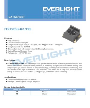
ITR1502SR40A/TR8 is a highly integrated, surface-mount reflective photointerrupter designed for non-contact sensing applications. It integrates an infrared emitter and a silicon phototransistor detector within a compact black transparent lens package. The device is designed for reliable object presence or motion detection, with a nominal optimal sensing distance of 4 mm. Its leadless package is specifically designed to be compatible with modern reflow soldering processes, making it suitable for high-volume automated assembly.
1.1 Core Features and Advantages
- High Sensitivity:Silicon phototransistors generate a strong electrical response to reflected infrared light, enabling reliable detection.
- Visible Light Cutoff:Black transparent lens material can effectively block ambient visible light, minimizing the possibility of false triggers caused by ambient light sources.
- Compact Form Factor:Dimensions of 4.0 mm x 3.0 mm x 2.0 mm, ideal for space-constrained PCB designs.
- Reflow solderable:Leadless (tape and reel) package supports standard SMT assembly and can withstand peak soldering temperatures up to 260°C for 5 seconds.
- Environmental compliance:该器件符合无卤标准(Br < 900ppm,Cl < 900ppm,Br+Cl < 1500ppm)、欧盟 REACH 法规,并且符合 RoHS 标准。
- Long Focal Length:Within its package family, it offers a relatively long optimal sensing distance of 4 mm.
1.2 Target Market and Applications
This component is designed for engineers in consumer electronics, office automation, and industrial control systems who require reliable, low-cost object sensing. Its primary function is to detect the presence, absence, or passage of an object without physical contact.
- Printers and Copiers:Detect paper jams, paper tray status, or media presence.
- Optical storage drive (e.g., CD/DVD):Sense the disc tray position or detect the presence of a disc.
- Projector and display:Monitor filter status, cover position, or other internal mechanisms.
- Vending machines and kiosks:Detection of product distribution or user interaction.
- Household appliances:Position sensing in smart locks, coffee machines, or other automated devices.
2. In-depth Technical Parameter Analysis
The performance of the ITR1502SR40A/TR8 is defined by a comprehensive set of electrical and optical parameters. Understanding these parameters is crucial for proper circuit design and reliable system operation.
2.1 Absolute Maximum Ratings
These ratings define the stress limits that may cause permanent damage to the device. Operation under these conditions is not guaranteed.
- Input power dissipation (Pd):75 mW at free-air temperature ≤25°C.
- Forward Current (IF):50 mA (continuous).
- Peak Forward Current (IFP):At a duty cycle of 1%, a pulse ≤100μs can reach 1 A.
- Reverse Voltage (VR):5 V.
- Collector Power Dissipation (PC):75 mW.
- Collector Current (IC):25 mA.
- Collector-emitter voltage (VCEO):30 V.
- Emitter-Collector Voltage (VECO):5 V.
- Operating Temperature (Topr):-25°C to +85°C.
- Storage temperature (Tstg):-40°C to +100°C.
- Pin soldering temperature:260°C for 5 seconds at 1/16 inch from the body.
2.2 Photoelectric Characteristics (Ta=25°C)
These are the guaranteed performance parameters under specified test conditions.
Input (Infrared Emitter - IR GaAs Chip):
- Forward Voltage (VF):Typical 1.2V, Maximum 1.4V at IF= 20 mA. This defines the voltage drop across the LED when driven.
- Reverse Current (IR):At VR= 6V, maximum 10 μA.
- Peak wavelength (λP):At IF= 10 mA, it is 940 nm (nominal). This belongs to the near-infrared spectrum and is invisible to the human eye.
Output (Phototransistor - Silicon Chip):
- Dark Current (ICEO):Typical 1 nA, at VCE= 20V maximum 100 nA. This is the leakage current when no light is incident on the detector.
- Transfer characteristics - Collector current (IC(ON)):Under test conditions: VCE=2V, IF=4mA, with a reflective target distance d=4mm, minimum 60 μA, typical value, maximum 450 μA. This is the key parameter indicating sensitivity.
- Transfer Characteristic - Off-state Current (IC(OFF)):Under the same test conditions but without a reflective (or absorptive) target, the maximum is 600 nA.
- Response time (tr, tf):Typical rise and fall times are both 20 μs, maximum 100 μs. Test conditions: VCE=2V, IC=100μA, RL=1kΩ, d=4mm. This defines the switching speed.
Note: Operating dark current may be affected by the surrounding environment (e.g., ambient infrared light sources).
2.3 Collector Current Grading Range
Devices are categorized based on their measured collector current (IC(ON)) are graded. This allows designers to select components with consistent sensitivity for their applications.
- Grade A:60 μA ≤ IC(ON)< 120 μA
- B grade:100 μA ≤ IC(ON)< 220 μA
- C grade:180 μA ≤ IC(ON)< 350 μA
- D grade:310 μA ≤ IC(ON)≤ 450 μA
3. Performance Curve Analysis
The provided characteristic curves offer valuable insights into the device's behavior under various conditions, which is crucial for robust system design.
3.1 Electrical Characteristics
Forward Current vs. Forward Voltage:This curve shows the typical IV characteristics of an infrared emitter LED. It is nonlinear, similar to a standard diode. At 20mA, the typical forward voltage is about 1.2V.
Forward Current vs. Collector Current:This is the transfer curve, showing the output current (IC) How to follow the input LED drive current (IF) increase. Within the operating region, the relationship is approximately linear, demonstrating the device's gain.
Collector current vs. Collector-emitter voltage:This set of curves shows at different ICAt various levels (e.g., 5mA, 10mA, 20mA, 50mA), IFvaries with VCE. It illustrates that the phototransistor acts as a current source; beyond a certain VCE(saturation voltage, typically low), ICIt is primarily determined by the incident light (and thus IF).
3.2 Temperature Characteristics
Forward Voltage vs. Ambient Temperature:The forward voltage of an LED has a negative temperature coefficient, decreasing slightly as temperature increases (from approximately 1.21V at -20°C to 1.16V at 80°C).
Relative Collector Current vs. Ambient Temperature:This is a key curve. The collector current (sensitivity) decreases significantly as temperature increases. At 80°C, the relative output is only about 80% of its value at 25°C. This must be considered in designs operating at high temperatures to ensure sufficient signal margin.
Collector Dark Current vs. Ambient Temperature:Dark current increases exponentially with temperature (from approximately 0.1nA at -40°C to nearly 1000nA at 100°C). In high-temperature applications, this increased leakage current can become a significant component of the signal, potentially degrading the signal-to-noise ratio.
Power Consumption vs. Ambient Temperature:This derating curve shows that when the ambient temperature exceeds 25°C, the maximum allowable power dissipation of the device decreases linearly, reaching 0 mW at 100°C.
3.3 Optical and Spatial Characteristics
Wavelength Spectrum:Relative radiation intensity curve shows the emitter's output center at 940 nm, with a typical spectral width. The black transparent lens effectively transmits this infrared light while blocking shorter visible wavelengths.
Relative collector current vs. Z-axis travel distance (mirror):This curve defines the sensing profile. The output current is highest when the reflective target is at the optimal distance (4mm). The signal attenuates as the target moves closer or farther away, defining the actual sensing window. The curve shape is roughly Gaussian.
Switching time vs. load resistance:Rise time (tr) and fall time (tf) both increase with the increase of load resistance (RL). To achieve the fastest switching speed, a lower RL, but this also leads to a reduction in the output voltage swing. Designers must strike a balance between speed and signal level.
4. Mechanical and Packaging Information
4.1 Package Dimensions
The device is housed in a compact leadless surface-mount package measuring 4.0 mm in length, 3.0 mm in width, and 2.0 mm in height. Key dimensional notes include:
- All dimensions are in millimeters.
- Unless otherwise specified, the tolerance is ±0.1mm.
- Pin pitch is measured at the point where the pins exit the package.
- The product weight is approximately 0.025 grams.
4.2 Recommended PCB Land Pattern
Recommended pad layout is provided to ensure reliable soldering and mechanical stability. A key design rule is emphasized: the amount of solder must be carefully controlled to prevent solder wicking or seepage into the gap between the PCB and the package body. Excessive solder in this area can create stress, impair functionality, or reduce long-term reliability. Pad design typically includes thermal connections and sufficient copper area for a strong bond.
4.3 Polarity and Orientation
The device has a marked orientation (usually a dot or notch on the top surface) indicating pin 1. The pin configuration for such devices is standard: the infrared emitter anode and cathode form one pair, and the phototransistor collector and emitter form another pair. The datasheet diagram must be consulted for the exact pin assignment. Incorrect orientation will prevent the device from functioning.
5. Guidelines for Welding, Assembly, and Storage
5.1 Reflow Soldering Conditions
ITR1502SR40A/TR8 is rated for lead-free reflow soldering processes. A recommended temperature profile is provided, which typically includes:
- Preheating/Ramp-up:Controlled heating to activate the flux.
- Soak Zone:Maintain at a temperature below the liquidus for a period to ensure uniform heating.
- Reflow Zone:Peak temperature should not exceed 260°C, and the time above 240°C should be limited (e.g., 30-60 seconds).
- Cooling:Controlled cooling period.
Important note:The same device should not undergo more than two reflow soldering cycles to avoid thermal stress damage to internal components and molding compound.
5.2 Moisture Sensitivity and Storage (MSL 3)
This package is moisture sensitive. The following procedures must be followed to prevent "popcorn" phenomenon (package cracking due to vapor pressure during reflow).
- Storage in unopened package:Store under conditions of ≤30°C and ≤90% RH. Use within one year from the date of shipment.
- After opening:Store under conditions of ≤30°C and ≤70% RH.
- Pot life:Devices must be soldered within 168 hours (7 days) after the moisture barrier bag is opened.
- Baking:If the floor life is exceeded or the humidity indicator card (desiccant) shows saturation, the devices should be baked at 60°C ±5°C for 24 hours to remove absorbed moisture before use.
6. Packaging and Ordering Information
6.1 Tape and Reel Specifications
This device is supplied in tape and reel packaging compliant with the EIA-481 standard, suitable for automated surface-mount assembly.
- Package Quantity:800 pieces per reel.
- Reels per box:38 rolls per outer carton.
- Outer carton dimensions:409 mm (A) x 245 mm (B) x 360 mm (C).
The reel has specific directional labels indicating the forward direction. Detailed reel dimensions (core diameter, reel width, etc.) are provided to ensure compatibility with mounting equipment.
6.2 Packaging Program
Reels are packaged in sealed aluminum foil moisture barrier bags. Each bag contains a desiccant pack and a humidity indicator card to monitor moisture levels. Multiple bags are then placed into a master shipping carton.
7. Application Design Considerations
7.1 Typical Application Circuit
Basic application circuit involves two main parts:
- Transmitter drive:A current-limiting resistor in series with the infrared LED. The resistor value is calculated as Rlimit= (VCC- VF) / IF. For example, using a 5V power supply, expecting IFto be 20mA: Rlimit= (5V - 1.2V) / 0.02A = 190Ω (use a standard 200Ω resistor). The LED can be driven continuously or pulsed to reduce power consumption.
- Detector Interface:Phototransistors are typically connected from the collector to VLthrough a pull-up resistor (RCC). The emitter is grounded. When there is no reflected light, the transistor is off, and the output voltage at the collector is high (VCC). When light is detected, the transistor turns on, pulling the output voltage low to ground level. RLThe value of R affects both the output voltage swing and the response speed (see performance curves). Typical values range from 1kΩ to 10kΩ.
7.2 Design Factors for Reliable Sensing
- Target Reflectance:Signal strength is proportional to the reflectivity of the target surface. White, reflective surfaces will produce the strongest signal; black, matte surfaces will produce the weakest signal. The system must be designed to operate under the worst-case target conditions.
- Target Distance and Alignment:The sensor has a specific "sweet spot" at 4mm. Assembly tolerances or variations in target position will affect the signal level. Design mechanical fixtures to maintain consistent collimation.
- Resistance to Ambient Light:Although black lenses block most visible light, strong infrared sources (sunlight, incandescent bulbs) can still cause interference. Using modulated (pulsed) LED drive signals and synchronous detection in the receiver circuit can significantly improve resistance to ambient light.
- Temperature Compensation:As shown in the curve, sensitivity decreases with temperature. For applications operating over a wide temperature range, the circuit should include margin or active compensation (e.g., adjusting I based on temperatureF) to ensure reliable detection even at high temperatures.
- Electrical Noise:Keep sensor traces short and away from noisy digital or power lines. Place a capacitor near the device's VCCUse bypass capacitors on the LED power supply (if using pulse drive).
8. Technical Comparison and Differentiation
ITR1502SR40A/TR8 stands out in the reflective sensor market through several key attributes:
- Compared to large through-hole interrupters:Its main advantage is the ultra-compact 4.0x3.0mm SMD package size, enabling miniaturization and automated assembly, which is unmatched by large through-hole devices.
- Compared to other SMD reflective sensors:In this small form factor package, combining a 4mm optimal distance and a black transparent lens for blocking visible light is a specific design point. Some competitors may offer shorter sensing distances or different lens materials.
- Compared to analog output vs. digital sensors:This device provides an analog phototransistor output, allowing designers full control over the threshold and enabling analog distance/reflectivity measurements. This offers greater flexibility compared to built-in digital logic sensors that only provide a switching signal.
- Compared to discrete emitter/detector pairs:The integrated package ensures precise and fixed alignment between the emitter and detector, which is difficult and costly to achieve with two separate components. It also simplifies PCB layout and assembly.
9. Frequently Asked Questions (Based on Technical Specifications)
Q1: What are the differences between the bins (A, B, C, D)? How should I choose?
A: The bins represent different sensitivity ranges (IC(ON)). Select a bin based on your required signal margin. For applications with high reflectivity targets or short distances, a lower bin (A or B) may be sufficient. For low reflectivity targets, longer distances, or high-temperature operation with reduced sensitivity, a higher bin (C or D) provides greater margin. Consistency within the same bin is also important for production.
Q2: Can I drive the infrared LED directly with a voltage without using a current-limiting resistor?
A: Ee. LED forward voltage e constant value o, temperature ne device ne kuma ta canza. Kai tsaye voltage source don turawa zai haifar da kwararar wutar lantarki ba tare da sarrafawa ba, wataƙila ya wuce iyakar ƙididdiga kuma ya lalata mai fitarwa. Tabbatar amfani da resistor mai iyakancewa a jere.
Q3: Na'urata na bincike ba ta aiki lafiya. Menene yuwuwar dalili?
A: Matsalolin gama gari sun haɗa da: 1)Rashin isasshen siginar:Check the I under your specific targetC(ON), and ensure it is well above the detection threshold of your circuit, considering temperature derating. 2)Ambient Light Interference:Shield the sensor from direct strong light, or implement modulation. 3)Solder joint issues:Verify that the recommended pad pattern is used, and check for solder bridging or insufficient solder. 4)Excessive dark current:At very high temperatures, dark current may become significant; ensure your circuit can distinguish it from the real signal.
Q4: How to calculate the power consumption of the device?
A: Total power consumption is the sum of input (LED) and output (phototransistor) power consumption. PD(total)≈ (VF* IF) + (VCE(sat)* IC). Under typical conditions (IF=20mA, VF=1.2V, IC=5mA, VCE=0.2V), PD≈ 24mW + 1mW = 25mW, which is far below the 75mW rating at 25°C. Remember to derate this value if operating at temperatures above 25°C.
10. Working Principle
ITR1502SR40A/TR8 yana aiki bisa ka'idar haske mai jujjuyawa. Na cikin infrared haske diode (IR LED) yana fitar da haske mai tsayin tsayi na 940 nm. Wannan hasken yana fitowa ta hanyar ruwan tabarau a cikin kullin, yana haskaka abin da ke gaban firikwensin, kuma yana komawa wani bangare. Silicon phototransistor mai hankali ga infrared haske yana gano wannan hasken da ke komawa. Lokacin da photons suka afkawa yankin tushe na phototransistor, ana samar da nau'in lantarki-ramuka, waɗanda ke aiki azaman igiyar tushe. Sa'an nan, wannan igiyar tushe ta haske tana ƙaruwa ta hanyar ribar transistor, yana haifar da mafi girma na tara lantarki (IC). Wannan igiyar tara lantarki shine siginar fitarwa na lantarki, wanda yake daidai da ƙarfin hasken da ke komawa. Kayan ruwan tabarau mai duhu mai haske yana bayyana ga infrared haske na 940 nm, amma yana duhu ga yawancin hasken da ake iya gani, yana ba da juriya ga tushen hasken muhalli. Mai fitarwa da mai gano suna daidaitacce, tare da daidaitaccen tsari a cikin kullin, suna ƙirƙirar madaidaiciyar hanyar haske, wanda ya inganta ikon gano abubuwa a takamaiman nisa (4mm) a gaban firikwensin.
Cikakken Bayani Kan Kalmomin Ƙayyadaddun LED
Cikakken Bayani Kan Kalmomin Fasahar LED
I. Core Indicators of Photoelectric Performance
| Terminology | Unit/Representation | Popular Explanation | Why It Is Important |
|---|---|---|---|
| Luminous Efficacy | lm/W (lumens per watt) | The luminous flux emitted per watt of electrical energy, the higher the more energy-efficient. | Directly determines the energy efficiency class and electricity cost of the luminaire. |
| Luminous Flux | lm (lumen) | The total amount of light emitted by a light source, commonly known as "brightness". | Determine if the lamp is bright enough. |
| Viewing Angle | ° (degree), such as 120° | The angle at which light intensity drops to half, determining the beam's width. | Affects the illumination range and uniformity. |
| Color Temperature (CCT) | K (Kelvin), e.g., 2700K/6500K | The warmth or coolness of light color; lower values are yellowish/warm, higher values are whitish/cool. | Determines the lighting atmosphere and suitable application scenarios. |
| Color Rendering Index (CRI / Ra) | No unit, 0–100 | The ability of a light source to reproduce the true colors of objects, Ra≥80 is recommended. | Affects color fidelity, used in high-demand places such as shopping malls and art galleries. |
| Color Tolerance (SDCM) | MacAdam Ellipse Steps, e.g., "5-step" | Quantitative indicator of color consistency, the smaller the step number, the more consistent the color. | Ensure no color difference among the same batch of luminaires. |
| Dominant Wavelength | nm (nanometer), e.g., 620nm (red) | The wavelength value corresponding to the color of a colored LED. | Determine the hue of monochromatic LEDs such as red, yellow, and green. |
| Spectral Distribution | Wavelength vs. Intensity Curve | It shows the intensity distribution of light emitted by an LED across various wavelengths. | It affects color rendering and color quality. |
II. Electrical Parameters
| Terminology | Symbols | Popular Explanation | Design Considerations |
|---|---|---|---|
| Forward Voltage | Vf | Minimum voltage required to turn on an LED, similar to a "starting threshold". | The driving power supply voltage must be ≥ Vf, and the voltage adds up when multiple LEDs are connected in series. |
| Forward Current | If | The current value that allows the LED to emit light normally. | A cikin yawancin lokaci ana amfani da tuƙi mai tsayayyen kwarara, kwararar wutar lantarki tana ƙayyadaddun haske da tsawon rayuwa. |
| Mafi girman ƙarfin wutar lantarki na bugun jini (Pulse Current) | Ifp | Peak current that can be withstood in a short period of time, used for dimming or flashing. | Pulse width and duty cycle must be strictly controlled, otherwise overheating damage will occur. |
| Reverse Voltage | Vr | The maximum reverse voltage that an LED can withstand; exceeding it may cause breakdown. | The circuit needs to prevent reverse connection or voltage surge. |
| Thermal Resistance | Rth (°C/W) | The resistance to heat flow from the chip to the solder joint. A lower value indicates better heat dissipation. | High thermal resistance requires a more robust heat dissipation design; otherwise, the junction temperature will increase. |
| Electrostatic Discharge Immunity (ESD Immunity) | V (HBM), such as 1000V | Anti-static strike capability, the higher the value, the less susceptible to damage from static electricity. | Anti-static measures must be implemented during production, especially for high-sensitivity LEDs. |
III. Thermal Management and Reliability
| Terminology | Key Indicators | Popular Explanation | Impact |
|---|---|---|---|
| Junction Temperature | Tj (°C) | The actual operating temperature inside the LED chip. | For every 10°C reduction, the lifespan may double; excessively high temperatures lead to lumen depreciation and color shift. |
| Lumen Depreciation | L70 / L80 (hours) | The time required for brightness to drop to 70% or 80% of its initial value. | Directly defines the "service life" of an LED. |
| Lumen Maintenance | % (e.g., 70%) | Percentage of remaining brightness after a period of use. | Characterizes the ability to maintain brightness after long-term use. |
| Color Shift | Δu′v′ or MacAdam Ellipse | The degree of color change during use. | Affects the color consistency of the lighting scene. |
| Thermal Aging | Material performance degradation | Degradation of packaging materials due to long-term high temperature. | May lead to decreased brightness, color shift, or open-circuit failure. |
IV. Encapsulation and Materials
| Terminology | Common Types | Popular Explanation | Characteristics and Applications |
|---|---|---|---|
| Package Type | EMC, PPA, Ceramic | Material casing yang melindungi chip dan menyediakan antarmuka optik serta termal. | EMC tahan panas baik, biaya rendah; keramik pendinginan unggul, umur panjang. |
| Struktur chip | Front-side, Flip Chip | Chip Electrode Layout. | Flip-chip offers better heat dissipation and higher luminous efficacy, suitable for high-power applications. |
| Phosphor coating | YAG, Silicate, Nitride | Covered on the blue light chip, partially converted into yellow/red light, mixed into white light. | Different phosphors affect luminous efficacy, color temperature, and color rendering. |
| Lens/Optical Design | Flat, Microlens, Total Internal Reflection | Optical structure on the encapsulation surface, controlling light distribution. | Determines the emission angle and light distribution curve. |
V. Quality Control and Binning
| Terminology | Grading Content | Popular Explanation | Purpose |
|---|---|---|---|
| Luminous Flux Grading | Codes such as 2G, 2H | Grouped by brightness level, each group has a minimum/maximum lumen value. | Ensure uniform brightness for products within the same batch. |
| Voltage binning | Codes such as 6W, 6X | Grouped by forward voltage range. | Facilitates driver power matching and improves system efficiency. |
| Color Grading | 5-step MacAdam Ellipse | Group by color coordinates to ensure colors fall within a minimal range. | Ensure color consistency to avoid uneven colors within the same luminaire. |
| Color temperature binning | 2700K, 3000K, etc. | Grouped by color temperature, each group has a corresponding coordinate range. | To meet the color temperature requirements of different scenarios. |
Six, Testing and Certification
| Terminology | Standard/Test | Popular Explanation | Meaning |
|---|---|---|---|
| LM-80 | Lumen Maintenance Test | Long-term illumination under constant temperature conditions, recording brightness attenuation data. | Used to estimate LED lifetime (combined with TM-21). |
| TM-21 | Standard for Life Projection | Projecting the lifespan under actual use conditions based on LM-80 data. | Provide scientific life prediction. |
| IESNA standard | Standard of the Illuminating Engineering Society | Covers optical, electrical, and thermal test methods. | Industry-recognized testing basis. |
| RoHS / REACH | Environmental certification | Ensure the product does not contain harmful substances (such as lead, mercury). | Access conditions for entering the international market. |
| ENERGY STAR / DLC | Energy Efficiency Certification | Energy efficiency and performance certification for lighting products. | Yawan da ake amfani da shi a cikin sayayyar gwamnati da ayyukan tallafi, don haɓaka gasar kasuwa. |