Jerin Abubuwan Ciki
- 1. Product Overview
- 2. Technical Parameter Deep-Dive
- 2.1 Absolute Maximum Ratings
- 2.2 Electro-Optical Characteristics (Ta=25°C)
- 3. Binning System Explanation
- 3.1 R6 (Brilliant Red) Binning
- 3.2 G6 (Brilliant Yellow Green) Binning
- 4. Performance Curve Analysis
- 4.1 R6 Chip Characteristics
- 4.2 G6 Chip Characteristics
- 5. Mechanical & Package Information
- 5.1 Package Dimensions
- 5.2 Polarity Identification
- 6. Soldering & Assembly Guidelines
- 6.1 Reflow Soldering Profile (Pb-free)
- 6.2 Hand Soldering
- 6.3 Storage & Moisture Sensitivity
- 7. Packaging & Ordering Information
- 7.1 Tape and Reel Specifications
- 7.2 Label Explanation
- 8. Application Suggestions
- 8.1 Typical Application Scenarios
- 8.2 Design Considerations
- 9. Technical Comparison & Differentiation
- 10. Frequently Asked Questions (Based on Technical Parameters)
- 11. Practical Design & Usage Case Study
- 12. Technology Introduction
- 13. Technology Trends
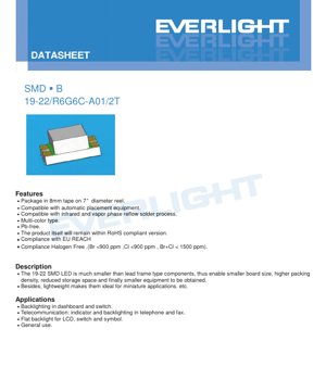
1. Product Overview
19-22 SMD LED wata ƙaramar na'ura ce mai hawa a saman, wacce aka tsara don aikace-aikacen PCB masu yawan girma. Wannan bambance-bambancen launi mai yawa ya haɗa ƙwayoyin LED guda biyu daban-daban a cikin fakit ɗaya: ɗaya yana fitar da Brilliant Red (R6) ɗayan kuma yana fitar da Brilliant Yellow Green (G6). Ƙaramin sawun sa yana ba da damar ajiye sarari sosai idan aka kwatanta da na'urorin da suka dace da gubar na gargajiya, wanda ke ba da gudummawa ga ƙananan ƙirar samfur na ƙarshe, rage buƙatun ajiya, da kuma yawan haɗawa mafi girma. Ƙirar sa mai sauƙi ya ƙara sa ya zama mai dacewa don na'urorin lantarki masu ɗaukuwa da ƙanana.
The product is engineered for compatibility with modern automated pick-and-place assembly lines and standard infrared or vapor phase reflow soldering processes. It adheres to stringent environmental and safety standards, being fully Pb-free, compliant with the EU RoHS directive, EU REACH regulations, and meeting halogen-free criteria (Br <900 ppm, Cl <900 ppm, Br+Cl < 1500 ppm).
2. Technical Parameter Deep-Dive
2.1 Absolute Maximum Ratings
These ratings define the stress limits beyond which permanent damage to the device may occur. Operation under or at these limits is not guaranteed and should be avoided for reliable long-term performance.
- Reverse Voltage (VR): 5 V. Exceeding this voltage in reverse bias can cause junction breakdown.
- Continuous Forward Current (IF): 25 mA for both R6 and G6 chips. This is the maximum DC current for continuous operation at Ta=25°C.
- Peak Forward Current (IFP): 60 mA (Duty 1/10 @1KHz). Suitable for pulsed operation but not for DC.
- Power Dissipation (Pd): 60 mW. The maximum power the package can dissipate, calculated as VF * IF.
- Electrostatic Discharge (ESD) HBM: 2000 V. Indicates the device's sensitivity; proper ESD handling procedures are mandatory.
- Operating Temperature (Topr): -40°C to +85°C. The ambient temperature range for normal operation.
- Storage Temperature (Tstg): -40°C to +90°C.
- Soldering Temperature: Reflow: 260°C peak for 10 seconds max. Hand soldering: 350°C for 3 seconds max per terminal.
2.2 Electro-Optical Characteristics (Ta=25°C)
These are the typical performance parameters measured under standard test conditions (IF=20mA, Ta=25°C).
- Luminous Intensity (Iv):
- R6 (Red): 45.0 - 112.0 mcd (see binning).
- G6 (Yellow Green): 45.0 - 72.0 mcd (see binning).
- Tolerance: ±11%.
- Viewing Angle (2θ1/2): 130° (typical). This wide angle ensures good visibility from various perspectives.
- Peak Wavelength (λp):
- R6: 632 nm (typical).
- G6: 575 nm (typical).
- Dominant Wavelength (λd):
- R6: 617.5 - 633.5 nm.
- G6: 567.5 - 575.5 nm.
- Tolerance: ±1 nm.
- Spectrum Radiation Bandwidth (Δλ): 20 nm (typical) for both colors, indicating relatively pure color emission.
- Forward Voltage (VF):
- R6 & G6: 1.7V (Min), 2.0V (Typ), 2.4V (Max) @ IF=20mA.
- Reverse Current (IR): 10 µA (Max) @ VR=5V.
3. Binning System Explanation
LEDs are sorted (binned) based on key optical parameters to ensure consistency within a production batch. This allows designers to select parts matching specific brightness and color requirements.
3.1 R6 (Brilliant Red) Binning
- Luminous Intensity Bins:
- P1: 45.0 - 57.0 mcd
- P2: 57.0 - 72.0 mcd
- Q1: 72.0 - 90.0 mcd
- Q2: 90.0 - 112.0 mcd
- Dominant Wavelength Bins:
- E4: 617.50 - 621.50 nm
- E5: 621.50 - 625.50 nm
- E6: 625.50 - 629.50 nm
- E7: 629.50 - 633.50 nm
3.2 G6 (Brilliant Yellow Green) Binning
- Luminous Intensity Bins:
- P1: 45.0 - 57.0 mcd
- P2: 57.0 - 72.0 mcd
- Dominant Wavelength Bins:
- C15: 567.50 - 569.50 nm
- C16: 569.50 - 571.50 nm
- C17: 571.50 - 573.50 nm
- C18: 573.50 - 575.50 nm
Cikakken lambar samfurin ya ƙunshi duka ƙa'idodin Intensity (CAT) da Wavelength (HUE), yana ba da damar zaɓi daidai.
4. Performance Curve Analysis
4.1 R6 Chip Characteristics
The provided curves for the R6 (Red) chip illustrate key relationships:
- Relative Luminous Intensity vs. Ambient Temperature: Luminous output decreases as ambient temperature increases, a typical behavior for LEDs due to reduced internal quantum efficiency and increased non-radiative recombination at higher temperatures.
- Forward Voltage vs. Forward Current (I-V Curve): Shows the exponential relationship. The curve's knee voltage is around 1.7-2.0V. The dynamic resistance can be inferred from the slope above the knee voltage.
- Relative Luminous Intensity vs. Forward Current: Output is roughly linear with current in the normal operating range (up to ~20-30mA), after which efficiency may drop due to heating and other effects.
- Spectrum Distribution: The graph shows a dominant peak around 632 nm (red) with a typical full width at half maximum (FWHM) of approximately 20 nm.
4.2 G6 Chip Characteristics
Similar curves are provided for the G6 (Yellow Green) chip, depicting:
- Relative Luminous Intensity vs. Ambient Temperature.
- Forward Voltage vs. Forward Current.
- Relative Luminous Intensity vs. Forward Current.
- Spectrum Distribution: Expected peak around 575 nm.
These curves are essential for thermal management design and for predicting performance under non-standard operating conditions.
5. Mechanical & Package Information
5.1 Package Dimensions
The 19-22 SMD LED has a very compact footprint. Key dimensions (tolerance ±0.1mm unless noted) include:
- Package Length: 2.0 mm
- Package Width: 1.25 mm
- Package Height: 0.8 mm
- Terminal dimensions and spacing are defined for reliable soldering.
The detailed dimensioned drawing is crucial for PCB land pattern design (footprint). A correctly designed footprint ensures proper solder joint formation, alignment, and mechanical stability.
5.2 Polarity Identification
The package includes a polarity indicator, typically a notch or a marked cathode. Correct orientation during placement is vital for circuit functionality.
6. Soldering & Assembly Guidelines
6.1 Reflow Soldering Profile (Pb-free)
A critical process for reliable assembly. The recommended profile includes:
- Pre-heating: 150-200°C for 60-120 seconds. Gradual heating to minimize thermal shock.
- Time Above Liquidus (TAL): 60-150 sekunde sama 217°C.
- Peak Temperature: Maximum 260°C, an riƙe na maximum 10 seconds.
- Heating Rate: Maximum 6°C/second up to 255°C.
- Cooling Rate: Maximum 3°C/second.
- Reflow Limit: The assembly should not undergo reflow soldering more than two times to prevent excessive thermal stress on the LED package and wire bonds.
6.2 Hand Soldering
If manual soldering is necessary:
- Iron tip temperature: < 350°C.
- Lokacin tuntuɓar kowane tasha: ≤ daƙiƙa 3.
- Ƙarfin guntun walda: ≤ 25W.
- A guji amfani da matsi na inji akan kayan aikin yayin ko bayan walda.
6.3 Storage & Moisture Sensitivity
The LEDs are packaged in a moisture-resistant barrier bag with desiccant to prevent moisture absorption, which can cause "popcorning" (package cracking) during reflow.
- Kafin Amfani: Kada a buɗe jakar kariyar ɗanɗano har sai an shirya don haɗawa.
- Bayan Buɗewa: Use within 168 hours (7 days) if stored at ≤ 30°C and ≤ 60% RH.
- Rebaking: If the exposure time is exceeded or desiccant is saturated, bake at 60 ±5°C for 24 hours before use.
7. Packaging & Ordering Information
7.1 Tape and Reel Specifications
The components are supplied in industry-standard embossed carrier tape for automated assembly.
- Carrier Tape Width: 8 mm.
- Reel Diameter: 7 inches.
- Pocket Pitch: Defined in the carrier tape drawing.
- Quantity per Reel: 2000 pieces.
Detailed reel and tape dimensions are provided for compatibility with feeder equipment.
7.2 Label Explanation
The reel label contains several codes essential for traceability and verification:
- P/N: Product Number (e.g., 19-22/R6G6C-A01/2T).
- QTY: Packing Quantity.
- CAT: Luminous Intensity Rank (Bin Code).
- HUE: Chromaticity Coordinates & Dominant Wavelength Rank (Bin Code).
- REF: Forward Voltage Rank.
- LOT No: Manufacturing Lot Number for traceability.
8. Application Suggestions
8.1 Typical Application Scenarios
- Backlighting: Ideal for dashboard indicators, switch backlighting, and flat backlighting for LCD symbols due to their small size and good brightness.
- Status Indicators: Perfect for telecommunication equipment (phones, fax machines), consumer electronics, and industrial control panels as multi-color status or function indicators.
- General Purpose Indication: Any application requiring compact, reliable, and bright visual indicators.
8.2 Design Considerations
- Current Limiting: An external current-limiting resistor is absolutely mandatory. LED's exponential I-V characteristic means a small increase in voltage causes a large current increase, leading to instantaneous failure. The resistor value is calculated as R = (Vsupply - VF) / IF.
- Thermal Management: While power dissipation is low, maintaining the junction temperature within limits is key for longevity and stable light output. Ensure adequate PCB copper area or thermal vias if operating at high ambient temperatures or currents.
- ESD Protection: Implement ESD protection on input lines if the LED is exposed to user interfaces, and always follow ESD-safe handling procedures during assembly.
- PCB Layout: Follow the recommended land pattern from the dimension drawing. Ensure solder mask dams between pads to prevent bridging.
9. Technical Comparison & Differentiation
The 19-22 series offers distinct advantages in specific contexts:
- vs. Larger SMD LEDs (e.g., 3528, 5050): The primary advantage is the significantly smaller footprint (2.0x1.25mm), enabling ultra-miniaturized designs where board space is at a premium. The trade-off is generally lower total light output per package.
- vs. Single-Color 19-22 LEDs: This specific A01/2T variant integrates two different color chips (Red and Yellow-Green) in one package. This saves space and placement cost compared to using two separate single-color LEDs, simplifying designs requiring dual-color indication.
- vs. Through-Hole LEDs: Offers all standard SMD benefits: suitability for automated assembly, no lead bending/trimming, lower profile, and better performance in high-vibration environments.
- Compliance: Its full suite of compliance (Pb-free, RoHS, REACH, Halogen-Free) makes it suitable for the most demanding global markets and environmentally conscious designs.
10. Frequently Asked Questions (Based on Technical Parameters)
Q1: Can I drive this LED directly from a 3.3V or 5V logic supply without a resistor?
A: No, never. You must use a series current-limiting resistor. Without it, the forward voltage is only ~2.0V, so the excess voltage from a 3.3V or 5V supply will cause excessive current, destroying the LED instantly.
Q2: What is the difference between Peak Wavelength and Dominant Wavelength?
A: Peak Wavelength (λp) is the wavelength at which the emission spectrum has its maximum intensity. Dominant Wavelength (λd) is the single wavelength of monochromatic light that matches the perceived color of the LED. λd is more relevant for color specification. The datasheet provides both.p) is the wavelength at which the emission spectrum has its maximum intensity. Dominant Wavelength (λd) is the single wavelength of monochromatic light that matches the perceived color of the LED. λd is more relevant for color specification. The datasheet provides both.
Q3: How do I select the correct bin codes for my application?
A: Idan ƙirarku tana buƙatar daidaiton haske a cikin raka'a da yawa, ƙayyade ƙaƙƙarfan rukunin ƙarfin haske (misali, P2 kawai). Idan daidaiton launi yana da mahimmanci (misali, don daidaita launi), ƙayyade ƙunƙun tsayin tsayin raƙuman ruwa (misali, E5 don ja). Dubi teburin binning a sashe na 3.1 da 3.2.
Q4: Yanayin aiki ya kai 85°C. Zan iya amfani da shi a aikace-aikacen waje?
A: Ƙimar 85°C tana nufin yanayin iska da ke kewaye da na'urar. A cikin akwati na waje da ke fuskantar hasken rana kai tsaye, yanayin ciki zai iya wuce wannan cikin sauƙi. Dole ne ku ƙirƙira tsarin don tabbatar da yanayin yanayin gida na LED ya kasance cikin -40°C zuwa +85°C, la'akari da dumamar rana, zafi na ciki daga wasu sassa, da rashin iska.
Q5: A cikin dalilin da ya sa akwai tsayayyen rayuwar bene na kwanaki 7 bayan bude jakar shinge na danshi?
A: Kunshin LED na filastik na iya ɗaukar danshi daga iska. A lokacin tsarin haɗa sake kwarara mai zafi, wannan danshin da ke ciki ya zama tururi cikin sauri, yana haifar da matsin lamba wanda zai iya raba kunshin ko fashe siminti, gazawar da aka sani da "popcorning." Iyakar kwanaki 7 tana ɗaukar yanayin ajiya daidai (30°C/60%RH).
11. Practical Design & Usage Case Study
Scenario: Designing a Dual-Color Status Indicator for a Portable Medical Device.
Requirements: The device needs a single, tiny indicator to show "Standby" (Green) and "Fault" (Red). Board space is extremely limited. The device must be RoHS and halogen-free for global medical market compliance.
Component Selection: The 19-22/R6G6C-A01/2T is an ideal candidate. Its 2.0x1.25mm footprint saves crucial space. The integrated Red (R6) and Yellow-Green (G6) chips eliminate the need for two separate LEDs and their associated placement cycles. Its full environmental compliance meets regulatory needs.
Circuit Design: An kera biyu masu zaman kansu an tsara su, kowanne ya ƙunshi filin GPIO daga microcontroller, resistor mai iyakancewar ƙarfin lantarki, da kuma anode mai dacewa na fakitin LED. An haɗa cathode gama gari zuwa ƙasa. An lissafta ƙimar resistor don manufar ƙarfin lantarki na 15mA (ƙasa da 25mA matsakaicin) don tsawon rayuwa: R = (3.3V - 2.0V) / 0.015A ≈ 87Ω (yi amfani da ƙimar daidaitaccen 82Ω ko 100Ω).
PCB Layout: An yi amfani da tsarin ƙasa da aka ba da shawarar daga takardar bayanan. An yi amfani da ƙananan haɗin thermal relief akan ɓangarorin don sauƙaƙe soldering yayin kiyaye kyakkyawar haɗin thermal zuwa ƙaramin zubar da ƙasa don zubar da zafi.
Assembly & Result: The parts are supplied on 8mm tape for automatic placement. The designed reflow profile is followed precisely. The final product has a clean, professional-looking dual-color indicator that meets all size, reliability, and compliance requirements.
12. Technology Introduction
The 19-22 LED utilizes AlGaInP (Aluminum Gallium Indium Phosphide) semiconductor material for both the R6 (Red) and G6 (Yellow-Green) chips. AlGaInP is a direct bandgap III-V compound semiconductor well-suited for producing high-efficiency light emission in the amber-to-red color spectrum (approximately 560-650 nm). By carefully adjusting the ratios of Aluminum, Gallium, and Indium in the crystal lattice, the bandgap energy—and thus the emitted photon wavelength—can be precisely tuned.
The basic operating principle is electroluminescence. When a forward voltage is applied across the p-n junction, electrons from the n-type region and holes from the p-type region are injected into the active region. There, they recombine radiatively, releasing energy in the form of photons. The wavelength (color) of these photons is determined by the bandgap energy of the semiconductor material in the active region. The chip is encapsulated in a clear epoxy resin which protects the semiconductor die, acts as a lens to shape the light output (achieving the 130° viewing angle), and provides mechanical stability.
13. Technology Trends
The market for miniature SMD LEDs like the 19-22 continues to evolve driven by several key trends:
- Increased Miniaturization: The demand for ever-smaller consumer electronics, wearables, and medical devices pushes for LEDs with smaller footprints and lower profiles than the 19-22, such as chip-scale package (CSP) LEDs or even smaller package types.
- Higher Efficiency & Luminance: Ongoing improvements in epitaxial growth, chip design, and package extraction efficiency lead to higher luminous intensity from the same or smaller chip sizes, allowing designers to use less current for the same brightness, improving battery life and thermal performance.
- Advanced Color Options & Multi-Chip Integration: The trend exemplified by this product—integrating multiple colors—is expanding to include RGB (Red-Green-Blue) or RGBW (Red-Green-Blue-White) in tiny packages, enabling full-color programmability in a single point source.
- Enhanced Reliability & Harsh Environment Suitability: Developments in encapsulation materials (e.g., silicones instead of epoxy for better heat and UV resistance) and package structures are improving LED lifetime and performance in automotive, industrial, and outdoor applications.
- Intelligent Integration: A broader trend involves integrating control circuitry (like constant current drivers or simple logic) directly with the LED die or within the package, moving towards "smart LED" components that simplify system design.
The 19-22 series represents a mature, reliable solution in this landscape, particularly suited for cost-effective, space-constrained indicator applications requiring robust performance and broad compliance.
LED Specification Terminology
Complete explanation of LED technical terms
Photoelectric Performance
| Term | Unit/Representation | Simple Explanation | Why Important |
|---|---|---|---|
| Luminous Efficacy | lm/W (lumens per watt) | Haske a kowane watt na wutar lantarki, mafi girma yana nufin mafi ingancin makamashi. | Yana ƙayyadaddun matakin ingancin makamashi da farashin wutar lantarki kai tsaye. |
| Luminous Flux | lm (lumens) | Total light emitted by source, commonly called "brightness". | Determines if the light is bright enough. |
| Viewing Angle | ° (degrees), e.g., 120° | Angle where light intensity drops to half, determines beam width. | Affects illumination range and uniformity. |
| CCT (Color Temperature) | K (Kelvin), e.g., 2700K/6500K | Mwangaza wa joto/baridi, thamani za chini ni manjano/joto, za juu nyeupe/baridi. | Huamua mazingira ya taa na matukio yanayofaa. |
| CRI / Ra | Unitless, 0–100 | Ability to render object colors accurately, Ra≥80 is good. | Affects color authenticity, used in high-demand places like malls, museums. |
| SDCM | MacAdam ellipse steps, e.g., "5-step" | Color consistency metric, smaller steps mean more consistent color. | Ensures uniform color across same batch of LEDs. |
| Dominant Wavelength | nm (nanometers), e.g., 620nm (red) | Wavelength corresponding to color of colored LEDs. | Determines hue of red, yellow, green monochrome LEDs. |
| Spectral Distribution | Wavelength vs intensity curve | Shows intensity distribution across wavelengths. | Affects color rendering and quality. |
Electrical Parameters
| Term | Symbol | Simple Explanation | Design Considerations |
|---|---|---|---|
| Forward Voltage | Vf | Minimum voltage to turn on LED, like "starting threshold". | Driver voltage must be ≥Vf, voltages add up for series LEDs. |
| Forward Current | If | Current value for normal LED operation. | Usually constant current drive, current determines brightness & lifespan. |
| Max Pulse Current | Ifp | Peak current tolerable for short periods, used for dimming or flashing. | Pulse width & duty cycle must be strictly controlled to avoid damage. |
| Reverse Voltage | Vr | Max reverse voltage LED can withstand, beyond may cause breakdown. | Circuit must prevent reverse connection or voltage spikes. |
| Thermal Resistance | Rth (°C/W) | Resistance to heat transfer from chip to solder, lower is better. | High thermal resistance requires stronger heat dissipation. |
| ESD Immunity | V (HBM), e.g., 1000V | Ability to withstand electrostatic discharge, higher means less vulnerable. | Anti-static measures needed in production, especially for sensitive LEDs. |
Thermal Management & Reliability
| Term | Key Metric | Simple Explanation | Impact |
|---|---|---|---|
| Junction Temperature | Tj (°C) | Yanzu aiki zazzabi a cikin LED chip. | Kowane raguwar 10°C na iya ninka tsawon rayuwa; yana da yawa yana haifar da lalacewar haske, canjin launi. |
| Lumen Depreciation | L70 / L80 (hours) | Time for brightness to drop to 70% or 80% of initial. | Directly defines LED "service life". |
| Lumen Maintenance | % (e.g., 70%) | Percentage of brightness retained after time. | Indicates brightness retention over long-term use. |
| Color Shift | Δu′v′ or MacAdam ellipse | Ihe mgbanwe agba n'oge ojiji. | Na-emetụta nkwụsi ike agba na ihe ngosi ọkụ. |
| Thermal Aging | Material degradation | Deterioration due to long-term high temperature. | May cause brightness drop, color change, or open-circuit failure. |
Packaging & Materials
| Term | Common Types | Simple Explanation | Features & Applications |
|---|---|---|---|
| Package Type | EMC, PPA, Ceramic | Housing material protecting chip, providing optical/thermal interface. | EMC: good heat resistance, low cost; Ceramic: better heat dissipation, longer life. |
| Usoro Chip | Ihu, Flip Chip | Chip electrode arrangement. | Flip chip: better heat dissipation, higher efficacy, for high-power. |
| Phosphor Coating | YAG, Silicate, Nitride | Covers blue chip, converts some to yellow/red, mixes to white. | Phosphors ya daban-daban suna tasiri aikin haske, zafin launi (CCT), da ma'aunin launi (CRI). |
| Ruwan tabarau/Optics | Flat, Microlens, TIR | Optical structure on surface controlling light distribution. | Determines viewing angle and light distribution curve. |
Quality Control & Binning
| Term | Binning Content | Simple Explanation | Purpose |
|---|---|---|---|
| Luminous Flux Bin | Code e.g., 2G, 2H | Grouped by brightness, each group has min/max lumen values. | Ensures uniform brightness in same batch. |
| Voltage Bin | Code e.g., 6W, 6X | Grouped by forward voltage range. | Yana taimaka da daidaita direbobi, yana inganta ingancin tsarin. |
| Kwandon Launi | 5-step MacAdam ellipse | Grouped by color coordinates, ensuring tight range. | Guarantees color consistency, avoids uneven color within fixture. |
| CCT Bin | 2700K, 3000K etc. | Grouped by CCT, each has corresponding coordinate range. | Meets different scene CCT requirements. |
Testing & Certification
| Term | Standard/Test | Simple Explanation | Significance |
|---|---|---|---|
| LM-80 | Lumen maintenance test | Long-term lighting at constant temperature, recording brightness decay. | Used to estimate LED life (with TM-21). |
| TM-21 | Life estimation standard | Inakadiria maisha chini ya hali halisi kulingana na data ya LM-80. | Inatoa utabiri wa kisayansi wa maisha. |
| IESNA | Illuminating Engineering Society | Covers optical, electrical, thermal test methods. | Industry-recognized test basis. |
| RoHS / REACH | Environmental certification | Ensures no harmful substances (lead, mercury). | Market access requirement internationally. |
| ENERGY STAR / DLC | Energy efficiency certification | Energy efficiency and performance certification for lighting. | Used in government procurement, subsidy programs, enhances competitiveness. |