Table of Contents
- 1. Product Overview
- 2. Technical Parameter Deep-Dive
- 2.1 Absolute Maximum Ratings
- 2.2 Electro-Optical Characteristics
- 3. Binning System Explanation
- 3.1 Luminous Intensity Binning
- 3.2 Dominant Wavelength Binning
- 3.3 Forward Voltage Binning
- 4. Performance Curve Analysis
- 5. Mechanical and Package Information
- 6. Soldering and Assembly Guidelines
- 6.1 Storage and Handling
- 6.2 Reflow Soldering Process
- 6.3 Hand Soldering and Rework
- 7. Packaging and Ordering Information
- 8. Application Notes and Design Considerations
- 8.1 Typical Applications
- 8.2 Critical Design Considerations
- 8.3 Application Restrictions
- 9. Technical Comparison and Positioning
- 10. Frequently Asked Questions (FAQ)
- 10.1 How do I select the correct current-limiting resistor?
- 10.2 Shin zan iya kunna wannan LED ba tare da resistor ta amfani da tushen ƙarfin lantarki mai tsayayye ba?
- 10.3 Me ya sa akwai iyakar kwanaki 7 bayan buɗe jakar kariya daga danshi?
- 10.4 What do the bin codes (e.g., S2/A11/6) mean for my design?
- 11. Practical Design Example
- 12. Operating Principle
- 13. Technology Trends
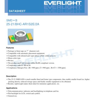
1. Product Overview
The 25-21/BHC-AR1S2E/2A is a surface-mount device (SMD) light-emitting diode (LED) utilizing an InGaN (Indium Gallium Nitride) semiconductor chip to produce blue light. This component belongs to a class of LEDs designed for high-density board assembly, offering significant advantages in miniaturization and automated production processes.
The core advantage of this LED is its compact footprint. With dimensions of approximately 2.5mm x 2.1mm, it enables smaller printed circuit board (PCB) designs, higher component packing density, and ultimately contributes to the development of smaller end-user equipment. Its lightweight construction further makes it ideal for applications where space and weight are critical constraints.
This is a mono-color (blue) type LED. The device is constructed with lead-free (Pb-free) materials and complies with major environmental regulations including the EU RoHS (Restriction of Hazardous Substances) directive and REACH (Registration, Evaluation, Authorisation and Restriction of Chemicals). It is also classified as halogen-free, with bromine (Br) and chlorine (Cl) content kept below specified limits (Br <900 ppm, Cl <900 ppm, Br+Cl < 1500 ppm). The product is supplied in a format compatible with modern manufacturing, packaged on 8mm tape wound onto a 7-inch diameter reel, suitable for use with automatic pick-and-place equipment.
2. Technical Parameter Deep-Dive
Wannan sashe yana ba da cikakken bincike na haƙiƙa na mahimman sigogi na lantarki, na gani, da na zafi waɗanda aka ayyana a cikin takardar bayanai. Fahimtar waɗannan iyakoki da ƙimar yau da kullun yana da mahimmanci ga ingantaccen ƙira na kewaye.
2.1 Absolute Maximum Ratings
The Absolute Maximum Ratings define the stress limits beyond which permanent damage to the device may occur. These are not conditions for normal operation.
- Reverse Voltage (VR): 5V Applying a reverse bias voltage exceeding 5V can cause junction breakdown.
- Continuous Forward Current (IF): 20mA This is the maximum DC current recommended for continuous operation to ensure long-term reliability and maintain specified optical performance.
- Peak Forward Current (IFP): 100mA This rating allows for pulsed operation (duty cycle 1/10 at 1kHz). It is useful for applications requiring brief bursts of higher brightness but must not be exceeded even momentarily.
- Power Dissipation (Pd): 75mW This is the maximum amount of power the package can dissipate as heat (calculated as Forward Voltage x Forward Current) at an ambient temperature (Ta) of 25°C. Exceeding this limit risks overheating.
- Operating & Storage Temperature: The device can function in ambient temperatures from -40°C to +85°C and can be stored in temperatures from -40°C to +90°C.
- Electrostatic Discharge (ESD): The Human Body Model (HBM) rating is 150V. This indicates a moderate sensitivity to ESD, necessitating standard ESD precautions during handling.
- Soldering Temperature: The package can withstand reflow soldering with a peak temperature of 260°C for up to 10 seconds, or hand soldering at 350°C for up to 3 seconds per terminal.
2.2 Electro-Optical Characteristics
These parameters are measured under standard test conditions (Ta=25°C, IF=20mA) and define the device's performance.
- Luminous Intensity (Iv): Ranges from a minimum of 112 millicandelas (mcd) to a maximum of 285 mcd. The wide range is managed through a binning system (detailed later). The typical value is not specified, falling somewhere within this bin range.
- Viewing Angle (2θ1/2): The full angle at which luminous intensity drops to half of its peak value is typically 60 degrees. This defines the beam spread of the LED.
- Peak Wavelength (λp): The wavelength at which the optical power output is maximum is typically 468 nanometers (nm), placing it in the blue region of the visible spectrum.
- Dominant Wavelength (λd): This is the single wavelength perceived by the human eye, ranging from 464.5 nm to 476.5 nm. It is also subject to binning.
- Spectral Bandwidth (Δλ): Typically 25 nm, this indicates the spread of wavelengths emitted around the peak wavelength.
- Forward Voltage (VF): Ranges from 2.75V to 3.65V when driven at 20mA. This variation is managed by a voltage binning system. A current-limiting resistor must be used in series with the LED to control the current based on the actual VF of the specific unit and the supply voltage.
- Reverse Current (IR): Maximum of 50 microamperes (μA) when a 5V reverse bias is applied.
3. Binning System Explanation
To ensure consistency in mass production, LEDs are sorted (binned) based on key performance parameters. This allows designers to select parts that meet specific requirements for brightness, color, and voltage.
3.1 Luminous Intensity Binning
LEDs are categorized into four bins (R1, R2, S1, S2) based on their measured luminous intensity at 20mA.
- Bin R1: 112 mcd to 140 mcd
- Bin R2: 140 mcd to 180 mcd
- Bin S1: 180 mcd to 225 mcd
- Bin S2: 225 mcd to 285 mcd
A tolerance of ±11% applies to the luminous intensity within each bin code.
3.2 Dominant Wavelength Binning
LEDs are sorted into four bins (A9, A10, A11, A12) to control the shade of blue.
- Bin A9: 464.5 nm to 467.5 nm
- Bin A10: 467.5 nm to 470.5 nm
- Bin A11: 470.5 nm to 473.5 nm
- Bin A12: 473.5 nm to 476.5 nm
A tolerance of ±1nm applies to the dominant wavelength within each bin code.
3.3 Forward Voltage Binning
LEDs are grouped into three voltage bins (5, 6, 7) to aid in current regulation circuit design.
- Bin 5: 2.75V to 3.05V
- Bin 6: 3.05V to 3.35V
- Bin 7: 3.35V to 3.65V
A tolerance of ±0.1V applies to the forward voltage within each bin code.
4. Performance Curve Analysis
While the datasheet references typical electro-optical characteristic curves, the provided text does not include the specific graphs. Based on standard LED behavior, these curves would typically illustrate the following relationships, which are critical for design:
- I-V (Current-Voltage) Curve: Inaonyesha uhusiano wa kielelezo kati ya voltage ya mbele na mkondo. Voltage ya goti ya mkunjo inahusiana na vipimo vya VF. Grafu hii ni muhimu kwa kuchagua thamani inayofaa ya kipingamizi cha kudhibiti mkondo.
- Luminous Intensity vs. Forward Current: Yana nuna yadda haske ke ƙaruwa tare da ƙarfin tuƙi, yawanci a cikin alaƙar kusa da layi har zuwa wani lokaci, bayan haka inganci ya ragu.
- Ƙarfin Haske da Yanayin Yanayi: Yana nuna raguwar fitar da haske yayin da zafin haɗin gwiwa ya tashi. Wannan yana da mahimmanci ga aikace-aikacen da ke aiki a cikin yanayin zafi mai girma.
- Rarraba Bakan: A plot of relative intensity versus wavelength, showing the peak at ~468nm and the 25nm bandwidth, confirming the blue color purity.
5. Mechanical and Package Information
The LED is housed in a plastic surface-mount package. The datasheet includes a detailed dimensioned drawing. Key mechanical features include:
- Tsarin Fakitin: Matsakaicin girma na jiki shine kusan 2.5mm tsayi da 2.1mm faɗi. Zanen ya ƙayyade duk mahimman ma'auni ciki har da girman jagora (tasha), tazara, da tsayin fakitin tare da daidaitaccen jurewar ±0.1mm sai dai idan an faɗi akasin haka.
- Gano Ƙaddara: The cathode terminal is typically marked, often by a notch, a dot, or a green marking on the package itself, as indicated in the drawing. Correct polarity is essential for operation.
- Pad Design (Footprint): The recommended PCB land pattern (pad size and shape) is derived from the package dimensions to ensure reliable soldering and mechanical stability.
6. Soldering and Assembly Guidelines
Adherence to these guidelines is critical to prevent damage during the assembly process.
6.1 Storage and Handling
- The LEDs are packaged in a moisture-resistant bag with desiccant.
- Do not open the moisture-proof bag until the components are ready for use.
- After opening, unused LEDs must be stored at ≤30°C and ≤60% relative humidity.
- The floor life After opening the bag is 168 hours (7 days). If not used within this time, they must be re-baked and re-bagged.
- Baking Condition: If required, bake at 60 ±5°C for 24 hours.
- Always observe ESD (Electrostatic Discharge) precautions during handling.
6.2 Reflow Soldering Process
A detailed temperature profile for lead-free (Pb-free) reflow soldering is provided:
- Pre-heating: Ramp from 150°C to 200°C over 60-120 seconds.
- Soak/Reflow: Time above 217°C (liquidus temperature) should be 60-150 seconds. The peak temperature must not exceed 260°C, and the time at or above 255°C must be limited to a maximum of 30 seconds.
- Cooling Rate: Maximum cooling rate is 6°C per second.
- Important: Reflow soldering should not be performed more than two timesAvoid mechanical stress on the LED during heating and do not warp the PCB after soldering.
6.3 Hand Soldering and Rework
- If hand soldering is necessary, use a soldering iron with a tip temperature ≤350°C for ≤3 seconds per terminal.
- The iron power should be ≤25W. Allow a cooling interval of at least 2 seconds between soldering each terminal.
- Repair/Rework is strongly discouraged after the LED is soldered. If unavoidable, a specialized double-head soldering iron must be used to simultaneously heat both terminals and lift the component without stressing the solder joints. The impact on LED characteristics must be verified beforehand.
7. Packaging and Ordering Information
The product is supplied for automated assembly.
- Carrier Tape: Components are loaded into embossed carrier tape with a width of 8mm.
- Reel: The tape is wound onto a standard 7-inch (178mm) diameter reel.
- Quantity: Each reel contains 2000 pieces of the LED.
- Moisture Barrier Bag: The reel is sealed inside an aluminum moisture-proof bag with a desiccant and a humidity indicator card.
- Label Information: The reel label contains codes for the product number (P/N), quantity (QTY), and the specific bin codes for Luminous Intensity (CAT), Dominant Wavelength (HUE), and Forward Voltage (REF), along with a lot number (LOT No).
8. Application Notes and Design Considerations
8.1 Typical Applications
Based on its specifications, this blue SMD LED is suitable for a variety of low-power indicator and backlighting functions, including:
- Telecommunication Equipment: Status indicators, backlighting for keys or displays in telephones and fax machines.
- Consumer Electronics: Switch and symbol illumination, flat backlighting for small liquid crystal displays (LCDs).
- General Purpose Indication: Any application requiring a compact, reliable, blue status light.
8.2 Critical Design Considerations
- Current Limiting is Mandatory: An LED is a current-driven device. You must use a series resistor (or a constant current driver) to limit the forward current to 20mA or less. The resistor value is calculated as R = (V_supply - VF_LED) / I_desired. Using the maximum VF (3.65V) for this calculation ensures the current never exceeds the limit even with a low-supply-voltage unit.
- Thermal Management: While the power is low (75mW max), ensuring adequate PCB copper area or thermal vias around the LED pads can help dissipate heat, especially in high ambient temperature conditions, maintaining light output and longevity.
- Optical Design: The 60-degree viewing angle provides a fairly wide beam. For more focused light, external lenses or reflectors may be required.
8.3 Application Restrictions
The datasheet explicitly states that this product is not designed or qualified for high-reliability applications where failure could lead to serious consequences. This includes:
- Military and aerospace systems
- Automotive safety and security systems (e.g., airbags, braking)
- Medical life-support or critical diagnostic equipment
For such applications, components with different specifications, qualifications, and reliability assurances are required.
9. Technical Comparison and Positioning
The 25-21 package sits between smaller chips like 0402/0603 and larger power LEDs. Its key differentiators are:
- vs. Smaller Packages (e.g., 0402): Offers higher light output and is generally easier to handle and solder manually if needed, while still being very compact.
- vs. Leaded LEDs: Enables fully automated assembly, reduces board space, and eliminates the need for lead bending and through-hole drilling.
- vs. High-Power LEDs: Designed for indicator-level currents (20mA) and power (75mW), not for illumination. It requires simple drive circuitry (a resistor) compared to the complex constant-current drivers needed for high-power LEDs.
10. Frequently Asked Questions (FAQ)
10.1 How do I select the correct current-limiting resistor?
Yi amfani da dabara: R = (V_supply - VF) / I_desired. Don wadata na 5V da kuma halin yanzu da ake so na 20mA, kuma a ɗauka mafi munin yanayi (mafi girma) VF na 3.65V: R = (5V - 3.65V) / 0.020A = 67.5 Ohms. Yi amfani da ƙimar da ta biyo baya mafi girma (misali, 68 Ohms ko 75 Ohms). Wannan yana tabbatar da cewa halin yanzu ya kasance ƙasa da 20mA ga dukkan raka'a. Koyaushe a lissafta ɓarnawar wutar lantarki a cikin resistor: P_resistor = I^2 * R.
10.2 Shin zan iya kunna wannan LED ba tare da resistor ta amfani da tushen ƙarfin lantarki mai tsayayye ba?
No. The forward voltage of an LED has a negative temperature coefficient and varies from unit to unit. Connecting it directly to a voltage source even slightly above its VF will cause current to rise uncontrollably, potentially exceeding the Absolute Maximum Rating and destroying the LED almost instantly.
10.3 Me ya sa akwai iyakar kwanaki 7 bayan buɗe jakar kariya daga danshi?
SMD plastic packages can absorb moisture from the air. During the high-temperature reflow soldering process, this trapped moisture can rapidly expand, causing internal delamination or "popcorning" that cracks the package or damages the die. The 7-day floor life and baking procedures are designed to remove this absorbed moisture before soldering.
10.4 What do the bin codes (e.g., S2/A11/6) mean for my design?
They specify the performance group of your specific LEDs. If your design requires minimum brightness, you should specify a bin like S1 or S2. If color consistency across multiple LEDs is critical, you should specify a tight wavelength bin (e.g., A10 only). Specifying a voltage bin (e.g., 5) can help make the current (and thus brightness) more consistent across units when using a simple resistor drive.
11. Practical Design Example
Scenario: Design a simple blue power indicator for a device running on a 3.3V rail. We want approximately 15mA of current for adequate brightness while being conservative.
- Determine Worst-Case VF: From the datasheet, maximum VF (Bin 7) is 3.65V.
- Calculate Minimum Resistor Value: R_min = (V_supply - VF_max) / I_desired = (3.3V - 3.65V) / 0.015A = -23.3 Ohms. This is negative, meaning with a 3.3V supply and a unit with VF=3.65V, no current would flow. This is acceptable; the LED simply won't turn on for that specific high-VF unit at this low supply voltage.
- Calculate for Typical/Low VF: Let's use a typical VF of 3.2V. R = (3.3V - 3.2V) / 0.015A ≈ 6.7 Ohms. Using a 10 Ohm standard resistor: I_actual = (3.3V - 3.2V) / 10 = 10mA (safe). For a low VF unit of 2.8V: I = (3.3V - 2.8V) / 10 = 50mA. This exceeds the 20mA continuous rating!
- Conclusion: A 3.3V supply is too close to the LED's forward voltage range for reliable, safe operation with just a series resistor. The current will vary wildly (from 0mA to over 50mA) depending on the individual LED's VF. A better solution is to use a higher supply voltage (e.g., 5V) or a dedicated low-dropout constant current driver IC designed for low-voltage operation.
12. Operating Principle
This LED operates on the principle of electroluminescence in a semiconductor p-n junction. The active region uses an InGaN (Indium Gallium Nitride) compound semiconductor. When a forward bias voltage exceeding the junction's built-in potential is applied, electrons from the n-type region and holes from the p-type region are injected into the active region. There, they recombine, releasing energy in the form of photons (light). The specific composition of the InGaN alloy determines the bandgap energy, which directly corresponds to the wavelength (color) of the emitted light—in this case, blue (~468 nm). The epoxy resin encapsulant protects the semiconductor chip, acts as a lens to shape the light output, and is formulated to be water-clear to maximize light transmission.
13. Technology Trends
SMD LEDs in packages like the 25-21 represent a mature and widely adopted technology. Current trends in this segment focus on several key areas:
- Increased Efficiency: Ongoing material science and epitaxial growth improvements aim to produce more light (higher luminous efficacy) per unit of electrical input power (mA), allowing for lower power consumption or higher brightness at the same current.
- Improved Color Consistency: Advances in manufacturing control and binning algorithms lead to tighter distributions in dominant wavelength and luminous intensity, reducing the need for extensive binning and providing more uniform appearance in multi-LED applications.
- Enhanced Reliability: Research into more robust package materials, better die attach methods, and improved phosphors (for white LEDs) continues to extend operational lifetime and stability under various environmental stresses.
- Miniaturization Continuation: While the 25-21 is small, the drive for even smaller form factors (e.g., chip-scale packages) persists for ultra-compact devices, though often with trade-offs in ease of handling and thermal performance.
- Integration: A broader trend involves integrating control electronics (like constant current drivers or pulse-width modulation circuits) directly with the LED die into a single package, simplifying end-user circuit design.
LED Specification Terminology
Complete explanation of LED technical terms
Photoelectric Performance
| Term | Unit/Representation | Simple Explanation | Why Important |
|---|---|---|---|
| Luminous Efficacy | lm/W (lumens per watt) | Light output per watt of electricity, higher means more energy efficient. | Directly determines energy efficiency grade and electricity cost. |
| Luminous Flux | lm (lumens) | Total light emitted by source, commonly called "brightness". | Determines if the light is bright enough. |
| Viewing Angle | ° (degrees), e.g., 120° | Kwanin da ƙarfin haske ya ragu zuwa rabi, yana ƙayyade faɗin katako. | Yana shafar kewayon haskakawa da daidaito. |
| CCT (Color Temperature) | K (Kelvin), e.g., 2700K/6500K | Warmth/coolness of light, lower values yellowish/warm, higher whitish/cool. | Determines lighting atmosphere and suitable scenarios. |
| CRI / Ra | Unitless, 0–100 | Ability to render object colors accurately, Ra≥80 is good. | Affects color authenticity, used in high-demand places like malls, museums. |
| SDCM | MacAdam ellipse steps, e.g., "5-step" | Metric ya Consistency ya Rangi, hatua ndogo zina maana rangi inaendana zaidi. | Inahakikisha rangi sawa kwenye kundi moja la LEDs. |
| Dominant Wavelength | nm (nanometers), e.g., 620nm (red) | Wavelength corresponding to color of colored LEDs. | Determines hue of red, yellow, green monochrome LEDs. |
| Spectral Distribution | Wavelength vs intensity curve | Shows intensity distribution across wavelengths. | Affects color rendering and quality. |
Electrical Parameters
| Term | Symbol | Simple Explanation | Design Considerations |
|---|---|---|---|
| Forward Voltage | Vf | Minimum voltage to turn on LED, like "starting threshold". | Driver voltage must be ≥Vf, voltages add up for series LEDs. |
| Forward Current | If | Current value for normal LED operation. | Usually constant current drive, current determines brightness & lifespan. |
| Max Pulse Current | Ifp | Peak current tolerable for short periods, used for dimming or flashing. | Pulse width & duty cycle must be strictly controlled to avoid damage. |
| Reverse Voltage | Vr | Max reverse voltage LED can withstand, beyond may cause breakdown. | Circuit must prevent reverse connection or voltage spikes. |
| Thermal Resistance | Rth (°C/W) | Resistance to heat transfer from chip to solder, lower is better. | High thermal resistance requires stronger heat dissipation. |
| ESD Immunity | V (HBM), e.g., 1000V | Ability to withstand electrostatic discharge, higher means less vulnerable. | Anti-static measures needed in production, especially for sensitive LEDs. |
Thermal Management & Reliability
| Term | Key Metric | Simple Explanation | Impact |
|---|---|---|---|
| Junction Temperature | Tj (°C) | Actual operating temperature inside LED chip. | Every 10°C reduction may double lifespan; too high causes light decay, color shift. |
| Lumen Depreciation | L70 / L80 (hours) | Time for brightness to drop to 70% or 80% of initial. | Directly defines LED "service life". |
| Lumen Maintenance | % (e.g., 70%) | Percentage of brightness retained after time. | Indicates brightness retention over long-term use. |
| Color Shift | Δu′v′ or MacAdam ellipse | Degree of color change during use. | Affects color consistency in lighting scenes. |
| Thermal Aging | Material degradation | Deterioration due to long-term high temperature. | May cause brightness drop, color change, or open-circuit failure. |
Packaging & Materials
| Term | Common Types | Simple Explanation | Features & Applications |
|---|---|---|---|
| Package Type | EMC, PPA, Ceramic | Housing material protecting chip, providing optical/thermal interface. | EMC: good heat resistance, low cost; Ceramic: better heat dissipation, longer life. |
| Chip Structure | Front, Flip Chip | Chip electrode arrangement. | Flip chip: kona mafuta bora, ufanisi mkubwa, kwa nguvu kubwa. |
| Phosphor Coating | YAG, Silicate, Nitride | Covers blue chip, converts some to yellow/red, mixes to white. | Different phosphors affect efficacy, CCT, and CRI. |
| Lens/Optics | Flat, Microlens, TIR | Optical structure on surface controlling light distribution. | Determines viewing angle and light distribution curve. |
Quality Control & Binning
| Term | Binning Content | Simple Explanation | Purpose |
|---|---|---|---|
| Luminous Flux Bin | Code e.g., 2G, 2H | Grouped by brightness, each group has min/max lumen values. | E kia mau tonu te marama i roto i te pūhui kotahi. |
| Voltage Bin | Code e.g., 6W, 6X | Grouped by forward voltage range. | Facilitates driver matching, improves system efficiency. |
| Color Bin | 5-step MacAdam ellipse | Grouped by color coordinates, ensuring tight range. | Guarantees color consistency, avoids uneven color within fixture. |
| CCT Bin | 2700K, 3000K etc. | Grouped by CCT, each has corresponding coordinate range. | Meets different scene CCT requirements. |
Testing & Certification
| Term | Standard/Test | Simple Explanation | Significance |
|---|---|---|---|
| LM-80 | Lumen maintenance test | Long-term lighting at constant temperature, recording brightness decay. | Used to estimate LED life (with TM-21). |
| TM-21 | Life estimation standard | Estimates life under actual conditions based on LM-80 data. | Provides scientific life prediction. |
| IESNA | Illuminating Engineering Society | Covers optical, electrical, thermal test methods. | Industry-recognized test basis. |
| RoHS / REACH | Environmental certification | Ensures no harmful substances (lead, mercury). | Market access requirement internationally. |
| ENERGY STAR / DLC | Ilimin ingancin makamashi | Ilimin ingancin makamashi da aiki don hasken wuta. | Used in government procurement, subsidy programs, enhances competitiveness. |