Teburin Abubuwan Ciki
- 1. Product Overview
- 1.1 Core Advantages and Product Positioning
- 2. Technical Specifications and In-Depth Interpretation
- 2.1 Absolute Maximum Ratings
- 2.2 Electro-Optical Characteristics
- 3. Binning System Explanation
- 3.1 Luminous Intensity Binning
- 3.2 Dominant Wavelength Binning
- 3.3 Forward Voltage Binning
- 4. Performance Curve Analysis
- 4.1 Spectral Distribution
- 4.2 Relative Luminous Intensity vs. Forward Current
- 4.3 Relative Luminous Intensity vs. Ambient Temperature
- 4.4 Forward Current Derating Curve
- 4.5 Forward Voltage vs. Forward Current (I-V Curve)
- 4.6 Radiation Pattern
- 5. Mechanical and Package Information
- 5.1 Package Dimensions
- 5.2 Polarity Identification
- 6. Soldering and Assembly Guidelines
- 6.1 Current Limiting
- 6.2 Storage and Moisture Sensitivity
- 6.3 Reflow Soldering Profile
- 6.4 Hand Soldering and Rework
- 7. Packaging and Ordering Information
- 7.1 Reel and Tape Specifications
- 7.2 Label Explanation
- 8. Application Suggestions
- 8.1 Typical Application Scenarios
- 8.2 Design Considerations
- 9. Technical Comparison and Differentiation
- 10. Frequently Asked Questions (FAQs)
- 11. Practical Design Case Study
- 12. Technology Principle Introduction
- 13. Industry Trends and Developments
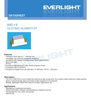
1. Product Overview
The 19-21/S2C-AL2M2VY/3T is a surface-mount device (SMD) LED utilizing AlGaInP chip technology to emit a brilliant orange color. This component is designed for modern, compact electronic assemblies, offering significant advantages in board space utilization and automated manufacturing processes.
1.1 Core Advantages and Product Positioning
Babban fa'idar wannan LED shine ƙaramin ƙafafunsa. Kasancewa ƙanƙanta sosai fiye da na gargajiya na nau'in LED na jagora, yana ba da damar ƙirar ƙananan allunan da'ira (PCBs), mafi girman yawan kayan aiki, rage buƙatun sararin ajiya, kuma a ƙarshe, ƙirƙirar kayan aiki na ƙarshe masu ƙanƙanta. Ginin sa mai nauyi ya ƙara sa ya zama zaɓi mai kyau don aikace-aikacen da girman da nauyi suke da matuƙar ƙarfi.
This LED is a mono-color type, is lead-free (Pb-free), and is compliant with major environmental and safety regulations including RoHS, EU REACH, and halogen-free standards (Br <900 ppm, Cl <900 ppm, Br+Cl < 1500 ppm). It is supplied in 8mm tape on 7-inch diameter reels, making it fully compatible with standard automatic pick-and-place equipment used in high-volume electronics manufacturing. The component is also compatible with both infrared and vapor phase reflow soldering processes.
2. Technical Specifications and In-Depth Interpretation
2.1 Absolute Maximum Ratings
These ratings define the limits beyond which permanent damage to the device may occur. Operation under these conditions is not guaranteed.
- Reverse Voltage (VR): 5V. Exceeding this voltage in reverse bias can cause junction breakdown.
- Forward Current (IF): 25mA (continuous).
- Peak Forward Current (IFP): 60mA (at a duty cycle of 1/10 and 1kHz frequency). This rating is for pulsed operation only.
- Power Dissipation (Pd): 60mW. This is the maximum power the package can dissipate without exceeding its thermal limits.
- Electrostatic Discharge (ESD) Human Body Model (HBM): 2000V. This indicates a moderate level of ESD sensitivity; proper ESD handling procedures are required.
- Operating Temperature (Topr): -40°C to +85°C. The device is rated for industrial temperature range applications.
- Storage Temperature (Tstg): -40°C to +90°C.
- Soldering Temperature: For reflow soldering, a peak temperature of 260°C for a maximum of 10 seconds is specified. For hand soldering, the iron tip temperature should not exceed 350°C for a maximum of 3 seconds per terminal.
2.2 Electro-Optical Characteristics
These parameters are measured at a standard test condition of an ambient temperature (Ta) of 25°C and a forward current (IF) of 5mA, unless otherwise noted.
- Luminous Intensity (Iv): Ranges from a minimum of 14.5 mcd to a maximum of 28.5 mcd. The typical value falls within this range. A tolerance of ±11% applies.
- Viewing Angle (2θ1/2): The half-intensity angle is typically 100 degrees, indicating a wide viewing pattern.
- Peak Wavelength (λp): Typically 611 nm.
- Dominant Wavelength (λd): Yana daga 600.5 nm zuwa 612.5 nm, tare da ƙimar kuskuren ±1 nm. Wannan ma'auni yana bayyana launin da ake gani.
- Faɗin Bakan (Δλ): Yawanci 17 nm, ana auna shi a rabin ƙarfin kololuwa (Faɗin Cikakke a Rabin Madaidaici).
- Ƙarfin Lantarki na Gaba (VF): Ranges from 1.70V to 2.20V at IF=5mA, with a tolerance of ±0.05V.
- Reverse Current (IR): Maximum of 10 μA when a reverse voltage (VR) of 5V is applied. Important Note: The device is not designed for operation in reverse bias; this test condition is for leakage current characterization only.
3. Binning System Explanation
To ensure color and brightness consistency in production, LEDs are sorted into bins based on key parameters.
3.1 Luminous Intensity Binning
Binned at IF = 5mA.
- L2: 14.5 mcd to 18.0 mcd
- M1: 18.0 mcd to 22.5 mcd
- M2: 22.5 mcd to 28.5 mcd
3.2 Dominant Wavelength Binning
Binned at IF = 5mA.
- D8: 600.5 nm to 603.5 nm
- D9: 603.5 nm to 606.5 nm
- D10: 606.5 nm to 609.5 nm
- D11: 609.5 nm to 612.5 nm
3.3 Forward Voltage Binning
Binned at IF = 5mA.
- 19: 1.70V to 1.80V
- 20: 1.80V to 1.90V
- 21: 1.90V to 2.00V
- 22: 2.00V to 2.10V
- 23: 2.10V to 2.20V
The product code "19-21" in the part number likely references specific bins from these categories (e.g., VF bin 19-21).
4. Performance Curve Analysis
Datasheet ina toa curves za kawaida muhimu kwa kubuni.
4.1 Spectral Distribution
Curve inaonyesha kilele kimoja kikuu karibu na 611 nm, ambacho ni sifa ya AlGaInP-based orange LEDs. Upana mwembamba (kawaida 17 nm) husababisha rangi ya machungwa iliyojaa na safi.
4.2 Relative Luminous Intensity vs. Forward Current
This curve is generally linear at lower currents but will show saturation effects as current increases. It is essential for determining the drive current needed to achieve a desired brightness level.
4.3 Relative Luminous Intensity vs. Ambient Temperature
The luminous intensity decreases as the ambient temperature increases. This curve is critical for applications operating over a wide temperature range, as it allows designers to derate the expected output or compensate in the drive circuitry.
4.4 Forward Current Derating Curve
This graph shows the maximum allowable continuous forward current as a function of ambient temperature. As temperature rises, the maximum current must be reduced to stay within the device's power dissipation limits and prevent thermal runaway.
4.5 Forward Voltage vs. Forward Current (I-V Curve)
This standard diode curve shows the exponential relationship. The forward voltage has a negative temperature coefficient, meaning it decreases slightly as the junction temperature increases.
4.6 Radiation Pattern
The polar diagram confirms the wide, lambertian-like emission pattern with a typical 100-degree viewing angle, providing even illumination over a broad area.
5. Mechanical and Package Information
5.1 Package Dimensions
The 19-21 SMD LED has a compact rectangular package. Key dimensions (in mm, tolerance ±0.1mm unless specified) include a body size of approximately 2.0mm in length and 1.25mm in width, with a height of about 0.8mm. The detailed drawing specifies pad locations, standoff height, and the position of the cathode identification mark.
5.2 Polarity Identification
A clear cathode mark is indicated on the package and the dimension drawing. Correct polarity must be observed during assembly to prevent reverse bias damage.
6. Soldering and Assembly Guidelines
6.1 Current Limiting
Mandatory: An external current-limiting resistor or constant-current driver must always be used in series with the LED. The LED's forward voltage has a sharp knee; a small increase in supply voltage can cause a large, potentially destructive increase in current.
6.2 Storage and Moisture Sensitivity
LEDs are packaged in a moisture-resistant barrier bag with desiccant.
- Do not open the bag until ready for use.
- After opening, unused LEDs should be stored at ≤30°C and ≤60% Relative Humidity.
- "Floor life" bayan buɗe jakar shine sa'o'i 168 (kwanaki 7).
- Idan an wuce lokacin fallasa ko mai nuna desiccant ya canza launi, dole ne a gasa kayan aikin a 60°C ±5°C na tsawon sa'o'i 24 kafin reflow soldering don hana lalacewar "popcorning".
6.3 Reflow Soldering Profile
A lead-free (Pb-free) reflow profile is specified:
- Pre-heating: 150-200°C for 60-120 seconds.
- Time Above Liquidus (TAL): Above 217°C for 60-150 seconds.
- Peak Temperature: Maximum of 260°C, held for a maximum of 10 seconds.
- Ramp-up Rate: Maximum 6°C/second.
- Ramp-down Rate: Maximum 3°C/second.
6.4 Hand Soldering and Rework
If hand soldering is necessary, use a soldering iron with a tip temperature <350°C, apply heat for ≤3 seconds per terminal, and use an iron with a power rating <25W. Allow a cooling interval of >2 seconds between terminals. Rework is strongly discouraged. If absolutely necessary, use a dual-tip soldering iron to simultaneously heat both terminals and lift the component to avoid pad damage. Always verify LED functionality after any rework.
7. Packaging and Ordering Information
7.1 Reel and Tape Specifications
LEDs are supplied in embossed carrier tape on 7-inch diameter reels. The tape width is 8mm. Each reel contains 3000 pieces. Detailed dimensions for the carrier tape pockets and the reel are provided in the datasheet.
7.2 Label Explanation
The reel label contains several key fields:
- CPN: Customer's Product Number
- P/N: Manufacturer's Product Number (e.g., 19-21/S2C-AL2M2VY/3T)
- QTY: Packing Quantity
- CAT: Luminous Intensity Rank (Bin Code, e.g., M1)
- HUE: Chromaticity Coordinates & Dominant Wavelength Rank (Bin Code, e.g., D10)
- REF: Forward Voltage Rank (Bin Code, e.g., 20)
- LOT No: Manufacturing Lot Number for traceability.
8. Application Suggestions
8.1 Typical Application Scenarios
- Automotive Interior: Backlighting for dashboard indicators, switches, and control panels.
- Telecommunications Equipment: Status indicators and keypad backlighting in phones, fax machines, and networking hardware.
- Consumer Electronics: Flat backlighting for small LCD displays, switch illumination, and symbolic indicators.
- General Purpose Indication: Power status, mode indication, and alert signals in a wide variety of electronic devices.
8.2 Design Considerations
- Drive Circuit: Always implement a constant-current source or a voltage source with a series resistor. Calculate the resistor value using R = (Vsupply - VF) / IF, where VF should be chosen from the maximum bin value (2.2V) for a robust design.
- Thermal Management: When power is low, ensure sufficient PCB copper area or thermal vias under the LED pads if operating at high ambient temperatures or near maximum current, to help dissipate heat and maintain light output stability.
- Optical Design: The wide 100-degree viewing angle makes it suitable for applications requiring broad-area illumination without secondary optics. For focused beams, a lens may be required.
- ESD Protection: Incorporate ESD protection diodes on sensitive signal lines if the LED is in a user-accessible location, as the device has a 2kV HBM rating.
9. Technical Comparison and Differentiation
Compared to older through-hole LED technologies, the 19-21 SMD LED offers:
- Size Reduction: Drastically smaller footprint and profile.
- Manufacturing Efficiency: Enables fully automated, high-speed assembly.
- Performance: AlGaInP technology provides high efficiency and good color saturation in the orange/red spectrum.
- Reliability: Solid SMD construction is generally more robust against vibration and mechanical shock than devices with wire bonds to a lead frame.
10. Frequently Asked Questions (FAQs)
Q: What is the difference between peak wavelength and dominant wavelength?
A: Peak wavelength (λp) is the wavelength at which the spectral power distribution is maximum. Dominant wavelength (λd) is the single wavelength of monochromatic light that matches the perceived color of the LED. For LEDs with a symmetric spectrum, they are often close, but λd is more relevant for color specification.
Q: Can I drive this LED at 20mA continuously?
A: Yes, the absolute maximum continuous forward current is 25mA, so 20mA is within specification. However, you must refer to the derating curve if the ambient temperature is significantly above 25°C, and ensure proper heat dissipation.
Q: Why is the reverse voltage rating only 5V?
A: This LED is not designed to be operated in reverse bias. The 5V rating is a test condition for measuring leakage current (IR). In circuit design, you must ensure the LED is never subjected to a reverse voltage, typically by ensuring it is correctly oriented or by placing a protection diode in parallel (anti-parallel) if the application necessitates it.
Q: How do I interpret the part number 19-21/S2C-AL2M2VY/3T?
A: Duk da cewa cikakken bayanin na iya zama na sirri, tsarin gama gari shi ne: "19-21" mai yiwuwa yana nuna kewayon kwandon ƙarfin gaba, "S2C" na iya nufin girman/ salon fakitin (2.0x1.25mm), "AL2M2VY" mai yiwuwa yana ɓoye kayan guntu (AlGaInP), launi (Brilliant Orange), da sauran siffofi, kuma "3T" na iya nuna fakitin tef da reel.
11. Practical Design Case Study
Labari: Designing a cluster of three orange status indicators for a consumer device powered by a 5V rail. The goal is uniform brightness and color.
Design Steps:
- Current Selection: Choose IF = 10mA for a good balance of brightness and longevity, well below the 25mA maximum.
- Voltage Calculation: Use the maximum VF from the datasheet (2.20V) for a conservative design. Series resistor R = (5V - 2.20V) / 0.010A = 280Ω. The nearest standard E24 value is 270Ω or 300Ω. Choosing 270Ω gives IF ≈ (5-2.2)/270 = 10.37mA.
- Power in Resistor: P = I2R = (0.01037)2 * 270 ≈ 0.029W. A standard 1/10W (0.1W) resistor is more than sufficient.
- Ensuring Uniformity: Dominant Wavelength bin (e.g., D10) da Luminous Intensity bin (e.g., M1) duk wani bin guda a lokacin oda, domin samun kamanni iri ɗaya. Yi amfani da resistor ɗaya ga kowane LED (maimakon resistor ɗaya ga duka a layi daya) don daidaita ƙananan VF bambance-bambance da kuma tabbatar da irin wannan halin yanzu.
- Tsari: Sanya LEDs tare da isasshen tazara don hana haɗin thermal. Bi shawarar tsarin fakitin daga zanen girma don ingantaccen soldering.
12. Technology Principle Introduction
The 19-21 LED is based on AlGaInP (Aluminum Gallium Indium Phosphide) semiconductor material. This compound semiconductor allows for the direct bandgap engineering necessary to produce efficient light emission in the orange, red, and yellow spectral regions. When a forward voltage is applied across the p-n junction, electrons and holes are injected into the active region where they recombine, releasing energy in the form of photons. The specific ratio of aluminum, gallium, and indium in the crystal lattice determines the bandgap energy and thus the wavelength (color) of the emitted light. The water-clear resin encapsulant protects the chip and acts as a primary lens, shaping the emitted light into the wide viewing angle pattern.
13. Industry Trends and Developments
The market for SMD LEDs like the 19-21 continues to evolve. Key trends include:
- Increased Efficiency: Ongoing material science and chip design improvements lead to higher luminous efficacy (more light output per electrical watt), allowing for lower drive currents and reduced system power consumption.
- Miniaturization: The drive for smaller devices pushes package sizes even smaller than the 19-21 (e.g., 1608, 1005 metric sizes), while maintaining or improving performance.
- Enhanced Reliability and Lifetime: Improvements in packaging materials, die attach, and wire bonding (or flip-chip designs) are extending operational lifetimes and improving performance under high-temperature and high-humidity conditions.
- Smart Integration: A broader trend involves integrating control circuitry, such as constant-current drivers or even addressable controllers (like WS2812), directly into the LED package, simplifying system design for complex lighting effects.
- Sustainability: The focus on halogen-free, lead-free, and REACH-compliant materials, as seen in this datasheet, is a standard industry requirement driven by global environmental regulations.
LED Specification Terminology
Complete explanation of LED technical terms
Photoelectric Performance
| Term | Unit/Representation | Simple Explanation | Why Important |
|---|---|---|---|
| Luminous Efficacy | lm/W (lumens per watt) | Light output per watt of electricity, higher means more energy efficient. | Directly determines energy efficiency grade and electricity cost. |
| Luminous Flux | lm (lumens) | Total light emitted by source, commonly called "brightness". | Determines if the light is bright enough. |
| Viewing Angle | ° (degrees), misal, 120° | Kwanar da ƙarfin haske ya ragu zuwa rabi, yana ƙayyade faɗin katako. | Yana shafar kewayon haskakawa da daidaito. |
| CCT (Color Temperature) | K (Kelvin), e.g., 2700K/6500K | Haske ko haske mai dumi/sanyi, ƙananan ƙimomi suna da rawaya/dumi, mafi girma fari/sanyi. | Yana ƙayyade yanayin haske da yanayin da ya dace. |
| CRI / Ra | Unitless, 0–100 | Ability to render object colors accurately, Ra≥80 is good. | Affects color authenticity, used in high-demand places like malls, museums. |
| SDCM | MacAdam ellipse steps, e.g., "5-step" | Color consistency metric, smaller steps mean more consistent color. | Ensures uniform color across same batch of LEDs. |
| Dominant Wavelength | nm (nanometers), e.g., 620nm (red) | Wavelength corresponding to color of colored LEDs. | Determines hue of red, yellow, green monochrome LEDs. |
| Spectral Distribution | Wavelength vs intensity curve | Shows intensity distribution across wavelengths. | Affects color rendering and quality. |
Electrical Parameters
| Term | Symbol | Simple Explanation | Design Considerations |
|---|---|---|---|
| Forward Voltage | Vf | Minimum voltage to turn on LED, like "starting threshold". | Driver voltage must be ≥Vf, voltages add up for series LEDs. |
| Forward Current | If | Current value for normal LED operation. | Usually constant current drive, current determines brightness & lifespan. |
| Max Pulse Current | Ifp | Peak current tolerable for short periods, used for dimming or flashing. | Pulse width & duty cycle must be strictly controlled to avoid damage. |
| Reverse Voltage | Vr | Max reverse voltage LED can withstand, beyond may cause breakdown. | Circuit must prevent reverse connection or voltage spikes. |
| Thermal Resistance | Rth (°C/W) | Resistance to heat transfer from chip to solder, lower is better. | High thermal resistance requires stronger heat dissipation. |
| ESD Immunity | V (HBM), e.g., 1000V | Ability to withstand electrostatic discharge, higher means less vulnerable. | Anti-static measures needed in production, especially for sensitive LEDs. |
Thermal Management & Reliability
| Term | Key Metric | Simple Explanation | Impact |
|---|---|---|---|
| Junction Temperature | Tj (°C) | Halin zazzabi na aiki a cikin LED chip. | Kowane raguwar 10°C na iya ninka tsawon rayuwa; yawan zafi yana haifar da raguwar haske, canjin launi. |
| Lumen Depreciation | L70 / L80 (hours) | Time for brightness to drop to 70% or 80% of initial. | Directly defines LED "service life". |
| Lumen Maintenance | % (e.g., 70%) | Percentage of brightness retained after time. | Indicates brightness retention over long-term use. |
| Color Shift | Δu′v′ or MacAdam ellipse | Degree of color change during use. | O nifa si iṣeṣi awọ ninu awọn iṣẹlẹ itansẹ. |
| Thermal Aging | Material degradation | Deterioration due to long-term high temperature. | May cause brightness drop, color change, or open-circuit failure. |
Packaging & Materials
| Term | Common Types | Simple Explanation | Features & Applications |
|---|---|---|---|
| Package Type | EMC, PPA, Ceramic | Housing material protecting chip, providing optical/thermal interface. | EMC: good heat resistance, low cost; Ceramic: better heat dissipation, longer life. |
| Chip Structure | Front, Flip Chip | Chip electrode arrangement. | Flip chip: better heat dissipation, higher efficacy, for high-power. |
| Phosphor Coating | YAG, Silicate, Nitride | Covers blue chip, converts some to yellow/red, mixes to white. | Different phosphors affect efficacy, CCT, and CRI. |
| Lens/Optics | Flat, Microlens, TIR | Optical structure on surface controlling light distribution. | Determines viewing angle and light distribution curve. |
Quality Control & Binning
| Term | Binning Content | Simple Explanation | Purpose |
|---|---|---|---|
| Luminous Flux Bin | Code e.g., 2G, 2H | Grouped by brightness, each group has min/max lumen values. | Ensures uniform brightness in same batch. |
| Voltage Bin | Code e.g., 6W, 6X | Grouped by forward voltage range. | Facilitates driver matching, improves system efficiency. |
| Kwandon Launi | 5-step MacAdam ellipse | Grouped by color coordinates, ensuring tight range. | Guarantees color consistency, avoids uneven color within fixture. |
| CCT Bin | 2700K, 3000K etc. | Grouped by CCT, each has corresponding coordinate range. | Meets different scene CCT requirements. |
Testing & Certification
| Term | Standard/Test | Simple Explanation | Significance |
|---|---|---|---|
| LM-80 | Lumen maintenance test | Long-term lighting at constant temperature, recording brightness decay. | Used to estimate LED life (with TM-21). |
| TM-21 | Life estimation standard | Estimates life under actual conditions based on LM-80 data. | Provides scientific life prediction. |
| IESNA | Illuminating Engineering Society | Covers optical, electrical, thermal test methods. | Industry-recognized test basis. |
| RoHS / REACH | Environmental certification | Ensures no harmful substances (lead, mercury). | Market access requirement internationally. |
| ENERGY STAR / DLC | Energy efficiency certification | Energy efficiency and performance certification for lighting. | Used in government procurement, subsidy programs, enhances competitiveness. |