Table of Contents
- 1. Product Overview
- 1.1 Core Features and Advantages
- 1.2 Target Applications
- 2. Technical Specifications and Objective Interpretation
- 2.1 Absolute Maximum Ratings
- 2.2 Photoelectric Characteristics
- 3. Binning System Description
- 3.1 Luminous Intensity Binning
- 3.2 Dominant Wavelength Binning
- 3.3 Forward Voltage Binning
- 4. Performance Curve Analysis
- 4.1 Relationship Between Relative Luminous Intensity and Ambient Temperature
- 4.2 Forward Current Derating Curve
- 4.3 Relationship between Forward Current and Forward Voltage (I-V Curve)
- 4.4 Relationship between Luminous Intensity and Forward Current
- 4.5 Spectral Distribution
- 4.6 Radiation Pattern Diagram
- 5. Mechanical and Packaging Information
- 5.1 Package Dimensions
- 5.2 Polarity Identification and Pad Design
- 6. Welding and Assembly Guide
- 6.1 Reflow Soldering Temperature Profile (Lead-Free)
- 6.2 Manual Soldering
- 6.3 Storage and Moisture Protection Requirements
- 7. Packaging and Ordering Information
- 7.1 Tape and Reel Specifications
- 7.2 Label Description
- 8. Application Design Considerations
- 8.1 Current Limiting Resistor Must Be Used
- 8.2 Thermal management.
- 8.3 ESD Protection
- 9. Technical Comparison and Differentiation
- 10. Frequently Asked Questions (FAQ)
- 10.1 What value of resistor should be used when using a 5V power supply?
- 10.2 Is it possible to omit the current-limiting resistor when using a constant current source for driving?
- 10.3 Why is the luminous intensity range so wide (18-45 mcd)?
- 10.4 How to interpret the part number 19-219/R6C-AM1N2VY/3T?
- 11. Design and Use Case Studies
- 12. Brief Introduction to Technical Principles
- 13. Industry Trends and Development
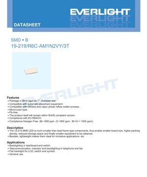
1. Product Overview
19-219 is a surface-mount device (SMD) LED designed for high-density, miniaturized applications. It utilizes AlGaInP chip technology to emit bright red light. Its primary advantage lies in its compact size, which significantly reduces PCB footprint, storage space, and overall device dimensions compared to traditional lead-frame LEDs. The device is lightweight and complies with modern manufacturing and environmental standards, including RoHS, REACH, and halogen-free requirements.
1.1 Core Features and Advantages
- Ultra-Compact Package:The small form factor (1.6mm x 0.8mm) enables higher packaging density and miniaturization of end products.
- Manufacturing Compatibility:Supplied in 8mm tape on 7-inch reels, fully compatible with automated surface-mount assembly equipment.
- Solder Joint Reliability:Compatible with infrared and vapor phase reflow soldering processes, suitable for high-volume production.
- Environmental Compliance:产品无铅,符合RoHS、REACH标准,并满足无卤素规格(Br <900ppm,Cl <900ppm,Br+Cl <1500ppm)。
- Monochrome Type:Emits a single bright red light.
1.2 Target Applications
This LED is ideal for applications requiring a small, reliable indicator or backlight in a confined space.
- Backlighting for dashboards and switches.
- Status indicators and keyboard backlighting in communication equipment (telephones, fax machines).
- Flat backlighting for LCD panels, switches, and symbols.
- General indicator light applications in consumer and industrial electronics.
2. Technical Specifications and Objective Interpretation
This section details the absolute maximum ratings and standard optoelectronic characteristics. Unless otherwise specified, all data are measured at an ambient temperature (Ta) of 25°C.
2.1 Absolute Maximum Ratings
These ratings define the limits beyond which permanent damage to the device may occur. Operation under these conditions is not guaranteed.
- Reverse Voltage (VR):5 V. Exceeding this voltage under reverse bias may cause junction breakdown.
- Continuous Forward Current (IF):25 mA. Direct current that can be continuously applied.
- Peak forward current (IFP):60 mA (duty cycle 1/10, 1kHz). Applicable only for pulse operation.
- Power consumption (Pd):60 mW. Maximum allowable power dissipation.
- Electrostatic discharge (ESD) human body model (HBM):2000 V. Indicates medium ESD sensitivity; standard ESD precautions are required.
- Operating temperature (Topr):-40°C to +85°C. The ambient temperature range for reliable operation.
- Storage temperature (Tstg):-40°C to +90°C.
- Soldering temperature:Reflow Soldering: Maximum 260°C for 10 seconds. Hand Soldering: Maximum 350°C per pin for 3 seconds.
2.2 Photoelectric Characteristics
In IFTypical performance parameters measured under = 5mA conditions.
- Luminous intensity (Iv):18 - 45 mcd (millicandela). A measure of perceived brightness. The broad range is managed through binning (see Section 3).
- Viewing angle (2θ1/2):130 degrees (typical). This wide viewing angle makes it suitable for applications where the LED may not be viewed head-on.
- Peak wavelength (λp):632 nm (typical). The wavelength at which the spectral output is strongest.
- Dominant wavelength (λd):617.5 - 633.5 nm. The single-wavelength perception of the emission color is also binned.
- Spectral bandwidth (Δλ):20 nm (typical). The width of the emission spectrum at half of its maximum intensity.
- Forward voltage (VF):1.7 - 2.2 V. Voltage drop across the LED when a 5mA current passes through. This parameter is binned to ensure design consistency.
- Reverse current (IR):at VR=5V is a maximum of 10 μA. A measure of leakage current in the off state.
Tolerance note:Luminous intensity tolerance is ±11%, dominant wavelength tolerance is ±1nm, forward voltage tolerance relative to the bin value is ±0.05V.
3. Binning System Description
To ensure color and brightness consistency in production, LEDs are sorted into different bins. The 19-219 employs three independent binning parameters.
3.1 Luminous Intensity Binning
Based on the luminous intensity measured at 5mA, LEDs are divided into four bins (M1, M2, N1, N2).
- M1:18.0 - 22.5 mcd
- M2:22.5 - 28.5 mcd
- N1:28.5 - 36.0 mcd
- N2:36.0 - 45.0 mcd
3.2 Dominant Wavelength Binning
LEDs are divided into four bins (E3, E4, E5, E6) to control precise red hue.
- E3:617.5 - 621.5 nm
- E4:621.5 - 625.5 nm
- E5:625.5 - 629.5 nm
- E6:629.5 - 633.5 nm
3.3 Forward Voltage Binning
LED e fa i vaega e lima (19, 20, 21, 22, 23) e fa'avasega ai masini e tutusa uiga fa'aeletise, e fesoasoani i le fa'afetauiina o le taimi i mamanu LED e tele.
- 19:1.7 - 1.8 V
- 20:1.8 - 1.9 V
- 21:1.9 - 2.0 V
- 22:2.0 - 2.1 V
- 23:2.1 - 2.2 V
4. Performance Curve Analysis
The datasheet provides several key graphs illustrating the behavior of the LED under different conditions.
4.1 Relationship Between Relative Luminous Intensity and Ambient Temperature
This curve shows that the luminous intensity decreases as the ambient temperature increases. The output is relatively stable from -40°C to approximately 25°C, but the decline becomes more pronounced at higher temperatures, which is typical behavior for LEDs due to increased non-radiative recombination.
4.2 Forward Current Derating Curve
This graph defines the maximum allowable forward current as a function of ambient temperature. To prevent overheating and ensure long-term reliability, the forward current must be reduced when operating in high-temperature environments (approximately above 25°C).
4.3 Relationship between Forward Current and Forward Voltage (I-V Curve)
This fundamental characteristic demonstrates an exponential relationship between current and voltage. This curve is crucial for designing current-limiting circuits, typically series resistors. The "knee point" where the curve begins to conduct is approximately between 1.6V and 1.7V.
4.4 Relationship between Luminous Intensity and Forward Current
This graph shows that the light output increases with the forward current, but the relationship is not entirely linear, especially at higher currents. It helps designers select an operating point that balances brightness, efficiency, and device stress.
4.5 Spectral Distribution
The spectral output graph shows a single peak centered at approximately 632 nm (typical), confirming a monochromatic bright red emission with a typical full width at half maximum (FWHM) of 20 nm.
4.6 Radiation Pattern Diagram
The polar plot illustrates a viewing angle of 130 degrees, showing the angular distribution of light intensity, which is close to a Lambertian (cosine) distribution.
5. Mechanical and Packaging Information
5.1 Package Dimensions
LED has a very compact footprint, key dimensions are as follows (unit: mm, tolerance ±0.1mm, unless otherwise specified):
- Tsayi: 1.60
- Faɗi: 0.80
- Height: 0.65 ±0.1
- Cathode pad size: 0.70 x 0.20 ±0.05
5.2 Polarity Identification and Pad Design
The cathode (negative terminal) is clearly marked on the top of the package. A recommended pad layout is provided to ensure reliable solder joints and correct alignment during the reflow process. The datasheet notes that the pad dimensions are for reference only and can be modified according to specific PCB design requirements.
6. Welding and Assembly Guide
Proper handling is crucial for the reliability of SMD components.
6.1 Reflow Soldering Temperature Profile (Lead-Free)
Recommended specific temperature profile:
- Preheat:150-200°C for 60-120 seconds.
- Time above liquidus (TAL):Maintain at above 217°C for 60-150 seconds.
- Peak Temperature:Maximum 260°C, hold time up to 10 seconds.
- Heating/Cooling Rate:Maximum heating rate 6°C/s, maximum cooling rate 3°C/s.
Important Note:The reflow soldering of the same LED should not exceed two times.
6.2 Manual Soldering
If manual soldering is required, extra caution must be taken:
- Use a soldering iron with a tip temperature below 350°C.
- Limit the soldering time for each pin to within 3 seconds.
- Use a soldering iron with a power of 25W or lower.
- Allow at least 2 seconds between soldering each pin to prevent thermal shock.
6.3 Storage and Moisture Protection Requirements
LED e wa a ni ɗaki mai bushewa a cikin jakar da ba ta da ɗanɗano.
- Kafin buɗewa:Ajiye a ≤30°C da ≤90% zafi na yanayi (RH).
- After Opening (Floor Life):1 year under conditions of ≤30°C and ≤60% RH. Unused LEDs should be resealed in moisture barrier packaging.
- Baking:If the desiccant indicator changes color or the storage time is exceeded, the LED should be baked at 60 ±5°C for 24 hours before using the reflow soldering process.
7. Packaging and Ordering Information
7.1 Tape and Reel Specifications
Components are supplied in 8mm wide embossed carrier tape, wound on standard 7-inch (178mm) diameter reels. Each reel contains 3000 pieces.
7.2 Label Description
The reel label contains several key codes to identify the specific binning characteristics of the LEDs on that reel:
- CAT:Luminous Intensity Grade (e.g., M1, N2).
- HUE:Chromaticity/Dominant Wavelength Grade (e.g., E4, E5).
- REF:Forward Voltage Grade (e.g., 20, 21).
- Other information includes Customer Part Number (CPN), Manufacturer Part Number (P/N), Quantity (QTY), and Lot Number (LOT No).
8. Application Design Considerations
8.1 Current Limiting Resistor Must Be Used
The datasheet clearly warns that an external current-limiting resistor is mandatory. LEDs exhibit a steep exponential I-V characteristic; a small increase in voltage can lead to a large, even destructive, increase in current. The resistor value (R) can be calculated using Ohm's Law: R = (VPower supply- V) / I, where VFis the forward voltage from binning or typical characteristics, IFis the desired operating current (≤25mA DC).F8.2 Thermal management.FAlthough it is a low-power device, thermal considerations remain important for its lifespan. At elevated ambient temperatures, the forward current derating curve must be followed. Ensure the PCB pad design provides sufficient thermal dissipation when necessary, even though the recommended pads are primarily for electrical and mechanical connections.
8.3 ESD Protection
The ESD rating is 2000V (HBM). Standard ESD prevention measures should be followed during operation and assembly to prevent potential damage.
9. Technical Comparison and Differentiation
The primary differentiation of the 19-219 LED lies in its combination of an extremely small 1.6mm x 0.8mm footprint with a relatively wide 130-degree viewing angle and a comprehensive three-parameter binning system (intensity, wavelength, voltage). This enables designers to achieve consistent optical performance in space-constrained applications where visual uniformity is critical, such as multi-LED backlight arrays or indicator panels. It offers higher density compared to larger SMD LEDs or through-hole LEDs. Compared to other miniature LEDs, its detailed binning provides stronger control over the final product's appearance.
10. Frequently Asked Questions (FAQ)
10.1 What value of resistor should be used when using a 5V power supply?
Using maximum typical V
Value 2.2V and target I
Value 20mA (with margin): R = (5V - 2.2V) / 0.020A = 140 ohms. The nearest standard value of 150 ohms will result in IF≈ 18.7mA, which is safe and provides good brightness. Always base calculations on the actual VFValidate the value.F10.2 Is it possible to omit the current-limiting resistor when using a constant current source for driving?FYes, a constant current driver set to the desired current (e.g., 20mA) is an excellent alternative to a series resistor, providing more stable performance across temperature and voltage variations.
10.3 Why is the luminous intensity range so wide (18-45 mcd)?
This is a natural variation in the manufacturing process. The binning system (M1, M2, N1, N2) classifies LEDs into tighter groups. To ensure consistent brightness in the application, specify and use LEDs from the same luminous intensity bin.
10.4 How to interpret the part number 19-219/R6C-AM1N2VY/3T?
This part number is a manufacturer-specific code. The key selection information is contained in the independent binning codes (CAT, HUE, REF) on the reel label, which define the device's actual luminous intensity, dominant wavelength, and forward voltage.
11. Design and Use Case Studies
Scenario: Design a compact status indicator panel containing 20 uniformly bright red LEDs.
Specification Selection:
Select the N1 luminous intensity bin (28.5-36.0 mcd) to achieve sufficient brightness. Select the E4 wavelength bin (621.5-625.5 nm) to achieve a consistent red hue. If using independent series resistors, the forward voltage bin has a lesser impact on uniformity, but selecting the same bin (e.g., 20) can simplify resistor value calculations.
- Schematic:Each LED is connected in parallel from a common voltage rail (e.g., 3.3V), with each LED having its own current-limiting resistor. The resistor value is calculated based on the nominal V
- value of the selected voltage bin.PCB Layout:FUse recommended or modified pad layout. Ensure the cathode marking on PCB silkscreen matches LED polarity. Arrange LEDs closely to achieve panel effect.
- Assembly:Strictly follow the reflow soldering temperature profile. Do not exceed two reflow cycles. Properly store opened reels if not used immediately.
- Result:Thanks to the small size and precise binning of the 19-219 LED, a high-density indicator panel with consistent color and brightness is achieved.
- 12. Brief Introduction to Technical PrinciplesThe 19-219 LED is based on AlGaInP (aluminum gallium indium phosphide) semiconductor material. When a forward voltage is applied across the p-n junction, electrons and holes are injected into the active region where they recombine. In AlGaInP LEDs, this recombination releases energy in the form of photons (light) within the red to amber portion of the visible spectrum. The specific composition of the AlGaInP layer determines the peak wavelength, which in this case is tuned for bright red emission at approximately 632 nm. The epoxy encapsulant is water-white to maximize light extraction efficiency and also serves to protect the semiconductor chip.
13. Industry Trends and Development
The market for miniature SMD LEDs like the 19-219 continues to be driven by the trend towards increasing miniaturization and slimming of electronic devices. Key developments in the broader LED industry affecting such components include:
Efficiency Improvements:
Continuous improvements in materials and processes lead to higher luminous efficacy (more light output per watt of electrical power), thereby allowing the use of lower operating currents and reduced power consumption in end products.
- Enhanced Color Consistency:Advanced binning and wafer-level testing enable stricter control over chromaticity and intensity, which is crucial for applications like display backlighting where uniformity is paramount.
- Reliability and Lifetime Improvement:Improvements in packaging materials and chip design continue to extend operational lifetime and enhance robustness against thermal and environmental stress.
- Integration:Although discrete LEDs remain essential, there is a parallel trend towards integrated LED modules and light guides for more complex lighting solutions, though discrete components offer maximum design flexibility for custom layouts.
- 19-219 represents a mature, well-characterized component that benefits from ongoing industry advancements in materials science and manufacturing precision.While discrete LEDs remain essential, there is a parallel trend towards integrated LED modules and light guides for more complex lighting solutions, though discrete components offer maximum design flexibility for custom layouts.
The 19-219 represents a mature, well-characterized component that benefits from these ongoing industry advancements in materials science and manufacturing precision.
Detailed Explanation of LED Specification Terminology
Complete Explanation of LED Technical Terminology
I. Core Indicators of Photoelectric Performance
| Terminology | Unit/Representation | Popular Explanation | Why It Is Important |
|---|---|---|---|
| Luminous Efficacy | lm/W (lumens per watt) | The luminous flux emitted per watt of electrical energy, the higher the more energy-efficient. | Directly determines the energy efficiency class and electricity cost of the luminaire. |
| Luminous Flux | lm (lumen) | The total amount of light emitted by a light source, commonly known as "brightness". | Determine if the lamp is bright enough. |
| Viewing Angle | ° (degrees), such as 120° | The angle at which light intensity drops to half, determining the beam's width. | Affects the illumination range and uniformity. |
| Color Temperature (CCT) | K (Kelvin), e.g., 2700K/6500K | The warmth or coolness of light color; lower values are yellowish/warm, higher values are whitish/cool. | Determines the lighting atmosphere and suitable application scenarios. |
| Color Rendering Index (CRI / Ra) | No unit, 0–100 | The ability of a light source to reproduce the true colors of objects, Ra≥80 is recommended. | Affects color fidelity, used in high-demand places such as shopping malls and art galleries. |
| Color Tolerance (SDCM) | MacAdam Ellipse Steps, e.g., "5-step" | Quantitative indicator of color consistency, the smaller the step number, the more consistent the color. | Ensure no color difference among the same batch of luminaires. |
| Dominant Wavelength | nm (nanometer), e.g., 620nm (red) | The wavelength value corresponding to the color of a colored LED. | Determine the hue of monochromatic LEDs such as red, yellow, and green. |
| Spectral Distribution | Wavelength vs. Intensity Curve | Shows the intensity distribution of light emitted by an LED across various wavelengths. | Affects color rendering and color quality. |
II. Electrical Parameters
| Terminology | Symbols | Popular Explanation | Design Considerations |
|---|---|---|---|
| Forward Voltage | Vf | Minimum voltage required to turn on an LED, similar to a "starting threshold". | The driving power supply voltage must be ≥ Vf, and the voltage adds up when multiple LEDs are connected in series. |
| Forward Current | If | The current value that allows the LED to emit light normally. | A cikin yawancin lokuta ana amfani da tuƙi mai tsayayyen ƙarfi, ƙarfin lantarki yana ƙayyadaddun haske da rayuwa. |
| Mafi girman ƙarfin bugun jini (Pulse Current) | Ifp | Peak current that can be withstood in a short time, used for dimming or flashing. | Pulse width and duty cycle must be strictly controlled, otherwise overheating damage will occur. |
| Reverse Voltage | Vr | The maximum reverse voltage that an LED can withstand; exceeding it may cause breakdown. | A cikin da'ira, ya kamata a hana haɗin baya ko kuma ƙarfin lantarki mai ƙarfi. |
| Thermal Resistance | Rth (°C/W) | The resistance to heat flow from the chip to the solder joint. A lower value indicates better heat dissipation. | High thermal resistance requires a more robust heat dissipation design; otherwise, the junction temperature will increase. |
| Electrostatic Discharge Immunity (ESD Immunity) | V (HBM), such as 1000V | Anti-static strike capability, the higher the value, the less susceptible to damage from static electricity. | Anti-static measures must be implemented during production, especially for high-sensitivity LEDs. |
III. Thermal Management and Reliability
| Terminology | Key Indicators | Popular Explanation | Impact |
|---|---|---|---|
| Junction Temperature | Tj (°C) | The actual operating temperature inside the LED chip. | For every 10°C reduction, the lifespan may double; excessively high temperatures lead to lumen depreciation and color shift. |
| Lumen Depreciation | L70 / L80 (hours) | The time required for brightness to drop to 70% or 80% of its initial value. | Directly defines the "useful life" of an LED. |
| Lumen Maintenance | % (e.g., 70%) | The percentage of remaining brightness after a period of use. | Characterizes the ability to maintain brightness after long-term use. |
| Color Shift | Δu′v′ or MacAdam Ellipse | The degree of color change during use. | Affects the color consistency of the lighting scene. |
| Thermal Aging | Material performance degradation | Degradation of packaging materials due to long-term high temperature. | May lead to decreased brightness, color shift, or open-circuit failure. |
IV. Encapsulation and Materials
| Terminology | Common Types | Popular Explanation | Characteristics and Applications |
|---|---|---|---|
| Package Type | EMC, PPA, Ceramic | The housing material that protects the chip and provides optical and thermal interfaces. | EMC has good heat resistance and low cost; ceramic has excellent heat dissipation and long lifespan. |
| Chip structure | Front Side, Flip Chip | Chip Electrode Layout Method. | Flip-chip offers better heat dissipation and higher luminous efficacy, suitable for high-power applications. |
| Phosphor coating | YAG, Silicate, Nitride | Covered on the blue light chip, partially converted into yellow/red light, mixed into white light. | Different phosphors affect luminous efficacy, color temperature, and color rendering. |
| Lens/Optical Design | Flat, Microlens, Total Internal Reflection | Optical structure on the encapsulation surface, controlling light distribution. | Determines the emission angle and light distribution curve. |
V. Quality Control and Binning
| Terminology | Bin Content | Popular Explanation | Purpose |
|---|---|---|---|
| Luminous Flux Binning | Codes such as 2G, 2H | Grouped by brightness level, each group has a minimum/maximum lumen value. | Ensure uniform brightness for products within the same batch. |
| Voltage binning | Codes such as 6W, 6X | Grouped by forward voltage range. | Facilitates driver power matching and improves system efficiency. |
| Color Grading | 5-step MacAdam Ellipse | Group by color coordinates to ensure colors fall within a minimal range. | Ensure color consistency to avoid uneven colors within the same luminaire. |
| Color temperature binning | 2700K, 3000K, etc. | Grouped by color temperature, each group has a corresponding coordinate range. | To meet the color temperature requirements of different scenarios. |
Six, Testing and Certification
| Terminology | Standard/Test | Popular Explanation | Meaning |
|---|---|---|---|
| LM-80 | Lumen Maintenance Test | Long-term illumination under constant temperature conditions, recording brightness attenuation data. | Used to estimate LED lifetime (combined with TM-21). |
| TM-21 | Standard for Life Projection | Projecting the lifespan under actual use conditions based on LM-80 data. | Provide scientific life prediction. |
| IESNA standard | Standard of the Illuminating Engineering Society | Covers optical, electrical, and thermal testing methods. | Industry-recognized testing basis. |
| RoHS / REACH | Environmental certification | Ensure the product does not contain harmful substances (e.g., lead, mercury). | Entry requirements for the international market. |
| ENERGY STAR / DLC | Energy Efficiency Certification | Energy efficiency and performance certification for lighting products. | Yawan da ake amfani da shi a cikin sayayyar gwamnati da ayyukan tallafi, don haɓaka gasar kasuwa. |