Table of Contents
- 1. Product Overview
- 1.1 Product Positioning and Core Advantages
- 1.2 Target Market and Applications
- 2. Technical Parameter Deep Dive
- 2.1 Absolute Maximum Ratings
- 2.2 Electro-Optical Characteristics
- 3. Binning System Explanation
- 3.1 Luminous Intensity Binning
- 3.2 Dominant Wavelength Binning
- 4. Mechanical and Package Information
- 4.1 Package Dimensions
- 4.2 Polarity Identification
- 5. Soldering and Assembly Guide
- 5.1 Reflow Soldering Profile
- 5.2 Storage and Moisture Sensitivity
- 5.3 Hand Soldering and Rework
- 6. Packaging and Ordering Information
- 6.1 Standard Packaging
- 6.2 Label Explanation
- 7. Application Suggestions and Design Considerations
- 7.1 Current Limiting is Mandatory
- 7.2 Thermal Management
- 7.3 ESD Precautions
- 8. Technical Comparison and Differentiation
- 9. Frequently Asked Questions (Based on Technical Parameters)
- 9.1 Ina iya fitar da wannan LED ba tare da resistor mai iyakancewar halin yanzu ba?
- 9.2 Me ya sa ƙimar ƙarfin lantarki ta baya kawai 5V, kuma ma'anar bayanin ta nufi me?
- 9.3 Ta yaya zan zaɓi lambar kwandon da ta dace?
- 10. Nazarin Ƙira da Amfani
- 10.1 Designing a Compact Status Indicator Panel
- 11. Operating Principle Introduction
- 12. Technology Trends and Context
1. Product Overview
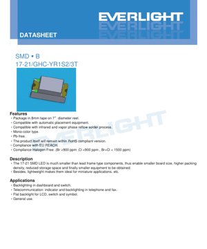
The 17-21/GHC-YR1S2/3T is a surface-mount device (SMD) LED designed for modern, compact electronic applications. This component represents a significant advancement over traditional lead-frame LEDs, offering substantial benefits in terms of board space utilization and assembly efficiency.
1.1 Product Positioning and Core Advantages
Wannan LED na mono-color ne, yana fitar da haske mai haske kore. Babban fa'idarsa ta ta'allaka ne a cikin ƙaramin ƙafafunsa. Girman da ya fi ƙanƙanta idan aka kwatanta da abubuwan da ke da gubar yana bawa masu ƙira damar samun mafi girman yawan tattarawa akan allunan da'ira da aka buga (PCBs). Wannan kai tsaye yana fassara zuwa rage girman allo, rage buƙatun ajiya na abubuwan haɗin gwiwa, kuma a ƙarshe, ƙirƙirar ƙananan kayan aiki masu amfani da ƙarshe da sauƙi. Yanayin nauyin fakitin ya ƙara sa ya zama zaɓi mai kyau don aikace-aikacen da nauyi ke da mahimmanci.
1.2 Target Market and Applications
Na'urar tana nufin kewayon masu amfani da masana'antu. Aikace-aikacenta na yau da kullun sun haɗa da hasken baya na allunan kayan aiki, maɓallai, da alamomi. Hakanan ya dace da amfani a cikin kayan aikin sadarwa azaman alamomin yanayi ko hasken baya na na'urori kamar wayoyi da na'urorin faks. Bugu da ƙari, yana aiki azaman fitilar nuni ta gama gari a cikin samfuran lantarki daban-daban.
2. Technical Parameter Deep Dive
This section provides a detailed, objective analysis of the LED's key technical parameters as defined in the datasheet.
2.1 Absolute Maximum Ratings
The absolute maximum ratings define the limits beyond which permanent damage to the device may occur. These are not operating conditions.
- Reverse Voltage (VR): 5V. It is crucial to note that this rating is specified for infrared (IR) test conditions only. The datasheet explicitly states the device is not designed for reverse operation in an actual circuit. Exceeding this voltage in reverse bias can cause immediate failure.
- Forward Current (IF): 25 mA. This is the maximum continuous DC current that can be applied to the LED.
- Peak Forward Current (IFP): 100 mA. This is the maximum pulsed current, permissible only under a duty cycle of 1/10 at 1 kHz. This parameter is relevant for multiplexing or PWM dimming applications but must be used with caution to avoid overheating.
- Power Dissipation (Pd): 95 mW. This is the maximum power the package can dissipate, calculated from the forward voltage and current limits, and is critical for thermal management.
- Operating & Storage Temperature: The device can operate from -40°C to +85°C and be stored from -40°C to +90°C. This wide range makes it suitable for harsh environments.
- Soldering Temperature: For reflow soldering, a peak temperature of 260°C for a maximum of 10 seconds is specified. For hand soldering, the iron tip temperature must not exceed 350°C, and contact time should be limited to 3 seconds per terminal.
2.2 Electro-Optical Characteristics
These parameters are measured at a standard test condition of a forward current (IF) of 20 mA and an ambient temperature (Ta) of 25°C.
- Luminous Intensity (Iv): Ranges from a minimum of 112.0 mcd to a maximum of 285.0 mcd. The typical value is not specified, indicating performance is managed through a binning system (detailed later). The tolerance is ±11%.
- Viewing Angle (2θ1/2): A typical value of 140 degrees. This wide viewing angle makes the LED suitable for applications requiring broad illumination or visibility from multiple angles.
- Peak Wavelength (λp): Typically 518 nm, placing it in the brilliant green region of the visible spectrum.
- Dominant Wavelength (λd): Ranges from 520.0 nm to 535.0 nm, with a tight tolerance of ±1 nm. This parameter is more closely related to the perceived color of the light.
- Spectral Bandwidth (Δλ): Yawanci 35 nm, yana bayyana yaduwar tsayin raƙuman hasken da ake fitarwa a kusa da kololuwar.
- Forward Voltage (VF): Typically 3.5V, with a maximum of 4.0V at 20 mA. This is a critical parameter for circuit design, as it determines the voltage drop across the LED and the necessary current-limiting resistor value.
- Reverse Current (IR): Maximum of 50 μA at a reverse voltage of 5V (test condition).
3. Binning System Explanation
To ensure consistent performance, the LEDs are sorted into bins based on key optical parameters. This allows designers to select parts that meet specific brightness and color requirements.
3.1 Luminous Intensity Binning
LEDs are categorized into four bins (R1, R2, S1, S2) based on their measured luminous intensity at 20 mA.
- Bin R1: 112.0 – 140.0 mcd
- Bin R2: 140.0 – 180.0 mcd
- Bin S1: 180.0 – 225.0 mcd
- Bin S2: 225.0 – 285.0 mcd
The selection of a higher bin (e.g., S2) guarantees higher minimum brightness, which is essential for applications requiring high visibility or where multiple LEDs need to be matched for uniform appearance.
3.2 Dominant Wavelength Binning
LEDs are also binned by their dominant wavelength into three groups (X, Y, Z) to control color consistency.
- Bin X: 520.0 – 525.0 nm
- Bin Y: 525.0 – 530.0 nm
- Bin Z: 530.0 – 535.0 nm
For applications where color matching between multiple LEDs is critical (e.g., status bars, backlight arrays), specifying a single, narrow bin is necessary to avoid visible color differences.
4. Mechanical and Package Information
4.1 Package Dimensions
The 17-21 SMD LED has a compact rectangular package. Key dimensions include a length of 1.6 mm, a width of 0.8 mm, and a height of 0.6 mm (tolerance ±0.1 mm unless otherwise noted). The datasheet provides a detailed dimensional drawing including pad layout, which is essential for creating the PCB footprint. Correct pad design ensures proper soldering, alignment, and thermal performance.
4.2 Polarity Identification
The cathode is typically identified by a marking on the package or a specific pad geometry (e.g., a chamfered corner). Correct polarity orientation during placement is vital for the circuit to function.
5. Soldering and Assembly Guide
Proper handling and soldering critical to reliability and performance of SMD LEDs.
5.1 Reflow Soldering Profile
The datasheet specifies a lead-free reflow soldering profile. Key phases include:
- Pre-heating: Ramp from ambient to 150-200°C over 60-120 seconds.
- Soak/Reflow: Time above liquidus (217°C) should be 60-150 seconds. The peak temperature must not exceed 260°C, and the time at or above 255°C must be limited to a maximum of 30 seconds.
- Cooling: The maximum cooling rate should not exceed 6°C per second.
Critical Note: Reflow soldering should not be performed more than two times on the same LED assembly to prevent thermal damage to the package and die.
5.2 Storage and Moisture Sensitivity
This component is moisture-sensitive. Precautions include:
- Do not open the moisture-proof barrier bag until the components are ready for use.
- After opening, unused LEDs must be stored at ≤30°C and ≤60% relative humidity.
- The "floor life" after bag opening is 168 hours (7 days). If not used within this time, the LEDs must be rebaked at 60 ±5°C for 24 hours before use.
- Idan mai nuna desiccant ya canza launi, ana buƙatar gasa ba tare da la'akari da lokaci ba.
5.3 Hand Soldering and Rework
Idan ba za a iya guje wa sayar da hannu ba, dole ne a yi taka tsantsan sosai:
- Zazzabi na ƙarshen ƙarfe na sayarwa dole ne ya zama ≤350°C.
- Lokacin tuntuɓar kowane tasha dole ne ya zama ≤3 seconds, tare da tazarar aƙalla seconds 2 tsakanin sayar da kowane tasha don ba da damar sanyaya.
- Repair after soldering is strongly discouraged. If absolutely necessary, a dual-head soldering iron should be used to simultaneously heat both terminals, minimizing thermal stress. The impact on LED characteristics must be verified beforehand.
6. Packaging and Ordering Information
6.1 Standard Packaging
LEDs are supplied in moisture-resistant packaging, which includes:
- Components placed in an 8mm wide carrier tape.
- The tape is wound on a 7-inch diameter reel.
- A standard reel contains 3000 pieces.
- The reel is placed inside an aluminum moisture-proof bag with a desiccant packet and a humidity indicator card.
6.2 Label Explanation
The reel label contains codes that specify the exact characteristics of the LEDs on that reel:
- P/N: Product Number (e.g., 17-21/GHC-YR1S2/3T).
- CAT: Luminous Intensity Rank (corresponds to the bin code: R1, R2, S1, S2).
- HUE: Chromaticity Coordinates & Dominant Wavelength Rank (corresponds to the bin code: X, Y, Z).
- REF: Forward Voltage Rank.
- LOT No: Traceable manufacturing lot number.
7. Application Suggestions and Design Considerations
7.1 Current Limiting is Mandatory
An external current-limiting resistor is absolutely required. LEDs are current-driven devices. A small increase in forward voltage can cause a large, potentially destructive increase in forward current. The resistor value (R) can be calculated using Ohm's Law: R = (V_supply - VF_LED) / I_desired. Always design for the *typical* VF to ensure current is within limits if the actual VF is at the minimum specified value.
7.2 Thermal Management
While small, the LED generates heat. The 95 mW power dissipation limit must be respected. Ensure the PCB pad design provides adequate thermal relief, especially if operating at or near the maximum continuous current (25 mA). Avoid placing the LED near other heat-generating components.
7.3 ESD Precautions
The device has an ESD rating of 1000V (Human Body Model). Standard ESD handling procedures should be followed during assembly and handling to prevent latent damage that may not cause immediate failure but can degrade long-term reliability.
8. Technical Comparison and Differentiation
The primary differentiation of the 17-21 LED lies in its form factor and performance balance.
- vs. Larger SMD LEDs (e.g., 3528, 5050): It offers a significantly smaller footprint, enabling higher-density designs, but typically at a lower total light output per device.
- vs. Chip-Scale Packages (CSP): It is larger than cutting-edge CSP LEDs but is easier to handle with standard SMT equipment and offers a more robust package for many applications.
- vs. Leaded LEDs: It eliminates the need for through-holes, enables automated pick-and-place assembly, reduces parasitic inductance, and allows for much smaller and lighter end products.
9. Frequently Asked Questions (Based on Technical Parameters)
9.1 Ina iya fitar da wannan LED ba tare da resistor mai iyakancewar halin yanzu ba?
No. This is explicitly warned against in the "Precautions For Use" section. The forward voltage has a range (typ. 3.5V, max. 4.0V). Connecting it directly to a voltage source even slightly above its VF will cause excessive current, leading to rapid overheating and failure. A series resistor is mandatory for safe operation.
9.2 Me ya sa ƙimar ƙarfin lantarki ta baya kawai 5V, kuma ma'anar bayanin ta nufi me?
5V rating no yɛ IR (reverse leakage current) a wɔde hwehwɛ mu nko ara. Datasheet no kyerɛkyerɛ mu pefee se, "Wɔammɔɛ sɛnea wɔde adwuma reverse mu." Circuit mu no, wɔhia sɛ wuhwɛ koraa na LED no mfa reverse bias biara nhyia, efirisɛ ɛnyɛ Zener diode, na voltage a ɛboro 5V no, reverse-biased a, ɛbɛyɛ a ɛsɛe. Circuit a reverse voltage betumi aba mu no (te sɛ AC coupling, inductive loads), fa protection diodes di dwuma.
9.3 Ta yaya zan zaɓi lambar kwandon da ta dace?
Zaɓi kwandon bisa ga bukatun aikace-aikacenku:
10. Nazarin Ƙira da Amfani
10.1 Designing a Compact Status Indicator Panel
Scenario: Designing a dense panel of 20 status indicators for a networking device. Uniform brightness and color are important for user experience. Design Steps: 1. Current Setting: Choose a drive current of 15 mA (below the 25 mA max) for good brightness and longevity. Calculate resistor value for a 5V supply: R = (5V - 3.5V) / 0.015A = 100 Ohms. Use a 1% tolerance resistor. Binning Selection: To ensure uniformity, specify all LEDs from the same luminous intensity bin (e.g., S1) and the same dominant wavelength bin (e.g., Y). This information must be provided when ordering. PCB Layout: Use the exact pad dimensions from the datasheet. Provide a small thermal relief connection for each pad to aid soldering and prevent tombstoning, but ensure the copper area is sufficient for heat dissipation. Assembly: Follow the specified reflow profile. Keep the panels in sealed bags until the moment they are loaded into the pick-and-place machine to respect the 7-day floor life.
11. Operating Principle Introduction
The 17-21/GHC-YR1S2/3T LED is based on a semiconductor chip made of Indium Gallium Nitride (InGaN), as indicated in the Device Selection Guide. When a forward voltage exceeding the diode's built-in potential is applied, electrons and holes are injected into the active region of the semiconductor. Their recombination releases energy in the form of photons (light). The specific composition of the InGaN material determines the bandgap energy, which directly correlates to the wavelength (color) of the emitted light—in this case, brilliant green (~518 nm peak). The water-clear resin encapsulant protects the chip and acts as a lens, shaping the 140-degree viewing angle of the emitted light.
12. Technology Trends and Context
The 17-21 package represents a mature and widely adopted form factor in the SMD LED market. The general trend in LED technology continues towards several key areas relevant to such components:
- Increased Efficiency: Ongoing material science improvements aim to produce more lumens per watt (higher efficacy), meaning brighter light or lower power consumption for the same size package.
- Miniaturization: While the 17-21 (1.6x0.8mm) is small, the industry pushes towards even smaller chip-scale packages (CSP) that are nearly the size of the bare semiconductor die, enabling ultra-high-density lighting arrays.
- Improved Color Consistency: Advances in epitaxial growth and binning processes allow for tighter control over dominant wavelength and luminous intensity, reducing the need for stringent bin selection in some applications.
- Enhanced Reliability: Improvements in packaging materials, such as more robust silicones and phosphors (for white LEDs), and better thermal management designs extend operational lifetime and allow for use in higher-temperature environments.
This datasheet reflects a reliable, well-characterized component that balances performance, size, and manufacturability for a broad range of mainstream electronic applications.
LED Specification Terminology
Complete explanation of LED technical terms
Photoelectric Performance
| Term | Unit/Representation | Simple Explanation | Why Important |
|---|---|---|---|
| Luminous Efficacy | lm/W (lumens per watt) | Light output per watt of electricity, higher means more energy efficient. | Directly determines energy efficiency grade and electricity cost. |
| Luminous Flux | lm (lumens) | Total light emitted by source, commonly called "brightness". | Determines if the light is bright enough. |
| Viewing Angle | ° (degrees), e.g., 120° | Kwanin da ƙarfin haske ya ragu zuwa rabi, yana ƙayyade faɗin katako. | Yana shafar kewayon haskakawa da daidaito. |
| CCT (Color Temperature) | K (Kelvin), e.g., 2700K/6500K | Warmth/coolness of light, lower values yellowish/warm, higher whitish/cool. | Yana ƙayyade yanayin haske da yanayin da ya dace. |
| CRI / Ra | Unitless, 0–100 | Ability to render object colors accurately, Ra≥80 is good. | Affects color authenticity, used in high-demand places like malls, museums. |
| SDCM | MacAdam ellipse steps, e.g., "5-step" | Metric ya usawa wa rangi, hatua ndogo zina maana rangi inayolingana zaidi. | Inahakikisha rangi sawa kwenye kundi moja la LEDs. |
| Dominant Wavelength | nm (nanometers), e.g., 620nm (red) | Wavelength corresponding to color of colored LEDs. | Determines hue of red, yellow, green monochrome LEDs. |
| Spectral Distribution | Wavelength vs intensity curve | Shows intensity distribution across wavelengths. | Affects color rendering and quality. |
Electrical Parameters
| Term | Symbol | Simple Explanation | Design Considerations |
|---|---|---|---|
| Forward Voltage | Vf | Minimum voltage to turn on LED, like "starting threshold". | Driver voltage must be ≥Vf, voltages add up for series LEDs. |
| Forward Current | If | Current value for normal LED operation. | Usually constant current drive, current determines brightness & lifespan. |
| Max Pulse Current | Ifp | Peak current tolerable for short periods, used for dimming or flashing. | Pulse width & duty cycle must be strictly controlled to avoid damage. |
| Reverse Voltage | Vr | Max reverse voltage LED can withstand, beyond may cause breakdown. | Circuit must prevent reverse connection or voltage spikes. |
| Thermal Resistance | Rth (°C/W) | Resistance to heat transfer from chip to solder, lower is better. | High thermal resistance requires stronger heat dissipation. |
| ESD Immunity | V (HBM), e.g., 1000V | Ability to withstand electrostatic discharge, higher means less vulnerable. | Anti-static measures needed in production, especially for sensitive LEDs. |
Thermal Management & Reliability
| Term | Key Metric | Simple Explanation | Impact |
|---|---|---|---|
| Junction Temperature | Tj (°C) | Actual operating temperature inside LED chip. | Every 10°C reduction may double lifespan; too high causes light decay, color shift. |
| Lumen Depreciation | L70 / L80 (hours) | Time for brightness to drop to 70% or 80% of initial. | Directly defines LED "service life". |
| Lumen Maintenance | % (e.g., 70%) | Percentage of brightness retained after time. | Indicates brightness retention over long-term use. |
| Color Shift | Δu′v′ or MacAdam ellipse | Degree of color change during use. | Affects color consistency in lighting scenes. |
| Thermal Aging | Material degradation | Deterioration due to long-term high temperature. | May cause brightness drop, color change, or open-circuit failure. |
Packaging & Materials
| Term | Common Types | Simple Explanation | Features & Applications |
|---|---|---|---|
| Package Type | EMC, PPA, Ceramic | Housing material protecting chip, providing optical/thermal interface. | EMC: good heat resistance, low cost; Ceramic: better heat dissipation, longer life. |
| Chip Structure | Front, Flip Chip | Chip electrode arrangement. | Flip chip: kona mafuta bora, ufanisi wa juu, kwa nguvu kubwa. |
| Phosphor Coating | YAG, Silicate, Nitride | Covers blue chip, converts some to yellow/red, mixes to white. | Different phosphors affect efficacy, CCT, and CRI. |
| Lens/Optics | Flat, Microlens, TIR | Optical structure on surface controlling light distribution. | Determines viewing angle and light distribution curve. |
Quality Control & Binning
| Term | Binning Content | Simple Explanation | Purpose |
|---|---|---|---|
| Luminous Flux Bin | Code e.g., 2G, 2H | Grouped by brightness, each group has min/max lumen values. | E kia mau tonu te tūrama ōrite i roto i te pātaka kotahi. |
| Voltage Bin | Code e.g., 6W, 6X | Grouped by forward voltage range. | Facilitates driver matching, improves system efficiency. |
| Color Bin | 5-step MacAdam ellipse | Grouped by color coordinates, ensuring tight range. | Guarantees color consistency, avoids uneven color within fixture. |
| CCT Bin | 2700K, 3000K etc. | Grouped by CCT, each has corresponding coordinate range. | Meets different scene CCT requirements. |
Testing & Certification
| Term | Standard/Test | Simple Explanation | Significance |
|---|---|---|---|
| LM-80 | Lumen maintenance test | Long-term lighting at constant temperature, recording brightness decay. | Used to estimate LED life (with TM-21). |
| TM-21 | Life estimation standard | Estimates life under actual conditions based on LM-80 data. | Provides scientific life prediction. |
| IESNA | Illuminating Engineering Society | Covers optical, electrical, thermal test methods. | Industry-recognized test basis. |
| RoHS / REACH | Environmental certification | Ensures no harmful substances (lead, mercury). | Market access requirement internationally. |
| ENERGY STAR / DLC | Ilimin ingancin makamashi | Ilimin ingancin makamashi da aiki don hasken wuta. | Used in government procurement, subsidy programs, enhances competitiveness. |