Table of Contents
- 1. Product Overview
- 1.1 Core Advantages and Target Market
- 2. In-depth Technical Parameter Analysis
- 2.1 Absolute Maximum Ratings
- 2.2 Electro-Optical Characteristics
- 3. Explanation of the Grading System
- 3.1 Luminous Intensity Grading
- 3.2 Dominant Wavelength Binning
- 3.3 Forward Voltage Binning
- 4. Performance Curve Analysis
- 4.1 Relationship between Relative Luminous Intensity and Ambient Temperature
- 4.2 Relationship between Relative Luminous Intensity and Forward Current
- 4.3 Relationship between Forward Voltage and Forward Current (IV Curve)
- 4.4 Radiation Pattern
- 5. Mechanical and Packaging Information
- 5.1 Package Dimensions
- 5.2 Polarity Identification
- 6. Welding and Assembly Guide
- 6.1 Reflow Soldering Temperature Profile
- 6.2 Manual Soldering Precautions
- 6.3 Storage and Moisture-proof Requirements
- 7. Packaging and Ordering Information
- 7.1 Reel Specifications
- 7.2 Label Description
- 8. Application Design Considerations
- 8.1 Must use current limiting measures
- 8.2 Thermal management
- 8.3 Electrostatic Discharge (ESD) Protection
- 9. Technical Comparison and Differentiation
- 10. Frequently Asked Questions (Based on Technical Parameters)
- 10.1 When using a 5V power supply, what resistance value should be selected?
- 10.2 Can this LED be driven for dimming using a PWM signal?
- 10.3 Why are the storage and baking processes so important?
- 11. Practical Design and Usage Examples
- 11.1 Multi-LED Array for Panel Backlighting
- 11.2 Status Indicator Light Connected to the Microcontroller
- 12. Brief Introduction to the Working Principle
- 13. Technical Trends and Background
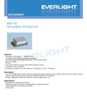
1. Product Overview
19-213 is a surface-mount device (SMD) LED designed specifically for modern compact electronic applications. It utilizes indium gallium nitride (InGaN) chip technology to produce a bright green light output. The core advantage of this component lies in its miniature size, which significantly reduces the footprint on the PCB (Printed Circuit Board), increases component assembly density, and contributes to the overall miniaturization of end-user equipment. Its lightweight structure makes it an ideal choice for applications where space and weight are constrained.
This LED is packaged on an 8mm carrier tape, wound onto a reel with a diameter of 7 inches, and is fully compatible with high-speed automated pick-and-place assembly equipment. This compatibility simplifies the manufacturing process for mass production.
1.1 Core Advantages and Target Market
The core advantages of the 19-213 SMD LED stem from its SMD package form and material compliance. It abandons the traditional lead frame, thereby achieving a more robust connection to the PCB and offering better performance in high-vibration environments. This product is classified as lead-free, complying with the EU's RoHS (Restriction of Hazardous Substances) directive and adhering to REACH (Registration, Evaluation, Authorisation and Restriction of Chemicals) regulations. Simultaneously, it is also halogen-free, with bromine (Br) and chlorine (Cl) content each below 900 ppm, and their sum below 1500 ppm, making it suitable for environmentally conscious designs.
Its target applications are diverse, primarily focusing on indicator lights and backlighting functions. Key markets include automotive interiors (e.g., dashboard and switch backlighting), communication equipment (e.g., indicator lights on telephones and fax machines), and consumer electronics (e.g., flat backlighting for LCDs, switches, and symbols). Its versatility also makes it suitable for a wide range of other indicator applications.
2. In-depth Technical Parameter Analysis
This section provides a detailed and objective interpretation of the key electrical, optical, and thermal parameters defined in the datasheet. Understanding these limit and typical values is crucial for reliable circuit design.
2.1 Absolute Maximum Ratings
Absolute maximum ratings define the stress limits that may cause permanent damage to the device. These are not normal operating conditions.
- Reverse Voltage (VR): 5V- Applying a reverse bias voltage exceeding 5V may cause immediate junction breakdown. The datasheet clearly states that this device is not designed for reverse operation; this rating is primarily for IR test conditions.
- Forward Current (IF): 25mA- The maximum DC current that can flow continuously through the LED. Exceeding this value will generate excessive heat, leading to accelerated luminous flux degradation or catastrophic failure.
- Peak Forward Current (IFP): 100mA- This is the maximum allowable pulse current, specified with a duty cycle of 1/10 and a frequency of 1kHz. It allows for higher brightness in a short period but must be used with precise timing control.
- Power Dissipation (Pd): 95mW- Maximum power that can be dissipated as heat, calculated as VF * IF. Careful thermal management of the PCB is required when operating near this limit.
- Electrostatic Discharge (ESD): 150V (Human Body Model)- This Human Body Model rating indicates the device has a moderate level of ESD sensitivity. Proper ESD handling procedures must be followed during assembly and operation to prevent latent or immediate failures.
- Operating Temperature (Topr): -40°C to +85°C- The ambient temperature range within which the device is guaranteed to operate according to its published specifications.
- Storage Temperature (Tstg): -40°C to +90°C- The temperature range for storage when the device is in a non-operating state.
- Tsol (Soldering Temperature)Two soldering profiles are specified: reflow soldering (peak temperature 260°C, duration not exceeding 10 seconds) and hand soldering (soldering iron tip temperature 350°C, contact time per termination not exceeding 3 seconds).
2.2 Electro-Optical Characteristics
Unless otherwise specified, these parameters are measured under standard test conditions of Ta=25°C and IF=5mA. They define the optical performance of the LED.
- Luminous intensity (Iv): 45 - 112 mcd (min - max)- The perceived brightness of the LED measured in millicandelas. The broad range indicates the use of a binning system (see Section 3 for details). A typical value is not explicitly given and falls somewhere within this range.
- Viewing Angle (2θ1/2): 120° (Typical)- The angular span at which the luminous intensity drops to half of its peak value. This is a very wide viewing angle, ideal for applications requiring visibility from off-axis positions.
- Peak Wavelength (λp): 518 nm (Typical)- Wavelength at which the spectral power distribution of the emitted light reaches its maximum value.
- Dominant Wavelength (λd): 520 - 535 nm- The wavelength of monochromatic light that can evoke the same perceived color as the LED's output. This is a key parameter for color specification and is also binned.
- Spectral Bandwidth (Δλ): 35 nm (Typical)- The width of the emission spectrum, measured at half the maximum power (Full Width at Half Maximum - FWHM). A value of 35nm is typical for InGaN green LEDs.
- Forward Voltage (VF): 2.70 - 3.20 V- The voltage drop across the LED when driven by a 5mA test current. This range is also subject to binning. The tolerance for this parameter is ±0.05V of the binned value.
- Reverse Current (IR): 50 μA (Max)- Maximum leakage current when the specified reverse voltage (5V) is applied.
3. Explanation of the Grading System
To ensure color and brightness consistency in production, LEDs are binned according to performance. 19-213 uses three independent binning parameters.
3.1 Luminous Intensity Grading
LEDs are divided into four bins (P1, P2, Q1, Q2) based on their luminous intensity measured at IF=5mA. The bin ranges are as follows: P1 (45.0-57.0 mcd), P2 (57.0-72.0 mcd), Q1 (72.0-90.0 mcd), and Q2 (90.0-112.0 mcd). The tolerance for the binning value is ±11%. Designers must select the appropriate bin to meet the brightness level required for their application.
3.2 Dominant Wavelength Binning
Color consistency is managed by dividing the dominant wavelength into three groups: X (520-525 nm), Y (525-530 nm), and Z (530-535 nm). The tolerance is ±1nm. This ensures all LEDs from the same batch produce a very similar green hue.
3.3 Forward Voltage Binning
The forward voltage is divided into five groups with a step of 0.1V: 29 (2.70-2.80V), 30 (2.80-2.90V), 31 (2.90-3.00V), 32 (3.00-3.10V), and 33 (3.10-3.20V). The tolerance is ±0.05V. Understanding the VF bin helps in designing more precise current-limiting circuits, especially when driving multiple LEDs in series.
4. Performance Curve Analysis
The datasheet includes several typical characteristic curves, which are crucial for understanding the behavior of LEDs under non-standard conditions.
4.1 Relationship between Relative Luminous Intensity and Ambient Temperature
The curve shows how light output decreases as ambient temperature (Ta) increases. Like all LEDs, the 19-213 experiences luminous flux depreciation with rising temperature. In applications where the LED or its environment may become hot, designers must account for this thermal derating to ensure sufficient brightness is maintained at the maximum operating temperature.
4.2 Relationship between Relative Luminous Intensity and Forward Current
This graph illustrates the nonlinear relationship between drive current and light output. While increasing the current boosts brightness, efficiency (lumens per watt) typically decreases at higher currents due to increased heat generation. It also shows that light output tends to saturate as the current approaches the maximum rated value.
4.3 Relationship between Forward Voltage and Forward Current (IV Curve)
IV curve shine tushen ƙirar da'ira. Yana nuna alaƙar ƙarfin lantarki da ƙarfin kunnawa a cikin diode. A wurin "karkatacciyar hanya" kusa da matsakaicin ƙarfin lantarki mai gaba, LED ta fara haskakawa sosai. Wannan lanƙwasa yana da mahimmanci don zaɓar hanyar da ta dace don iyakance ƙarfin kunnawa (misali, ƙimar juriya ko saitin mai tuƙi na ƙarfin kunnawa mai dorewa).
4.4 Radiation Pattern
The polar plot depicts the spatial distribution of light intensity. The 120° viewing angle of the 19-213 forms a broad, Lambertian-like emission pattern. This confirms its suitability for wide-area lighting and indicator applications requiring visibility from all angles.
5. Mechanical and Packaging Information
5.1 Package Dimensions
The datasheet provides a detailed two-dimensional drawing of the LED package, including key dimensions. Key measurements include overall length, width, height, pad size and location, and the position of the cathode identifier (typically a notch or green marking at one corner). All unspecified tolerances are ±0.1mm. This drawing is essential for creating the PCB pad pattern (footprint) in CAD software.
5.2 Polarity Identification
Correct polarity is crucial for operation. The package includes a visual marker to identify the cathode (-) terminal. Designers and assembly technicians must refer to the dimension drawing to correctly orient the component on the PCB.
6. Welding and Assembly Guide
Adhering to these guidelines is crucial for achieving reliable solder joints without damaging the LED.
6.1 Reflow Soldering Temperature Profile
Recommended lead-free reflow soldering temperature profile is provided. Key parameters include: preheat zone between 150-200°C, lasting 60-120 seconds; time above liquidus (217°C) 60-150 seconds; peak temperature not exceeding 260°C; maximum duration at peak temperature 10 seconds. Maximum heating rate 6°C/second, maximum cooling rate 3°C/second. Reflow soldering cycles should not exceed two.
6.2 Manual Soldering Precautions
If manual soldering is necessary, extra caution is required. The soldering iron tip temperature must be below 350°C, and contact time with each solder joint must not exceed 3 seconds. Use of a low-power soldering iron (≤25W) is recommended. Allow at least 2 seconds between soldering each joint for heat dissipation.
6.3 Storage and Moisture-proof Requirements
LEDs are packaged in moisture barrier bags with desiccant. The bag must not be opened until the components are ready for use. After opening, unused LEDs should be stored at ≤30°C and ≤60% relative humidity and used within 168 hours (7 days). If the storage time exceeds the specified limit or the desiccant indicates moisture absorption, baking at 60±5°C for 24 hours is required before use to prevent "popcorn" phenomenon during reflow soldering.
7. Packaging and Ordering Information
7.1 Reel Specifications
Components are supplied in embossed carrier tape, with dimensions specified in the datasheet. The tape is wound on standard 7-inch (178mm) diameter reels. Each reel contains 3000 pieces. Reel dimensions (hub diameter, flange diameter, width) are provided to ensure compatibility with automated assembly equipment.
7.2 Label Description
The reel label contains several key codes: P/N (Product Number), QTY (Quantity), CAT (Luminous Intensity Grade/Bin), HUE (Chromaticity/Dominant Wavelength Grade), REF (Forward Voltage Grade), and LOT No (Traceable Lot Number). Understanding this label is crucial for inventory control and ensuring the correct performance bin is used in production.
8. Application Design Considerations
8.1 Must use current limiting measures
The datasheet emphasizes that an external current-limiting resistor (or constant current driver) must be used. When the voltage slightly exceeds its forward voltage, the current through an LED increases exponentially and sharply. Without current limiting, even minor power supply voltage fluctuations can cause the current to exceed the maximum rating, leading to immediate failure.MustUse. When the voltage slightly exceeds its forward voltage, the current of an LED increases exponentially and sharply. Without current limiting, even minor power supply voltage fluctuations can cause the current to exceed the maximum rated value, leading to immediate failure.
8.2 Thermal management
Although the package itself dissipates heat, the primary thermal path is through the pads into the PCB copper layers. For applications operating in high ambient temperatures or near maximum current, PCBs with adequate thermal design, wider copper traces, or even dedicated thermal pads connected to a ground plane should be considered to aid heat dissipation.
8.3 Electrostatic Discharge (ESD) Protection
Given the 150V HBM ESD rating, incorporating basic ESD protection (e.g., using transient voltage suppression diodes or series resistors) on lines connected to the LED may be advisable, especially in environments prone to electrostatic discharge, particularly when the LED is user-accessible.
9. Technical Comparison and Differentiation
The 19-213 differentiates itself primarily through the combination of its 120° ultra-wide viewing angle and transparent resin. Many indicator LEDs use diffused resin to widen the viewing angle, but this reduces the axial peak intensity. The 19-213 achieves a wide viewing angle using transparent resin, which can provide higher perceived brightness directly on-axis while maintaining good off-axis visibility. Its full compliance with modern environmental regulations (RoHS, REACH, Halogen-Free) is also a standard yet essential requirement for most new designs.
10. Frequently Asked Questions (Based on Technical Parameters)
10.1 When using a 5V power supply, what resistance value should be selected?
The resistance value (R) depends on the desired forward current (IF) and the forward voltage (VF) of the specific LED bin. Use Ohm's law: R = (Power Supply Voltage - VF) / IF. For example, using a 5V supply, VF of 3.0V (Bin 31), and a target IF of 20mA: R = (5 - 3.0) / 0.020 = 100 ohms. Always calculate the resistor's power dissipation: P_resistor = (Power Supply Voltage - VF) * IF. In this example, P = 2V * 0.02A = 0.04W, so a standard 1/8W (0.125W) resistor is sufficient.
10.2 Can this LED be driven for dimming using a PWM signal?
可以,脉宽调制(PWM)是调光LED的绝佳方法。它通过快速开关LED来工作。感知亮度与占空比(LED开启时间的百分比)成正比。与模拟调光(降低电流)可能导致颜色偏移不同,PWM调光能保持LED的颜色一致性。确保PWM频率足够高(通常>100Hz)以避免可见闪烁。
10.3 Why are the storage and baking processes so important?
SMD packages absorb moisture from the atmosphere. During the high-temperature reflow soldering process, this trapped moisture rapidly vaporizes, creating steam pressure inside the package. This can lead to internal delamination, resin cracking, or bond wire failure—a phenomenon known as the "popcorn" effect. Moisture barrier packaging and baking procedures are designed to prevent this failure mode.
11. Practical Design and Usage Examples
11.1 Multi-LED Array for Panel Backlighting
To provide backlighting for small LCDs or switch panels, multiple 19-213 LEDs can be arranged in an array. Due to forward voltage binning, it is generally more reliable to connect the LEDs in parallel, each with its own individual current-limiting resistor, rather than in series. This configuration ensures that variations in VF among individual LEDs do not lead to uneven current distribution and inconsistent brightness. For larger arrays, constant-current driver ICs designed for multiple parallel LED channels will provide the most uniform and efficient solution.
11.2 Status Indicator Light Connected to the Microcontroller
When driving directly from a microcontroller GPIO pin, the pin's current source/sink capability must be checked. The limit for many MCU pins is 20-25mA, which matches the maximum for this LED very well. The circuit will consist of an LED and a series resistor, connected between the MCU pin and ground (for a current sink configuration) or VCC (for a current source configuration). The resistor value is calculated using the MCU's output voltage (e.g., 3.3V) and the LED's VF.
12. Brief Introduction to the Working Principle
19-213 LED is based on a semiconductor diode structure made of indium gallium nitride (InGaN). When a forward voltage exceeding the diode junction potential (approximately 2.7-3.2V) is applied, electrons and holes are injected into the active region of the semiconductor. When these charge carriers recombine, they release energy in the form of photons (light). The specific composition of the InGaN alloy determines the semiconductor's bandgap energy, which directly dictates the wavelength (color) of the emitted light. In this case, the alloy is tuned to produce photons in the green spectrum (520-535 nm). The transparent epoxy encapsulation protects the semiconductor chip, provides mechanical stability, and acts as a lens to shape the emitted light into a 120° viewing angle.
13. Technical Trends and Background
19-213 yana wakiltar fasaha mai cikakken kwarewa kuma ana amfani da ita sosai a kasuwar SMD LED. Hanyoyin da ake bi a wannan fanni suna ci gaba da tafiya zuwa ga wasu mahimman hanyoyi. Na farko, haɓaka ingancin haske (samar da ƙarin haske a kowace wutar lantarki) yana ci gaba da zama abin motsa jiki, wanda ke haɓaka ingancin makamashi. Na biyu, neman mafi girman tsaftar launi da cikar launi, musamman a cikin bakan kore, har yanzu yana aiki. Na uku, ƙananan ƙirar kunshe yana ci gaba, ƙananan siffofi fiye da 19-213 sun zama gama gari a cikin na'urori masu matuƙar ƙanƙanta. A ƙarshe, haɗawa wata hanya ce da ke girma, LED masu launuka daban-daban (RGB) ko LED masu haɗa da'irar sarrafawa (kamar I2C addressable LED) suna haɗa ayyuka da yawa zuwa cikin kunshe ɗaya, suna sauƙaƙe ƙira da haɗawa. 19-213, tare da amincinta, samuwa mai yawa, da bin ka'idoji, ya zama ginshiƙin ginin babban tsarin alamar nuni da aikace-aikacen haske.
Cikakken Bayani Kan Kalmomin Ƙayyadaddun LED
Cikakken Bayani Kan Kalmomin Fasahar LED
I. Core Indicators of Photoelectric Performance
| Terminology | Unit/Representation | Popular Explanation | Why It Is Important |
|---|---|---|---|
| Luminous Efficacy | lm/W (lumens per watt) | The luminous flux emitted per watt of electrical energy, the higher the more energy-efficient. | Directly determines the energy efficiency class and electricity cost of the luminaire. |
| Luminous Flux | lm (lumen) | The total amount of light emitted by a light source, commonly known as "brightness". | Determine if the lamp is bright enough. |
| Viewing Angle | ° (degree), such as 120° | The angle at which light intensity drops to half, determining the beam's width. | Affects the illumination range and uniformity. |
| Color Temperature (CCT) | K (Kelvin), e.g., 2700K/6500K | The warmth or coolness of light color; lower values are yellowish/warm, higher values are whitish/cool. | Determines the lighting atmosphere and suitable application scenarios. |
| Color Rendering Index (CRI / Ra) | No unit, 0–100 | The ability of a light source to reproduce the true colors of objects, Ra≥80 is recommended. | Affects color fidelity, used in high-demand places such as shopping malls and art galleries. |
| Color Tolerance (SDCM) | MacAdam Ellipse Steps, e.g., "5-step" | Quantitative indicator of color consistency, the smaller the step number, the more consistent the color. | Ensure no color difference among the same batch of luminaires. |
| Dominant Wavelength | nm (nanometer), e.g., 620nm (Red) | The wavelength value corresponding to the color of a colored LED. | Determine the hue of monochromatic LEDs such as red, yellow, and green. |
| Spectral Distribution | Wavelength vs. Intensity Curve | It shows the intensity distribution of light emitted by an LED across various wavelengths. | It affects color rendering and color quality. |
Two, Electrical Parameters
| Terminology | Symbol | Popular Explanation | Design Considerations |
|---|---|---|---|
| Forward Voltage | Vf | Minimum voltage required to turn on an LED, similar to a "starting threshold". | The driving power supply voltage must be ≥ Vf, and the voltage adds up when multiple LEDs are connected in series. |
| Forward Current | If | The current value that allows the LED to emit light normally. | A cikin yawancin lokuta ana amfani da tuƙi mai tsayayyen kwarara, kwararar wutar lantarki tana ƙayyadaddun haske da tsawon rayuwa. |
| Matsakaicin ƙarfin wutar lantarki na bugun jini (Pulse Current) | Ifp | Peak current that can be withstood in a short time, used for dimming or flashing. | Pulse width and duty cycle must be strictly controlled, otherwise overheating damage will occur. |
| Reverse Voltage | Vr | The maximum reverse voltage that an LED can withstand; exceeding it may cause breakdown. | The circuit must be protected against reverse connection or voltage surges. |
| Thermal Resistance | Rth (°C/W) | The resistance to heat flow from the chip to the solder joint. A lower value indicates better heat dissipation. | High thermal resistance requires a more robust thermal design; otherwise, the junction temperature will increase. |
| Electrostatic Discharge Immunity (ESD Immunity) | V (HBM), such as 1000V | Anti-static strike capability, the higher the value, the less susceptible to damage from static electricity. | Anti-static measures must be implemented during production, especially for high-sensitivity LEDs. |
III. Thermal Management and Reliability
| Terminology | Key Metrics | Popular Explanation | Impact |
|---|---|---|---|
| Junction Temperature | Tj (°C) | The actual operating temperature inside the LED chip. | For every 10°C reduction, the lifespan may double; excessively high temperatures lead to lumen depreciation and color shift. |
| Lumen Depreciation | L70 / L80 (hours) | The time required for brightness to drop to 70% or 80% of its initial value. | Directly defines the "service life" of an LED. |
| Lumen Maintenance | % (e.g., 70%) | Percentage of remaining brightness after a period of use. | Characterizes the ability to maintain brightness after long-term use. |
| Color Shift | Δu′v′ or MacAdam Ellipse | The degree of color change during use. | Affects the color consistency of the lighting scene. |
| Thermal Aging | Material performance degradation | Degradation of packaging materials due to long-term high temperature. | May lead to decreased brightness, color shift, or open-circuit failure. |
IV. Encapsulation and Materials
| Terminology | Common Types | Popular Explanation | Characteristics and Applications |
|---|---|---|---|
| Package Type | EMC, PPA, Ceramic | Material casing yang melindungi chip dan menyediakan antarmuka optik serta termal. | EMC tahan panas baik, biaya rendah; keramik pendinginan unggul, umur panjang. |
| Struktur chip | Front-side, Flip Chip | Chip Electrode Layout Method. | Flip-chip offers better heat dissipation and higher luminous efficacy, suitable for high-power applications. |
| Phosphor coating | YAG, Silicate, Nitride | Covered on the blue light chip, partially converted into yellow/red light, mixed into white light. | Different phosphors affect luminous efficacy, color temperature, and color rendering. |
| Lens/Optical Design | Flat, Microlens, Total Internal Reflection | Optical structure on the encapsulation surface, controlling light distribution. | Determines the emission angle and light distribution curve. |
V. Quality Control and Binning
| Terminology | Binning Content | Popular Explanation | Purpose |
|---|---|---|---|
| Luminous Flux Binning | Codes such as 2G, 2H | Grouped by brightness level, each group has a minimum/maximum lumen value. | Ensure uniform brightness for products within the same batch. |
| Voltage binning | Codes such as 6W, 6X | Grouped by forward voltage range. | Facilitates driver power matching and improves system efficiency. |
| Color Grading | 5-step MacAdam Ellipse | Group by color coordinates to ensure colors fall within a minimal range. | Ensure color consistency to avoid uneven colors within the same luminaire. |
| Color temperature binning | 2700K, 3000K, etc. | Grouped by color temperature, each group has a corresponding coordinate range. | To meet the color temperature requirements of different scenarios. |
VI. Testing and Certification
| Terminology | Standard/Test | Popular Explanation | Meaning |
|---|---|---|---|
| LM-80 | Lumen Maintenance Test | Long-term illumination under constant temperature conditions, recording brightness attenuation data. | Used to estimate LED lifetime (combined with TM-21). |
| TM-21 | Standard for Life Projection | Projecting the actual service life based on LM-80 data. | Provide scientific life prediction. |
| IESNA standard | Standard of the Illuminating Engineering Society | Covers optical, electrical, and thermal testing methods. | Industry-recognized testing basis. |
| RoHS / REACH | Environmental certification | Ensure the product does not contain harmful substances (e.g., lead, mercury). | Conditions for market access to the international market. |
| ENERGY STAR / DLC | Energy Efficiency Certification | Energy efficiency and performance certification for lighting products. | Yawan da ake amfani da shi a cikin sayayyar gwamnati da ayyukan tallafi, don haɓaka gasar kasuwa. |