Table of Contents
- 1. Product Overview
- 1.1 Core Advantages and Product Positioning
- 1.2 Target Market and Applications
- 2. Technical Specifications and Objective Interpretation
- 2.1 Absolute Maximum Ratings
- 2.2 Photoelectric Characteristics (Ta=25°C)
- 3. Binning System Description
- 3.1 Luminous Intensity Binning
- 3.2 Dominant Wavelength Binning
- 3.3 Forward Voltage Binning
- 4. Performance Curve Analysis
- 4.1 Forward Current vs. Forward Voltage (I-V Curve)
- 4.2 Relative Luminous Intensity vs. Ambient Temperature
- 4.3 Relative Luminous Intensity vs. Forward Current
- 4.4 Forward Current Derating Curve
- 4.5 Spectral Distribution
- 4.6 Radiation Pattern
- 5. Mechanical and Packaging Information
- 5.1 Package Dimensions
- 5.2 Polarity Identification
- 6. Welding and Assembly Guide
- 6.1 Reflow Soldering Temperature Profile
- 6.2 Manual Soldering Instructions
- 6.3 Storage and Moisture Sensitivity
- 6.4 Key Considerations
- 7. Packaging and Ordering Information
- 7.1 Standard Packaging
- 7.2 Moisture-Proof Packaging
- 7.3 Label Instructions
- 8. Application Suggestions and Design Considerations
- 8.1 Driver Circuit Design
- 8.2 Thermal Management
- 8.3 Optical Design
- 9. Compliance and Environmental Specifications
- 10. Technical Comparison and Differentiation
- 11. Frequently Asked Questions (FAQ)
- 12. Design Use Case Studies
- 13. Introduction to Working Principles
- 14. Technology Trends and Background
1. Product Overview
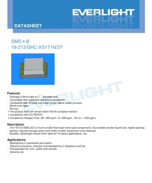
19-213/GHC-XS1T1N/3T is a surface-mount device (SMD) LED, specifically designed for modern compact electronic applications. Compared to traditional lead-frame LEDs, it represents a significant technological advancement, offering substantial advantages in circuit board space utilization, assembly efficiency, and final product miniaturization.
1.1 Core Advantages and Product Positioning
The primary advantage of this LED lies in its miniature package size, which directly contributes to smaller printed circuit board (PCB) designs, higher component assembly density, and reduced storage space requirements. Its lightweight structure makes it an ideal choice for application scenarios where weight is a critical factor. This product is positioned as a reliable, versatile indicator light and backlight solution suitable for automated high-volume production.
1.2 Target Market and Applications
This device targets a wide range of industries requiring compact and efficient lighting. The main application areas include:
- Automotive Interior:Backlighting for dashboard instruments, switches, and control panels.
- Telecommunications Equipment:Status indicators and keyboard backlighting in telephones, fax machines, and other communication equipment.
- Consumer Electronics:Planar backlighting, switch illumination, and symbol indicators for Liquid Crystal Displays (LCD).
- General Domain:Any application requiring a small, bright green indicator light.
2. Technical Specifications and Objective Interpretation
This section provides a detailed and objective analysis of the LED's electrical, optical, and thermal characteristics as defined in the datasheet.
2.1 Absolute Maximum Ratings
These ratings define the stress limits that may cause permanent damage to the device. Operation at or beyond these limits is not guaranteed.
- Reverse Voltage (VR):5V. Exceeding this voltage under reverse bias may cause immediate junction breakdown.
- Continuous Forward Current (IF):25mA. The maximum DC current for ensuring long-term reliable operation.
- Peak Forward Current (IFP):100mA (duty cycle 1/10, frequency 1kHz). Suitable for pulse operation, not for DC.
- Power dissipation (Pd):95mW. The maximum power that the package can dissipate without exceeding its thermal limits.
- Electrostatic Discharge (ESD):150V (Human Body Model). Indicates moderate sensitivity; standard ESD precautions must be observed.
- Operating and Storage Temperature:-40°C to +85°C (operating), -40°C to +90°C (storage). Suitable for industrial and extended temperature range applications.
- Soldering temperature:Reflow soldering: up to 260°C, maximum 10 seconds. Hand soldering: up to 350°C per pin, maximum 3 seconds.
2.2 Photoelectric Characteristics (Ta=25°C)
These are typical performance parameters under standard test conditions.
- Luminous intensity (Iv):180-360 mcd (at IF=20mA condition). This defines the perceived brightness. The wide range indicates the use of a binning system (see Section 3).
- Viewing angle (2θ1/2):120 degrees (typical). This wide viewing angle provides a broad, uniform illumination pattern, suitable for backlights and indicator lights viewed from different angles.
- Peak Wavelength (λp):518 nm (typical). The spectral peak of the emitted light, located in the bright green region.
- Dominant Wavelength (λd):515-530 nm. Defines the perceived hue. This range is also affected by binning.
- Spectral Bandwidth (Δλ):35 nm (typical). The width of the emission spectrum at half the peak intensity.
- Forward Voltage (VF):2.70-3.70 V (at IF=20mA condition). Important for drive circuit design and power consumption calculation. This parameter is binned.
- Reverse current (IR):< 50 µA(在 VR=5V condition). Low leakage current specification.
Key considerations:The datasheet explicitly states that this deviceis not designed for reverse operation.. The reverse voltage rating is only for leakage current testing.
3. Binning System Description
To ensure consistency in mass production, LEDs are sorted (binned) based on key parameters. The 19-213 employs a three-dimensional binning system.
3.1 Luminous Intensity Binning
Gear: S1 (180-225 mcd), S2 (225-285 mcd), T1 (285-360 mcd). Designers must select the appropriate gear to meet the brightness required for their application, considering the ±11% tolerance within each gear.
3.2 Dominant Wavelength Binning
Gear: W (515-520 nm), X (520-525 nm), Y (525-530 nm). This ensures color consistency among multiple LEDs in an array. The tolerance within each gear is ±1 nm.
3.3 Forward Voltage Binning
Bin: 10 (2.70-2.90V), 11 (2.90-3.10V), 12 (3.10-3.30V), 13 (3.30-3.50V), 14 (3.50-3.70V). Selecting LEDs from the same VFbin helps achieve uniform current distribution and predictable power supply requirements when connected in parallel. The bin content tolerance is ±0.1V.
4. Performance Curve Analysis
The datasheet provides several characteristic curves necessary for understanding the device's behavior under different conditions.
4.1 Forward Current vs. Forward Voltage (I-V Curve)
This curve illustrates the exponential relationship between current and voltage. For a typical LED, a slight increase in voltage beyond the turn-on point results in a significant increase in current. This highlights the necessity of using a current-limiting resistor or constant-current driver to prevent thermal runaway.
4.2 Relative Luminous Intensity vs. Ambient Temperature
Light output decreases as ambient temperature rises. This curve is crucial for applications operating in high-temperature environments, such as inside automotive dashboards. Designers must derate the expected brightness based on the operating temperature.
4.3 Relative Luminous Intensity vs. Forward Current
Light output is typically proportional to forward current, but the relationship is not perfectly linear, especially at higher currents. Efficiency may decline at extremely high currents due to increased thermal effects.
4.4 Forward Current Derating Curve
This graph defines the maximum allowable continuous forward current as a function of ambient temperature. As temperature increases, the maximum safe current decreases to prevent exceeding the junction temperature limit and ensure long-term reliability.
4.5 Spectral Distribution
The curve shows a single peak centered at 518 nm, confirming a monochromatic green light output. The 35 nm bandwidth indicates that the color is a relatively pure green.
4.6 Radiation Pattern
Illustrates the spatial distribution of light intensity, confirming a 120-degree viewing angle with a typical Lambertian or near-Lambertian emission pattern.
5. Mechanical and Packaging Information
5.1 Package Dimensions
The datasheet includes detailed dimensional drawings. Key features include overall length, width, height, pad layout, and polarity indicator (typically a notch or marked cathode). Unless otherwise specified, the standard tolerance for all dimensions is ±0.1mm. Strict adherence to the recommended pad layout is crucial for reliable soldering and proper alignment during reflow.
5.2 Polarity Identification
Polarity must be connected correctly. The package contains a visual indicator (e.g., a green dot, a notch, or a cathode mark) to identify the cathode terminal. Reverse-biasing the LED may damage it.
6. Welding and Assembly Guide
Proper handling and soldering are crucial for yield rate and reliability.
6.1 Reflow Soldering Temperature Profile
Specifies the lead-free reflow soldering temperature profile:
- Preheating:150-200°C, for 60-120 seconds.
- Time Above Liquidus (TAL):>217°C,持续60-150秒。
- Peak temperature:Maximum 260°C, kana da 10 dakika.
- Heating/cooling rate:Heating: Maximum 3°C/sec. Cooling: Maximum 6°C/sec.
6.2 Manual Soldering Instructions
If manual welding must be performed:
- 使用烙铁头温度<350°C的烙铁。
- 每个引脚焊接时间限制在3秒以内。使用额定功率<25W的烙铁。焊接每个引脚之间至少间隔2秒。The datasheet warns that damage often occurs during manual soldering.
6.3 Storage and Moisture Sensitivity
This component is sensitive to humidity.
- Before use:Do not open the moisture barrier bag until ready for use.
- After opening:Please use within 168 hours (7 days). Unused components should be stored in an environment of ≤30°C and ≤60% relative humidity.
- Re-baking:If exposure time exceeds the specified limit or the desiccant indicator shows moisture absorption, bake at 60±5°C for 24 hours.
6.4 Key Considerations
- Overcurrent Protection:External current limiting resistor isMandatory requirement. A slight voltage change may cause a significant current change, leading to immediate failure.
- Mechanical stress:Avoid applying stress to the LED body during soldering or final application. Do not twist the PCB after assembly.
- Rework:Rework is not recommended. If absolutely necessary, use a dual-tip soldering iron to simultaneously heat both pins to avoid thermal stress. Verify device functionality after rework.
7. Packaging and Ordering Information
7.1 Standard Packaging
The device is supplied in 8mm carrier tape, wound on 7-inch diameter reels, compatible with standard automated placement equipment. Each reel contains 3000 units.
7.2 Moisture-Proof Packaging
To extend shelf life, the reel is packaged in an aluminum moisture barrier bag with desiccant and humidity indicator card.
7.3 Label Instructions
The reel label contains key information:
- CPN: Customer Part Number.
- P/N: Manufacturer Part Number (e.g., 19-213/GHC-XS1T1N/3T).
- QTY: Quantity on reel.
- CAT: Luminous intensity bin code (e.g., S1, T1).
- HUE: Chromaticity/Dominant wavelength bin code (e.g., W, X, Y).
- REF: Forward voltage bin code (e.g., 10, 11, 12).
- LOT No.: Traceable batch number.
8. Application Suggestions and Design Considerations
8.1 Driver Circuit Design
Always drive this LED with a constant current source, or use a series resistor calculated based on the worst-case forward voltage (maximum VFbin) and the supply voltage to ensure the current never exceeds 25mA DC. For example, with a 5V supply and a VFof 3.7V, a series resistor of at least (5V - 3.7V) / 0.025A = 52 ohms is required. For a safety margin, using a higher resistance value is recommended.
8.2 Thermal Management
Although the package is small, effective thermal management on the PCB is very important for extending lifespan and maintaining brightness. Use sufficient copper area connected to the thermal pad (if available) or anode/cathode traces to dissipate heat, especially when operating near maximum current or at high ambient temperatures.
8.3 Optical Design
120-degree viewing angle and transparent resin make this LED suitable for wide-angle indicator lights. For focused light or specific beam patterns, secondary optical elements (lenses, light guides) are required. Transparent resin provides the highest light output but may cause visible "hot spots"; diffused resin alternatives (not this model) are more suitable for uniform illumination.
9. Compliance and Environmental Specifications
This product complies with multiple key international standards, simplifying its use in the global market:
- RoHS compliant:Does not contain restricted hazardous substances such as lead, mercury, cadmium.
- EU REACH compliant:Compliance with the Registration, Evaluation, Authorisation and Restriction of Chemicals regulation.
- Halogen-free:符合严格限制:溴(Br)< 900 ppm,氯(Cl)< 900 ppm,Br+Cl < 1500 ppm。这对于减少火灾时的有毒排放物很重要。
- Lead-free:Both the soldering surface treatment and materials are lead-free.
10. Technical Comparison and Differentiation
Compared to older through-hole LED technology, this SMD LED offers:
- Size reduction:Significant size reduction, achieving miniaturization.
- Manufacturing efficiency:Compatible with fully automated SMT assembly lines, reducing labor costs and improving placement speed and accuracy.
- Performance:Typically provides a better thermal path to the PCB than many through-hole designs, potentially improving service life under high current.
11. Frequently Asked Questions (FAQ)
Q: Can I drive this LED directly from a 3.3V or 5V microcontroller pin?A: No. You must use a series current-limiting resistor. The forward voltage is approximately 3V, and a GPIO pin cannot safely source/sink 20mA while controlling the voltage drop. Please use a transistor or a dedicated LED driver.
Q: Why is the luminous intensity range so wide (180-360 mcd)?A: This is the total production range. Devices are sorted into specific bins (S1, S2, T1). The desired bin must be specified when ordering to ensure brightness consistency.
Q: The datasheet says "Do not open the packaging bag before use." What happens if it is opened?A: Moisture may be absorbed by the plastic encapsulation. During the reflow soldering process, this trapped moisture can rapidly expand ("popcorn effect"), leading to internal delamination and cracking, which can cause immediate or latent failures.
Q: Can I use it for outdoor applications?A: The operating temperature range (-40°C to +85°C) supports many outdoor environments. However, prolonged exposure to UV and weather may degrade the resin. For harsh outdoor use, LEDs with specially formulated UV-resistant encapsulation materials are recommended.
12. Design Use Case Studies
Scenario: Designing a status indicator panel for an industrial controller. Requirements:Multiple green LEDs are used to indicate "System Ready", "Communication Active", etc. Uniform brightness and color are crucial for user perception.
Design Steps:
- Gear Selection:To ensure consistency, specify a single, strict bin for all LEDs: for example, luminous intensity bin T1 (285-360 mcd), dominant wavelength bin X (520-525 nm), forward voltage bin 12 (3.10-3.30V). This guarantees that all LEDs will behave very similarly.
- Circuit Design:Use a constant-current LED driver IC capable of driving multiple channels. This provides identical current to each LED, unaffected by minor variations in VFensuring perfect brightness matching. Alternatively, if using one resistor per LED, base the calculation on the highest V within the bin.F(3.30V) Calculate the resistor value to ensure no LED is overdriven.
- PCB Layout:Place LEDs in a consistent orientation. Include sufficient copper pour area connected to the cathode pads to aid heat dissipation, as the panel may be illuminated continuously.
- Assembly:Operate strictly according to the specified reflow soldering temperature profile. Keep the reel sealed before loading it into the SMT feeder to comply with Moisture Sensitivity Level (MSL) requirements.
13. Introduction to Working Principles
This LED is based on an indium gallium nitride (InGaN) semiconductor chip. When a forward voltage exceeding the diode's turn-on threshold (VF) is applied, electrons and holes are injected into the active region of the semiconductor junction. When these charge carriers recombine, they release energy in the form of photons (light). The specific composition of the InGaN material determines the wavelength (color) of the emitted light; in this case, it is tuned to produce a bright green light with a peak at 518 nm. The transparent epoxy encapsulation protects the delicate semiconductor chip, provides mechanical stability, and acts as a primary lens to shape the initial light output pattern.
14. Technology Trends and Background
19-213 LED represents a mature and widely adopted SMD LED technology. Current LED development trends associated with this type of component include:
- Efficiency Improvement:Continuous improvements in epitaxial growth and chip design have led to higher luminous efficacy (more light output per watt of electrical input), enabling brighter indicator lights or lower power consumption.
- Miniaturization:The pursuit of smaller devices continues, with reduced package sizes (e.g., 0402, 0201 metric) becoming common in space-constrained applications, albeit often with trade-offs in light output and thermal performance.
- Reliability Enhancement:Improvements in packaging materials and die-attach technologies continue to extend operational lifespan and resistance to thermal cycling and humidity.
- Integrated Solutions:A broader trend involves integrating control electronics (current drivers, PWM controllers) directly with the LED chip into more complex modules, thereby simplifying circuit design for end users.
Detailed Explanation of LED Specification Terminology
Complete Explanation of LED Technical Terminology
I. Core Indicators of Photoelectric Performance
| Terminology | Unit/Representation | Layman's Explanation | Why is it important |
|---|---|---|---|
| Luminous Efficacy | lm/W | The luminous flux emitted per watt of electrical power; the higher the value, the more energy-efficient. | It directly determines the energy efficiency rating and electricity cost of the luminaire. |
| Luminous Flux | lm (lumen) | The total amount of light emitted by a light source, commonly known as "brightness". | Determines whether the luminaire is bright enough. |
| Viewing Angle | ° (degree), such as 120° | The angle at which light intensity drops to half, determining the beam width. | Affects the illumination range and uniformity. |
| Color Temperature (CCT) | K (Kelvin), e.g., 2700K/6500K | The color temperature of light: lower values are yellowish/warm, higher values are whitish/cool. | Determines the lighting ambiance and suitable application scenarios. |
| Color Rendering Index (CRI / Ra) | Unitless, 0–100 | The ability of a light source to reproduce the true colors of objects, with Ra≥80 being preferable. | Affects color fidelity, used in high-demand places such as shopping malls and art galleries. |
| Color tolerance (SDCM) | MacAdam ellipse steps, such as "5-step" | A quantitative metric for color consistency; a smaller step number indicates better color consistency. | Ensure no color variation among luminaires from the same batch. |
| Dominant Wavelength | nm (nanometer), e.g., 620nm (red) | The wavelength values corresponding to the colors of colored LEDs. | Determines the hue of monochromatic LEDs such as red, yellow, and green. |
| Spectral Distribution | Wavelength vs. Intensity curve | Shows the intensity distribution of light emitted by an LED at various wavelengths. | Affects color rendering and color quality. |
II. Electrical Parameters
| Terminology | Symbol | Layman's Explanation | Design Considerations |
|---|---|---|---|
| Forward Voltage (Forward Voltage) | Vf | Voltage ya chini inayohitajika kuwasha LED, kama "kizingiti cha kuanzisha". | Voltage ya chanzo cha usukumaji lazima iwe ≥ Vf, voltage inajumlishwa wakati LED nyingi zimeunganishwa mfululizo. |
| Forward Current | If | The current value that makes the LED emit light normally. | Constant current drive is often used, as the current determines brightness and lifespan. |
| Maximum Pulse Current | Ifp | Peak current that can be withstood for a short period of time, used for dimming or flashing. | Pulse width and duty cycle must be strictly controlled, otherwise overheating damage will occur. |
| Reverse Voltage | Vr | Maximum reverse voltage an LED can withstand; exceeding it may cause breakdown. | Reverse connection or voltage surges must be prevented in the circuit. |
| Thermal Resistance | Rth (°C/W) | The resistance to heat flow from the chip to the solder joint. A lower value indicates better heat dissipation. | High thermal resistance requires a stronger heat dissipation design, otherwise the junction temperature will increase. |
| Electrostatic Discharge Immunity (ESD Immunity) | V (HBM), such as 1000V | Electrostatic discharge immunity, higher value indicates greater resistance to electrostatic damage. | Anti-static measures must be implemented during production, especially for high-sensitivity LEDs. |
III. Thermal Management and Reliability
| Terminology | Key Indicators | Layman's Explanation | Impact |
|---|---|---|---|
| Junction Temperature | Tj (°C) | The actual operating temperature inside the LED chip. | For every 10°C reduction, the lifespan may double; excessively high temperatures lead to lumen depreciation and color shift. |
| Lumen Depreciation | L70 / L80 (hours) | The time required for the brightness to drop to 70% or 80% of its initial value. | Directly define the "service life" of an LED. |
| Lumen Maintenance | % (e.g., 70%) | The percentage of remaining brightness after a period of use. | Characterizes the ability to maintain brightness after long-term use. |
| Color Shift | Δu′v′ or MacAdam Ellipse | The degree of color change during use. | Affects the color consistency of the lighting scene. |
| Thermal Aging | Material performance degradation | Degradation of packaging materials due to prolonged high temperature. | May lead to decreased brightness, color shift, or open-circuit failure. |
IV. Packaging and Materials
| Terminology | Common Types | Layman's Explanation | Features and Applications |
|---|---|---|---|
| Package Type | EMC, PPA, Ceramic | The housing material that protects the chip and provides optical and thermal interfaces. | EMC offers good heat resistance and low cost; ceramics provide superior heat dissipation and long lifespan. |
| Chip Structure | Face-up, Flip Chip (Flip Chip) | Chip Electrode Arrangement Method. | Flip-chip offers better heat dissipation and higher luminous efficacy, suitable for high-power applications. |
| Phosphor coating | YAG, silicate, nitride | Covered on the blue light chip, partially converted into yellow/red light, mixed into white light. | Different phosphors affect luminous efficacy, color temperature, and color rendering. |
| Lens/Optical Design | Flat, microlens, total internal reflection | Optical structure of the encapsulation surface, controlling light distribution. | Determines the light emission angle and light distribution curve. |
V. Quality Control and Binning
| Terminology | Grading Content | Layman's Explanation | Purpose |
|---|---|---|---|
| Luminous flux binning | Codes such as 2G, 2H | Grouped by brightness level, each group has a minimum/maximum lumen value. | Ensure consistent brightness within the same batch of products. |
| Voltage binning | Codes such as 6W, 6X | Group by forward voltage range. | Facilitates driver power matching and improves system efficiency. |
| Color binning | 5-step MacAdam ellipse | Group by color coordinates, ensuring colors fall within an extremely narrow range. | Ensure color consistency to avoid uneven colors within the same luminaire. |
| Color temperature binning | 2700K, 3000K, etc. | Group by color temperature, each group has a corresponding coordinate range. | Meet the color temperature requirements of different scenarios. |
VI. Testing and Certification
| Terminology | Standard/Test | Layman's Explanation | Meaning |
|---|---|---|---|
| LM-80 | Lumen Maintenance Test | Long-term operation under constant temperature conditions, recording brightness attenuation data. | Used to estimate LED lifetime (combined with TM-21). |
| TM-21 | Lifetime projection standard | Estimating lifespan under actual operating conditions based on LM-80 data. | Providing scientific lifespan prediction. |
| IESNA standard | Illuminating Engineering Society Standard | Covers optical, electrical, and thermal test methods. | Industry-recognized testing basis. |
| RoHS / REACH | Environmental certification. | Ensure products are free from harmful substances (e.g., lead, mercury). | Entry requirements for the international market. |
| ENERGY STAR / DLC | Energy Efficiency Certification | Energy efficiency and performance certification for lighting products. | Commonly used in government procurement and subsidy programs to enhance market competitiveness. |