Table of Contents
- 1. Product Overview
- 1.1 Core Features and Advantages
- 1.2 Target Applications and Market
- 2. Technical Parameters: In-depth and Objective Analysis
- 2.1 Absolute Maximum Ratings
- 2.2 Photoelectric Characteristics
- 3. Binning System Description
- 3.1 Luminous Flux Binning
- 3.2 Forward Voltage Binning
- 3.3 Dominant Wavelength Binning
- 4. Performance Curve Analysis
- 4.1 Spectral Distribution
- 4.2 Typical Photoelectric Characteristic Curves
- 5. Mechanical and Packaging Information
- 5.1 Package Dimensions
- 5.2 Polarity Marking
- 6. Welding and Assembly Guide
- 6.1 Reflow Soldering Parameters
- 6.2 Storage and Handling Precautions
- 7. Packaging and Ordering Information
- 7.1 Moisture-proof packaging
- 7.2 Label instructions
- 7.3 Reel and Carrier Tape Dimensions
- 8. Application Suggestions and Design Considerations
- 8.1 Iyakance Gudu da Zane na Mai Turawa
- 8.2 Thermal Management
- 9. Reliability and Quality Assurance
- 10. Frequently Asked Questions (Based on Technical Parameters)
- 10.1 What is the difference between luminous flux binning and dominant wavelength binning?
- 10.2 How to interpret the forward current vs. soldering temperature graph (Figure 5)?
- 10.3 What does "workshop life" mean? Why is it important?
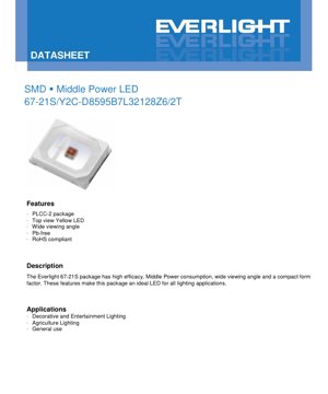
1. Product Overview
This document details the specifications of a medium-power SMD LED in PLCC-2 package emitting yellow light. Designed for general lighting applications, it offers a good balance of performance, efficiency, and compact size. The device features a wide viewing angle, is manufactured with lead-free materials, complies with RoHS standards, and is suitable for modern electronic assembly processes.
1.1 Core Features and Advantages
The primary advantages of this LED are its high luminous efficacy and medium-power characteristics, enabling efficient operation in various lighting scenarios. The compact PLCC-2 form factor facilitates easy integration into PCB designs, while the 120-degree wide viewing angle ensures uniform light distribution. Its compliance with lead-free and RoHS directives aligns with global environmental regulations.
1.2 Target Applications and Market
This LED is designed as a versatile component suitable for multiple lighting fields. Its primary application areas include decorative and entertainment lighting, which demand high color and brightness consistency. It is also well-suited for agricultural lighting systems. Furthermore, its versatility makes it a reliable choice for indicator lights, backlighting, and other common illumination tasks in consumer and industrial electronics.
2. Technical Parameters: In-depth and Objective Analysis
This section provides a detailed and objective analysis of the device's operational limits and performance characteristics under specified test conditions.
2.1 Absolute Maximum Ratings
Absolute maximum ratings define the stress limits that may cause permanent damage to the device. These ratings are specified at a soldering point temperature (T_Soldering) of 25°C. The continuous forward current (I_F) must not exceed 70 mA. For pulse operation, the permissible peak forward current (I_FP) is 140 mA under conditions of a duty cycle of 1/10 and a pulse width of 10 ms. The maximum power dissipation (P_d) is 200 mW. The device can operate within an ambient temperature (T_opr) range of -40°C to +85°C and can be stored (T_stg) at temperatures from -40°C to +100°C. The thermal resistance from junction to soldering point (R_th J-S) is 50 °C/W, and the maximum allowable junction temperature (T_j) is 115°C. Soldering must follow strict thermal profiles: reflow soldering up to 260°C for a maximum of 10 seconds; or hand soldering up to 350°C for a maximum of 3 seconds. An important note emphasizes that the product is sensitive to electrostatic discharge (ESD), requiring appropriate handling precautions.
2.2 Photoelectric Characteristics
Photometric and electrical characteristics are measured at a solder point temperature T_Soldering = 25°C and a test current (I_F) of 60 mA (representing the typical operating point). The typical luminous flux (I_v) ranges from 8.5 lm (minimum) to 13.0 lm (maximum). The forward voltage (V_F) is typically between 2.1 V and 2.8 V. The viewing angle (2θ_1/2), defined as the full width at half maximum intensity, is 120 degrees. A maximum reverse current (I_R) of 50 µA is guaranteed when a reverse voltage (V_R) of 5V is applied. Important tolerances are noted: luminous flux tolerance is ±11%, and forward voltage tolerance around its bin value is ±0.1V.
3. Binning System Description
To ensure consistency across production batches, LEDs are sorted into different bins based on key performance parameters. This allows designers to select components that meet the specific brightness and electrical characteristic requirements of their application.
3.1 Luminous Flux Binning
Ana rarraba fitowar haske zuwa lambobin nau'ikan nau'ikan da yawa (B7, B8, B9, L1, L2, L3), kowace lamba tana bayyana takamaiman ƙananan da manyan ƙimar ƙarfin haske da aka auna a I_F=60mA. Misali, nau'in B7 ya ƙunshi 8.5 zuwa 9.0 lm, yayin da nau'in L3 ya ƙunshi 12.0 zuwa 13.0 lm. Matsakaicin ƙarfin haske gabaɗaya yana da ƙarancin ±11%.
3.2 Forward Voltage Binning
The forward voltage is binned into codes from 28 to 34, with each code representing a 0.1V step. Code 28 covers 2.1V to 2.2V, and code 34 covers 2.7V to 2.8V. The tolerance of the forward voltage relative to the binning range is ±0.1V.
3.3 Dominant Wavelength Binning
Yellow light is defined by its dominant wavelength. Two bin codes are specified: Y52 corresponds to a dominant wavelength range of 585 nm to 590 nm, and Y53 corresponds to 590 nm to 595 nm. The measurement tolerance for dominant/peak wavelength is ±1 nm.
4. Performance Curve Analysis
Graphical data reveals the behavior of LEDs under various operating conditions, which is crucial for robust circuit design and thermal management.
4.1 Spectral Distribution
The provided spectral curve shows the relative luminous intensity across a wavelength range from approximately 540 nm to 640 nm. The curve peaks in the yellow region (around 585-595 nm), confirming the dominant wavelength binning, with minimal emission in other parts of the visible spectrum.
4.2 Typical Photoelectric Characteristic Curves
The diagram illustrates several key relationships: Figure 1 shows the forward voltage shift decreasing linearly as the junction temperature rises from 25°C to 115°C. Figure 2 depicts the radiant power increasing sublinearly with increasing forward current. Figure 3 indicates that the relative luminous flux decreases with rising junction temperature, a common thermal characteristic of LEDs. Figure 4 shows the relationship between forward current and forward voltage, which is crucial for driver design. Figure 5 provides the derating curve, showing the maximum allowable forward current decreasing with increasing solder point temperature, which is vital for thermal design. Figure 6 is a polar radiation pattern illustrating the spatial intensity distribution, confirming the wide viewing angle of 120 degrees.
5. Mechanical and Packaging Information
5.1 Package Dimensions
Provides a detailed dimensional drawing for the PLCC-2 package. Key dimensions include overall length, width, height, as well as pad pitch and size. The drawing specifies a default tolerance of ±0.15 mm for dimensions not otherwise noted. This information is crucial for PCB pad design and ensuring proper placement during assembly.
5.2 Polarity Marking
Although not explicitly detailed in the text, a standard PLCC-2 package typically has a marked cathode (often a notch, dot, or bevel) for polarity identification. Designers must consult the package drawing to confirm the exact marking scheme for this specific component.
6. Welding and Assembly Guide
6.1 Reflow Soldering Parameters
The datasheet clearly specifies the maximum thermal profile for soldering: during reflow soldering, the component can withstand a peak temperature of up to 260°C for a maximum of 10 seconds. For manual soldering, the limit is 350°C for 3 seconds. Exceeding these limits may damage the internal structure or plastic package of the LED.
6.2 Storage and Handling Precautions
This device is moisture sensitive. The moisture barrier bag should not be opened until the component is ready for use. Before opening, the storage conditions should be ≤ 30°C and ≤ 90% RH. After opening, the component has a "floor life" of 168 hours (7 days) under conditions of ≤ 30°C and ≤ 60% RH. Any unused LEDs must be resealed in moisture barrier packaging with desiccant. If the specified storage time is exceeded or the desiccant indicator changes color, baking is required before use to remove absorbed moisture and prevent "popcorn" effect during reflow soldering.
7. Packaging and Ordering Information
7.1 Moisture-proof packaging
LEDs are supplied in carrier tape form and then reeled onto reels. The standard loading quantity per reel is 250, 500, 1000, 2000, 3000, or 4000 pieces. The reel together with the inner carrier tape is sealed in an aluminum moisture barrier bag along with desiccant.
7.2 Label instructions
The packaging label contains multiple codes: CPN (Customer Part Number), P/N (Part Number), QTY (Quantity), CAT (Intensity Grade, corresponding to luminous flux bin), HUE (Dominant Wavelength Grade), REF (Forward Voltage Grade), and LOT No (Lot Number, used for traceability).
7.3 Reel and Carrier Tape Dimensions
Detailed drawings specify the dimensions of the reel (diameter, width, hub size) and carrier tape (pocket pitch, width, depth). These are critical for the setup of automatic placement machines. Unless otherwise specified, the tolerance for these dimensions is typically ±0.1 mm.
8. Application Suggestions and Design Considerations
8.1 Iyakance Gudu da Zane na Mai Turawa
A key design point is the need for an external current-limiting resistor or constant current driver. The forward voltage has a range and exhibits a negative temperature coefficient (as shown in Figure 1). If driven directly by a voltage source, a slight increase in the supply voltage or a decrease in V_F due to heating can lead to a significant, potentially destructive increase in forward current. The driver design must consider operation within the absolute maximum ratings and refer to the derating curve under high-temperature environments (Figure 5).
8.2 Thermal Management
Since the thermal resistance (R_th J-S) is 50 °C/W, effective heat dissipation through the solder pad is crucial for maintaining performance and lifespan. The PCB layout should provide sufficient copper foil area connected to the LED solder pad for heat dissipation. Operating at high junction temperatures will reduce light output (Figure 3) and accelerate long-term performance degradation.
9. Reliability and Quality Assurance
The datasheet outlines a comprehensive series of reliability tests with a 90% confidence level and a Lot Tolerance Percent Defective (LTPD) of 10%. The test items include reflow soldering heat resistance, thermal shock, temperature cycling, high-temperature/high-humidity storage and operation, low-temperature storage and operation, and high-temperature operating life tests under various conditions. Each test has specific conditions (temperature, humidity, current, duration) and sample size (22 pieces), and defines acceptance criteria (0 failures allowed; 1 failure results in lot rejection). This data ensures the component's robustness under typical environmental and operational stresses.
10. Frequently Asked Questions (Based on Technical Parameters)
10.1 What is the difference between luminous flux binning and dominant wavelength binning?
Luminous flux binning (B7, L1, etc.) classifies the total visible light output (brightness) of an LED. Dominant wavelength binning (Y52, Y53) classifies the perceived color or hue of yellow light. Designers must specify both to ensure consistency in brightness and color among multiple devices in an application.
10.2 How to interpret the forward current vs. soldering temperature graph (Figure 5)?
Wannan jadawali ne na rage daraja. Yana nuna cewa mafi girman amintaccen ci gaba da ƙarfin lantarki mai zuwa wanda LED zata iya jurewa, yana raguwa yayin da zafin maƙallan walda ya ƙaru. Misali, idan ƙirar PCB ta haifar da zafin maƙallan LED ya kai 85°C, to mafi girman ƙarfin tuƙi zai yi ƙasa sosai da ƙayyadaddun mafi girman ƙimar mutum 70 mA da aka ƙayyade a 25°C. Dole ne a yi amfani da wannan jadawali don ƙira mai dumi don hana zafi fiye da kima.
10.3 What does "workshop life" mean? Why is it important?
Floor life refers to the maximum time that moisture-sensitive LEDs must be used before soldering or re-baking after the sealed bag is opened and exposed to factory environmental conditions. Exceeding this time may allow moisture to be absorbed into the plastic package. During the high-temperature reflow soldering process, this trapped moisture can rapidly vaporize, causing internal delamination or cracking (the "popcorn" effect), leading to immediate or latent failure.
Detailed Explanation of LED Specification Terminology
Complete Explanation of LED Technical Terminology
I. Core Indicators of Photoelectric Performance
| Terminology | Unit/Representation | Popular Explanation | Why It Is Important |
|---|---|---|---|
| Luminous Efficacy | lm/W (lumens per watt) | The luminous flux emitted per watt of electrical energy, the higher the more energy-efficient. | Directly determines the energy efficiency class and electricity cost of the luminaire. |
| Luminous Flux | lm (lumen) | The total amount of light emitted by a light source, commonly known as "brightness". | Determine if the lamp is bright enough. |
| Viewing Angle | ° (degree), such as 120° | The angle at which light intensity drops to half, determining the beam's width. | Affects the illumination range and uniformity. |
| Color Temperature (CCT) | K (Kelvin), e.g., 2700K/6500K | The warmth or coolness of light color; lower values are yellowish/warm, higher values are whitish/cool. | Determines the lighting atmosphere and suitable application scenarios. |
| Color Rendering Index (CRI / Ra) | No unit, 0–100 | The ability of a light source to reproduce the true colors of objects, Ra≥80 is recommended. | Affects color fidelity, used in high-demand places such as shopping malls and art galleries. |
| Color Tolerance (SDCM) | MacAdam ellipse steps, e.g., "5-step" | Quantitative indicator of color consistency, smaller step value indicates better color consistency. | Ensure no color difference among luminaires from the same batch. |
| Dominant Wavelength | nm (nanometer), e.g., 620nm (red) | The wavelength value corresponding to the color of a colored LED. | Determine the hue of monochromatic LEDs such as red, yellow, and green. |
| Spectral Distribution | Wavelength vs. Intensity Curve | It shows the intensity distribution of light emitted by an LED across various wavelengths. | It affects color rendering and color quality. |
II. Electrical Parameters
| Terminology | Symbols | Popular Explanation | Design Considerations |
|---|---|---|---|
| Forward Voltage | Vf | Minimum voltage required to turn on an LED, similar to a "starting threshold". | The driving power supply voltage must be ≥ Vf, and the voltage adds up when multiple LEDs are connected in series. |
| Forward Current | If | The current value that makes the LED emit light normally. | Constant current drive is commonly used, where the current determines brightness and lifespan. |
| Maximum Pulse Current | Ifp | Peak current that can be withstood in a short time, used for dimming or flashing. | Pulse width and duty cycle must be strictly controlled, otherwise overheating damage will occur. |
| Reverse Voltage | Vr | The maximum reverse voltage that an LED can withstand; exceeding it may cause breakdown. | The circuit needs to prevent reverse connection or voltage surge. |
| Thermal Resistance | Rth (°C/W) | The resistance to heat flow from the chip to the solder joint. A lower value indicates better heat dissipation. | High thermal resistance requires a more robust thermal design; otherwise, the junction temperature will increase. |
| Electrostatic Discharge Immunity (ESD Immunity) | V (HBM), such as 1000V | Anti-static strike capability, the higher the value, the less susceptible to damage from static electricity. | Anti-static measures must be implemented during production, especially for high-sensitivity LEDs. |
III. Thermal Management and Reliability
| Terminology | Key Metrics | Popular Explanation | Impact |
|---|---|---|---|
| Junction Temperature | Tj (°C) | The actual operating temperature inside the LED chip. | For every 10°C reduction, the lifespan may double; excessively high temperatures lead to lumen depreciation and color shift. |
| Lumen Depreciation | L70 / L80 (hours) | The time required for brightness to drop to 70% or 80% of its initial value. | Directly defines the "useful life" of an LED. |
| Lumen Maintenance | % (e.g., 70%) | Percentage of remaining brightness after a period of use. | Characterizes the ability to maintain brightness after long-term use. |
| Color Shift | Δu′v′ or MacAdam Ellipse | The degree of color change during use. | Affects the color consistency of the lighting scene. |
| Thermal Aging | Material performance degradation | Degradation of packaging materials due to long-term high temperature. | May lead to decreased brightness, color shift, or open-circuit failure. |
IV. Encapsulation and Materials
| Terminology | Common Types | Popular Explanation | Characteristics and Applications |
|---|---|---|---|
| Package Type | EMC, PPA, Ceramic | The housing material that protects the chip and provides optical and thermal interfaces. | EMC offers good heat resistance and low cost; ceramic provides superior heat dissipation and long lifespan. |
| Chip structure | Front-side, Flip Chip | Chip Electrode Layout Method. | Flip-chip offers better heat dissipation and higher luminous efficacy, suitable for high-power applications. |
| Phosphor coating | YAG, Silicate, Nitride | Coated on the blue LED chip, partially converted to yellow/red light, mixed to form white light. | Different phosphors affect luminous efficacy, color temperature, and color rendering. |
| Lens/Optical Design | Flat, Microlens, Total Internal Reflection | Optical structure on the encapsulation surface, controlling light distribution. | Determines the emission angle and light distribution curve. |
V. Quality Control and Binning
| Terminology | Grading Content | Popular Explanation | Purpose |
|---|---|---|---|
| Luminous Flux Grading | Codes such as 2G, 2H | Grouped by brightness level, each group has a minimum/maximum lumen value. | Ensure uniform brightness for products within the same batch. |
| Voltage binning | Codes such as 6W, 6X | Grouped by forward voltage range. | Facilitates driver power supply matching and improves system efficiency. |
| Color Grading | 5-step MacAdam Ellipse | Group by color coordinates to ensure colors fall within a minimal range. | Ensure color consistency to avoid uneven colors within the same luminaire. |
| Color temperature binning | 2700K, 3000K, etc. | Group by color temperature, each group has a corresponding coordinate range. | Meet the color temperature requirements of different scenarios. |
Six, Testing and Certification
| Terminology | Standard/Test | Popular Explanation | Meaning |
|---|---|---|---|
| LM-80 | Lumen Maintenance Test | Long-term illumination under constant temperature conditions, recording brightness attenuation data. | Used to estimate LED lifespan (combined with TM-21). |
| TM-21 | Standard for Life Projection | Projecting the lifespan under actual use conditions based on LM-80 data. | Provide scientific life prediction. |
| IESNA standard | Standard of the Illuminating Engineering Society | Covers optical, electrical, and thermal testing methods. | Industry-recognized testing basis. |
| RoHS / REACH | Environmental certification | Ensure the product does not contain harmful substances (e.g., lead, mercury). | Entry requirements for the international market. |
| ENERGY STAR / DLC | Energy Efficiency Certification | Energy efficiency and performance certification for lighting products. | Yawan da ake amfani da shi a cikin sayayyar gwamnati da ayyukan tallafi, don haɓaka gasar kasuwa. |