Table of Contents
- 1. Product Overview
- 1.1 Core Features and Advantages
- 1.2 Target Applications
- 2. Technical Parameter Analysis
- 2.1 Absolute Maximum Ratings
- 2.2 Electro-Optical Characteristics
- 3. Binning System Explanation
- 3.1 Binning na Tsawon Tsinkaya (Launi)
- 3.2 Binning na Ƙarfin Haskakawa (Haske)
- 4. Mechanical and Package Information
- 4.1 Package Dimensions
- 4.2 Polarity Identification
- 5. Soldering and Assembly Guidelines
- 5.1 Storage and Handling
- 5.2 Reflow Soldering Profile
- 5.3 Hand Soldering
- 5.4 Rework and Repair
- 6. Packaging and Ordering Information
- 6.1 Tape and Reel Specifications
- 6.2 Label Explanation
- 7. Application Design Considerations
- 7.1 Circuit Design
- 7.2 Thermal Management
- 7.3 Optical Design for Light Pipes
- 8. Technical Comparison and Differentiation
- 9. Frequently Asked Questions (Based on Technical Parameters)
- 10. Operational Principles and Technology Trends
- 10.1 Basic Operating Principle
- 10.2 Industry Trends
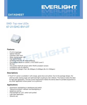
1. Product Overview
The 67-21 series is a family of SMD (Surface Mount Device) top view LEDs designed for indicator and backlighting applications. This specific variant, identified as 67-21/GHC-BV1/2T, emits a brilliant green color. The device is housed in a P-LCC-2 (Plastic Leaded Chip Carrier) package, which features a colorless clear resin encapsulation. A key design feature is the integrated inter-reflector within the package, which optimizes light coupling and results in a wide 120-degree viewing angle. This characteristic makes the LED particularly suitable for use with light pipes, where efficient light transmission is critical. The device is engineered for low current operation, making it an ideal choice for power-sensitive applications such as portable electronic equipment.
1.1 Core Features and Advantages
- Afifi: Standard P-LCC-2 surface mount package.
- Optics: Designed as an optical indicator with colorless clear resin for pure color output.
- Viewing Angle: Exceptionally wide 120-degree viewing angle.
- Performance: High-performance light output.
- Assembly: Compatible with IR reflow soldering processes.
- Reliability: Preconditioning is based on JEDEC J-STD-020D Level 3 standards for moisture sensitivity.
- Compliance: The product is Pb-free (lead-free), compliant with the EU RoHS directive, EU REACH regulations, and is Halogen Free (Br<900ppm, Cl<900ppm, Br+Cl<1500ppm).
1.2 Target Applications
The 67-21 series LEDs are versatile components suitable for a broad range of applications:
- Automotive: Backlighting for dashboard instruments and switches.
- Telecommunications: Status indicators and backlighting in telephones and fax machines.
- Display Technology: Flat backlighting for LCD panels, switches, and symbols.
- Light Guidance: Ideal for light pipe applications due to the wide viewing angle and optimized light coupling.
- General Use: Any application requiring a reliable, bright indicator LED.
2. Technical Parameter Analysis
This section provides a detailed, objective interpretation of the key electrical, optical, and thermal parameters defined in the datasheet. Understanding these limits and characteristics is essential for reliable circuit design.
2.1 Absolute Maximum Ratings
These ratings define the stress limits beyond which permanent damage to the device may occur. Operation at or near these limits is not recommended for extended periods.
- Reverse Voltage (VR): 5 V. Exceeding this voltage in reverse bias can cause junction breakdown.
- Continuous Forward Current (IF): 25 mA. The maximum DC current that can be applied continuously.
- Peak Forward Current (IFP): 100 mA (at 1/10 duty cycle, 1 kHz). Suitable for short pulse operation but not for DC.
- Power Dissipation (Pd): 110 mW. The maximum power the package can dissipate, calculated as VF * IF.
- Operating Temperature (Topr): -40 to +85 °C. The ambient temperature range for normal operation.
- Storage Temperature (Tstg): -40 to +90 °C.
- ESD (HBM): 150 V. This is a relatively low ESD rating, indicating the device is sensitive to electrostatic discharge. Proper ESD handling procedures are mandatory.
- Soldering Temperature: Reflow: 260°C peak for 10 seconds max. Hand soldering: 350°C for 3 seconds max per terminal.
2.2 Electro-Optical Characteristics
These are the typical performance parameters measured at a forward current (IF) of 20 mA and an ambient temperature (Ta) of 25°C. They define the light output and electrical behavior under normal operating conditions.
- Luminous Intensity (Iv): 715 mcd (Min), 1120 mcd (Max). This is the measure of perceived brightness to the human eye. The wide range indicates the device is binned (see Section 3).
- Viewing Angle (2θ1/2): 120 degrees (Typical). The angle at which the luminous intensity is half of the peak intensity. Confirms the wide viewing angle claim.
- Peak Wavelength (λp): 518 nm (Typical). The wavelength at which the spectral power distribution is maximum.
- Dominant Wavelength (λd): 523.5 nm (Min), 533.5 nm (Max). This wavelength corresponds to the perceived color (green) and is also binned.
- Spectral Bandwidth (Δλ): 35 nm (Typical). The width of the emitted spectrum at half the maximum power (FWHM).
- Forward Voltage (VF): 2.7 V (Min), 4.3 V (Max) at 20mA. The voltage drop across the LED when conducting. This range necessitates current-limiting circuitry.
- Reverse Current (IR): 50 µA (Max) at VR=5V. The small leakage current when the device is reverse-biased.
Parameter Tolerances: The datasheet specifies additional tolerances: Luminous Intensity (±11%), Dominant Wavelength (±1nm), and Forward Voltage (±0.1V). These must be factored into worst-case design scenarios.
3. Binning System Explanation
To ensure consistent color and brightness in production, LEDs are sorted into bins based on key parameters. The 67-21 series uses a two-dimensional binning system.
3.1 Binning na Tsawon Tsinkaya (Launi)
LEDs are grouped by their dominant wavelength, which directly affects the perceived hue of the green light. The bins are labeled B13 through B17.
- B13: 523.5 nm to 525.5 nm
- B14: 525.5 nm to 527.5 nm
- B15: 527.5 nm to 529.5 nm
- B16: 529.5 nm to 531.5 nm
- B17: 531.5 nm to 533.5 nm
This allows designers to select LEDs with a very specific shade of green for applications where color consistency is critical.
3.2 Binning na Ƙarfin Haskakawa (Haske)
LEDs are also sorted based on their light output at 20mA. The bins are labeled V1 and V2.
- V1: 715 mcd to 900 mcd
- V2: 900 mcd to 1120 mcd
Selecting a higher bin (V2) ensures brighter indicators. For applications requiring uniform panel brightness, LEDs from the same intensity bin should be used.
4. Mechanical and Package Information
4.1 Package Dimensions
The LED is housed in a standard P-LCC-2 package. The detailed dimensional drawing provides critical measurements for PCB (Printed Circuit Board) land pattern design, including body size, lead spacing, and overall height. Adherence to these dimensions is necessary for proper placement and soldering. The typical tolerance for unspecified dimensions is ±0.1 mm.
4.2 Polarity Identification
A matsayin na'urar mai tashoshi biyu, daidaitaccen tabbataccen ƙarfi yana da mahimmanci. Zanen saman bayanan bayanai yana nuna mai gano cathode (yawanci tsaga, kore ɗigo, ko wasu alama akan kunshin). Haɗa LED a cikin karkatar da baya zai hana shi haskakawa kuma, idan ƙarfin baya ya wuce 5V, yana iya lalata na'urar.
5. Soldering and Assembly Guidelines
Proper handling and soldering are crucial for reliability, especially given the device's moisture sensitivity level (MSL 3).
5.1 Storage and Handling
- Components are shipped in moisture-resistant bags with desiccant.
- The bag must only be opened immediately before use.
- The recommended environment after opening is <30°C and <60% Relative Humidity.
- If the moisture sensitivity indicator card shows excessive moisture, the components must be baked at 60°C ±5°C for 24 hours before use.
- The device is sensitive to ESD (150V HBM). Use appropriate ESD-safe workstations and handling procedures.
5.2 Reflow Soldering Profile
The datasheet provides a detailed Pb-free reflow soldering temperature profile:
- Pre-heating: 150-200°C for 60-120 seconds (ramp rate ≤3°C/sec).
- Time Above Liquidus (217°C): 60-150 seconds.
- Peak Temperature: 260°C maximum, held for a maximum of 10 seconds.
- Ramp-down: Cooling rate should not exceed 6°C/sec above 255°C.
Critical Notes:
- Reflow soldering should not be performed more than two times.
- Avoid mechanical stress on the LED during heating and cooling.
- Do not warp the PCB after soldering.
5.3 Hand Soldering
If hand soldering is necessary:
- Use a soldering iron with a tip temperature <350°C.
- Limit contact time to ≤3 seconds per terminal.
- Yi amfani da ƙarfe mai ƙarfin wutar lantarki ≤25W.
- A ba da mafi ƙarancin tazarar daƙiƙa 2 tsakanin yin solder kowane tashoshi don hana zafi sosai.
- Yin solder da hannu yana ɗaukar haɗarin lalacewa ta zafi mafi girma.
5.4 Rework and Repair
Repair after the LED is soldered is strongly discouraged. If unavoidable:
- A dual-head soldering iron must be used to heat both terminals simultaneously, preventing stress on the solder joints.
- The potential for damaging the LED's characteristics during rework must be evaluated beforehand.
6. Packaging and Ordering Information
6.1 Tape and Reel Specifications
The components are supplied on embossed carrier tape wound onto reels for automated pick-and-place assembly.
- Packing Quantity: 2000 pieces per reel.
- Detailed dimensions for the carrier tape pockets, reel hub, and overall reel are provided to ensure compatibility with assembly equipment.
6.2 Label Explanation
The reel label contains key information for traceability and verification:
- CPN: Customer's Product Number
- P/N: Manufacturer's Product Number (e.g., 67-21/GHC-BV1/2T)
- QTY: Packing Quantity
- CAT: Luminous Intensity Rank (e.g., V1, V2)
- HUE: Dominant Wavelength Rank (e.g., B15)
- REF: Forward Voltage Rank
- LOT No: Manufacturing Lot Number for traceability.
7. Application Design Considerations
7.1 Circuit Design
Current Limiting is Mandatory: The forward voltage (VF) has a wide range (2.7V-4.3V). A small change in supply voltage can cause a large, potentially destructive change in current if only a simple series resistor is used. For stable operation and longevity, a constant current driver or a carefully calculated current-limiting resistor is essential. The resistor value (R) can be approximated using Ohm's Law: R = (Vsupply - VF) / IF. Always use the maximum VF from the datasheet for a worst-case design to ensure the current does not exceed 25mA.
7.2 Thermal Management
Duk da karfin wutar lantarki ya yi ƙasa (110mW mafi girma), kiyaye zafin haɗin gwiwa a cikin iyakoki yana da mahimmanci don dogon lokacin aminci da kwanciyar hankali na fitar da haske. Tabbatar da isasshen yanki na tagulla na PCB ko hanyoyin zafi, musamman idan ana aiki a yanayin zafi mai girma ko kusa da matsakaicin halin yanzu.
7.3 Optical Design for Light Pipes
The 120-degree viewing angle and integrated inter-reflector make this LED an excellent source for light pipes. For optimal efficiency:
- Position the LED as close as possible to the light pipe input surface.
- Align the LED centrally under the light pipe.
- Consider using a reflective surface or cavity around the LED to capture and redirect side-emitted light into the pipe.
8. Technical Comparison and Differentiation
The 67-21 series differentiates itself in the market of SMD indicator LEDs through several key attributes:
- Wide Viewing Angle vs. Standard LEDs: Many standard SMD LEDs have viewing angles around 60-80 degrees. The 120-degree angle of the 67-21 series provides much broader visibility, which is a distinct advantage for panel indicators and light pipe applications.
- Optimized for Light Pipes: The specific mention of an "inter reflector" for optimized light coupling is a design feature targeted at a common application challenge, setting it apart from generic LEDs.
- Comprehensive Compliance: Meeting RoHS, REACH, and Halogen-Free standards makes this device suitable for a wide range of global markets and environmentally conscious designs.
- Detailed Binning: The two-parameter (wavelength and intensity) binning provides designers with a high level of control over color consistency and brightness uniformity in their products.
9. Frequently Asked Questions (Based on Technical Parameters)
Q1: Why is a current-limiting resistor absolutely necessary?
A1: LEDs are current-driven devices. Their V-I curve is exponential. Without a resistor, a small increase in supply voltage above the LED's VF causes a very large, uncontrolled increase in current, quickly exceeding the 25mA absolute maximum rating and leading to thermal runaway and failure.
Q2: Ina iya kunna wannan LED da wutar lantarki na 3.3V?
A2: I, amma ana buƙatar ƙirar da aka yi a hankali. Yin amfani da V na yau da kullunF na ~3.5V (tsakanin mafi ƙanƙanta da mafi girma), wutar lantarki na 3.3V ƙila ba za ta isa ba don tura LED daidai, musamman ga raka'o'in da ke da VF a ƙarshen mafi girma na kewayon (4.3V). Ana ba da shawarar yin amfani da ƙarfin wutar lantarki aƙalla 0.5-1.0V sama da mafi girman V da ake tsammaniF To ensure stable current regulation by the series resistor.
Q3: What does "MSL Level 3" mean for my production process?
A3: Moisture Sensitivity Level 3 means the packaged device can be exposed to factory floor conditions (<30°C/60% RH) for up to 168 hours (7 days) after the sealed bag is opened before it requires baking. If not soldered within this timeframe, the absorbed moisture can vaporize during reflow soldering, causing internal delamination or "popcorning," which destroys the component.
Q4: How do I select the right bin (CAT and HUE) for my application?
A4: Don aikace-aikace inda LED-ori da yawa ake gani tare (misali, mashaya haske na matsayi), zaɓi HUE ɗaya (tsawon raƙuman haske) don tabbatar da launi iri ɗaya. Don aikace-aikace masu buƙatar matakan haske na musamman, zaɓi kwandon CAT (ƙarfi) da ya dace. Don aikace-aikace masu mahimmanci, tuntuɓi mai kayan don ƙayyadad da ainihin kwando-ri da ake buƙata.
10. Operational Principles and Technology Trends
10.1 Basic Operating Principle
Wannan LED diode ne na semiconductor wanda ya dogara da kayan InGaN (Indium Gallium Nitride) chip. Lokacin da aka yi amfani da ƙarfin lantarki na gaba wanda ya wuce kofa, electrons da ramuka suna sake haɗuwa a cikin yanki mai aiki na semiconductor, suna sakin makamashi a cikin nau'in photons (haske). Takamaiman abun da ke cikin gawa na InGaN yana ƙayyade makamashin bandgap, wanda kuma ya ayyana madaidaicin tsayin raƙuman haske da aka fitar—a wannan yanayin, a cikin bakan kore (~518-533 nm). Resin mai tsabta mara launi yana kare guntu kuma yana aiki azaman ruwan tabarau, yana siffanta fitowar haske don cimma faɗin kusurwar kallo na digiri 120.
10.2 Industry Trends
The development of SMD indicator LEDs like the 67-21 series follows several key industry trends:
- Miniaturization and Standardization: The use of standard packages like P-LCC-2 allows for automated assembly and reduces board space.
- Increased Efficiency: Ongoing improvements in semiconductor epitaxy and chip design lead to higher luminous intensity (mcd) for the same input current, enabling brighter indicators or lower power consumption.
- Enhanced Reliability and Compliance: There is a strong drive towards Pb-free soldering, halogen-free materials, and compliance with global environmental regulations (RoHS, REACH), as evidenced in this datasheet.
- Application-Specific Optimization: Rather than being generic components, LEDs are increasingly designed with specific applications in mind, such as the inter-reflector in this device for light pipe efficiency.
Disclaimer and Application Restrictions: This product is intended for general indicator and backlighting applications. It is not designed or qualified for high-reliability applications where failure could lead to personal injury or significant property damage, such as military/aerospace systems, automotive safety systems (e.g., brake lights, airbag indicators), or life-critical medical equipment. For such applications, components with appropriate qualifications and reliability data must be selected. The specifications and typical curves provided are for reference; performance is guaranteed only within the stated absolute maximum ratings and operating conditions.
LED Specification Terminology
Complete explanation of LED technical terms
Photoelectric Performance
| Term | Unit/Representation | Simple Explanation | Why Important |
|---|---|---|---|
| Luminous Efficacy | lm/W (lumens per watt) | Light output per watt of electricity, higher means more energy efficient. | Directly determines energy efficiency grade and electricity cost. |
| Luminous Flux | lm (lumens) | Total light emitted by source, commonly called "brightness". | Determines if the light is bright enough. |
| Viewing Angle | ° (degrees), e.g., 120° | Angle where light intensity drops to half, determines beam width. | Affects illumination range and uniformity. |
| CCT (Color Temperature) | K (Kelvin), e.g., 2700K/6500K | Warmth/coolness of light, lower values yellowish/warm, higher whitish/cool. | Determines lighting atmosphere and suitable scenarios. |
| CRI / Ra | Unitless, 0–100 | Ability to render object colors accurately, Ra≥80 is good. | Affects color authenticity, used in high-demand places like malls, museums. |
| SDCM | MacAdam ellipse steps, e.g., "5-step" | Metric ya Consistency ya Rangi, hatua ndogo zina maana rangi inayolingana zaidi. | Inahakikisha rangi sawa kwenye kundi moja la LEDs. |
| Dominant Wavelength | nm (nanometers), e.g., 620nm (red) | Wavelength corresponding to color of colored LEDs. | Determines hue of red, yellow, green monochrome LEDs. |
| Spectral Distribution | Wavelength vs intensity curve | Shows intensity distribution across wavelengths. | Affects color rendering and quality. |
Electrical Parameters
| Term | Symbol | Simple Explanation | Design Considerations |
|---|---|---|---|
| Forward Voltage | Vf | Minimum voltage to turn on LED, like "starting threshold". | Driver voltage must be ≥Vf, voltages add up for series LEDs. |
| Forward Current | If | Current value for normal LED operation. | Usually constant current drive, current determines brightness & lifespan. |
| Max Pulse Current | Ifp | Peak current tolerable for short periods, used for dimming or flashing. | Pulse width & duty cycle must be strictly controlled to avoid damage. |
| Reverse Voltage | Vr | Max reverse voltage LED can withstand, beyond may cause breakdown. | Circuit must prevent reverse connection or voltage spikes. |
| Thermal Resistance | Rth (°C/W) | Resistance to heat transfer from chip to solder, lower is better. | High thermal resistance requires stronger heat dissipation. |
| ESD Immunity | V (HBM), e.g., 1000V | Ability to withstand electrostatic discharge, higher means less vulnerable. | Anti-static measures needed in production, especially for sensitive LEDs. |
Thermal Management & Reliability
| Term | Key Metric | Simple Explanation | Impact |
|---|---|---|---|
| Junction Temperature | Tj (°C) | Actual operating temperature inside LED chip. | Every 10°C reduction may double lifespan; too high causes light decay, color shift. |
| Lumen Depreciation | L70 / L80 (hours) | Time for brightness to drop to 70% or 80% of initial. | Directly defines LED "service life". |
| Lumen Maintenance | % (e.g., 70%) | Percentage of brightness retained after time. | Indicates brightness retention over long-term use. |
| Color Shift | Δu′v′ or MacAdam ellipse | Degree of color change during use. | Affects color consistency in lighting scenes. |
| Thermal Aging | Material degradation | Deterioration due to long-term high temperature. | May cause brightness drop, color change, or open-circuit failure. |
Packaging & Materials
| Term | Common Types | Simple Explanation | Features & Applications |
|---|---|---|---|
| Package Type | EMC, PPA, Ceramic | Housing material protecting chip, providing optical/thermal interface. | EMC: good heat resistance, low cost; Ceramic: better heat dissipation, longer life. |
| Chip Structure | Front, Flip Chip | Chip electrode arrangement. | Flip chip: kona mafuta bora, ufanisi wa juu, kwa nguvu kubwa. |
| Phosphor Coating | YAG, Silicate, Nitride | Covers blue chip, converts some to yellow/red, mixes to white. | Different phosphors affect efficacy, CCT, and CRI. |
| Lens/Optics | Flat, Microlens, TIR | Optical structure on surface controlling light distribution. | Determines viewing angle and light distribution curve. |
Quality Control & Binning
| Term | Binning Content | Simple Explanation | Purpose |
|---|---|---|---|
| Luminous Flux Bin | Code e.g., 2G, 2H | Grouped by brightness, each group has min/max lumen values. | E kia mau tonu te tūrama i roto i te pātaka kotahi. |
| Voltage Bin | Code e.g., 6W, 6X | Grouped by forward voltage range. | Facilitates driver matching, improves system efficiency. |
| Color Bin | 5-step MacAdam ellipse | Grouped by color coordinates, ensuring tight range. | Guarantees color consistency, avoids uneven color within fixture. |
| CCT Bin | 2700K, 3000K etc. | Grouped by CCT, each has corresponding coordinate range. | Meets different scene CCT requirements. |
Testing & Certification
| Term | Standard/Test | Simple Explanation | Significance |
|---|---|---|---|
| LM-80 | Lumen maintenance test | Long-term lighting at constant temperature, recording brightness decay. | Used to estimate LED life (with TM-21). |
| TM-21 | Life estimation standard | Estimates life under actual conditions based on LM-80 data. | Provides scientific life prediction. |
| IESNA | Illuminating Engineering Society | Covers optical, electrical, thermal test methods. | Industry-recognized test basis. |
| RoHS / REACH | Environmental certification | Ensures no harmful substances (lead, mercury). | Market access requirement internationally. |
| ENERGY STAR / DLC | Ilimin ingancin makamashi | Ilimin ingancin makamashi da aiki don hasken wuta. | Used in government procurement, subsidy programs, enhances competitiveness. |