Table of Contents
- 1. Product Overview
- 1.1 Core Advantages and Target Market
- 2. In-depth Analysis of Technical Parameters
- 2.1 Absolute Maximum Ratings
- 2.2 Electrical Characteristics
- 2.3 Transmission Characteristics
- 2.4 Switching Characteristics
- 3. Mechanical and Package Information
- 4. Soldering and Assembly Guide
- 5. Packaging and Ordering Information
- 6. Application Suggestions
- 6.1 Typical Application Scenarios
- 6.2 Design Considerations
- 7. Technical Comparison and Differentiation
- 8. Frequently Asked Questions (Based on Technical Parameters)
- 9. Practical Design Cases
- 10. Working Principles
- 11. Industry Trends and Background
1. Product Overview
6N138 and 6N139 are high-performance, low-input-current optocouplers featuring a split Darlington phototransistor output stage. These devices are designed to provide an extremely high Current Transfer Ratio (CTR), enabling reliable signal transmission with minimal input drive current. They are housed in a standard 8-pin Dual In-line Package (DIP) and are available with options for wide pin spacing and surface-mount configurations. Their primary function is to provide electrical isolation between input and output circuits, protecting sensitive logic circuits from voltage spikes and ground loops.
1.1 Core Advantages and Target Market
The key advantage of these optocouplers lies in their typical CTR of up to 2000%, which allows them to interface directly with low-current logic signals without requiring additional amplification. They are certified by major international safety agencies (UL, cUL, VDE, SEMKO, NEMKO, DEMKO, FIMKO) and offer a high isolation voltage of 5000 Vrms. These characteristics make them ideal for industrial, telecommunications, and computing applications that demand high noise immunity, safety isolation, and signal integrity. Target markets include industrial automation, power supply feedback loops, digital interface isolation, and communication line receivers.
2. In-depth Analysis of Technical Parameters
This section provides an objective interpretation of the key electrical and optical parameters specified in the datasheet.
2.1 Absolute Maximum Ratings
这些额定值定义了可能导致永久损坏的应力极限。输入红外LED的最大连续正向电流(IF)为20 mA,并能承受1 A的峰值瞬态电流(持续时间极短,<1 µs)。输出晶体管的最大集电极电流(IO)为60 mA,其功耗(PO)限制在100 mW。器件可在-40°C至+85°C的环境温度范围内工作。5000 Vrms的隔离电压是关键的安全参数,测试时所有输入引脚短路在一起,所有输出引脚短路在一起。
2.2 Electrical Characteristics
Electrical characteristics are guaranteed over the commercial temperature range of 0°C to 70°C. For the input LED, the typical forward voltage (VF) is 1.3V at IF = 1.6 mA. The output section parameters of the 6N138 and 6N139 differ slightly. Under the same conditions (IF=0mA, VCC=18V), the 6N139 typically provides a lower logic high-level output current (IOH) leakage of 0.01 µA, compared to 100 µA for the 6N138. When the LED is driven at 1.6 mA, the typical supply current (ICCL) for both in the logic low state is 0.6 mA.
2.3 Transmission Characteristics
Current Transfer Ratio (CTR) is the most critical parameter, defined as (IC / IF) * 100%. The minimum CTR for 6N139 is 400% at IF=0.5mA and 500% at IF=1.6mA. The minimum CTR for 6N138 is 300% at IF=1.6mA. The typical value for both is 2000-2500%, indicating high sensitivity. The logic low-level output voltage (VOL) is specified under various load conditions, with a maximum of 0.4V, ensuring compatibility with standard TTL and CMOS logic levels.
2.4 Switching Characteristics
Switching speed depends on input drive current and load resistance. Propagation delay times (tPLH, tPHL) are given for specific test conditions. For example, under IF=0.5mA and RL=4.7kΩ, the typical tPHL for 6N139 is 5 µs and tPLH is 16 µs. Increasing IF to 12mA and RL=270Ω improves the speed significantly to 0.2 µs and 1.7 µs, respectively. The 6N138 is generally slower under its specified test conditions (IF=1.6mA, RL=2.2kΩ). The common-mode transient immunity (CMTI) for both is specified as a minimum of 1000 V/µs for both logic high and low levels, indicating good noise rejection capability against fast voltage transients across the isolation barrier.
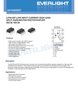
3. Mechanical and Package Information
The device uses a standard 8-pin DIP package. The pin configuration is as follows: Pin 1: No Connection, Pin 2: Anode, Pin 3: Cathode, Pin 4: No Connection, Pin 5: Ground (Gnd), Pin 6: Output (Vout), Pin 7: Base (VB), Pin 8: Supply Voltage (VCC). The base pin (7) provides access to the phototransistor base, which can be used to connect a speed-up resistor or capacitor for trade-offs between bandwidth and stability. Package options include standard DIP, wide lead bend (0.4-inch spacing), and surface-mount lead forms (S-type and thin S1-type).
4. Soldering and Assembly Guide
The absolute maximum rating for soldering temperature is 260°C for 10 seconds. This applies to wave soldering or reflow processes. Standard precautions for handling ESD-sensitive devices should be observed. The device should be stored within the specified storage temperature range of -55°C to +125°C.
5. Packaging and Ordering Information
The part number format is: 6N13XY(Z)-V. 'X' is the part number (8 for 6N138, 9 for 6N139). 'Y' indicates the lead form option: blank for standard DIP (45/tube), 'M' for wide lead bend (45/tube), 'S' for surface mount, 'S1' for low-profile surface mount. 'Z' specifies the tape and reel packaging option for SMD parts: 'TA' or 'TB' (1000/reel). 'V' is an optional suffix for VDE certification. Users must select the correct combination based on assembly requirements.
6. Application Suggestions
6.1 Typical Application Scenarios
The datasheet lists several key applications: digital logic ground isolation, RS-232C line receivers, low input current line receivers, microprocessor bus isolation, and current loop receivers. Their high CTR makes them very suitable for interfacing directly with microcontroller GPIO pins, isolating sensor signals in noisy environments, or providing electrical isolation in serial communication lines such as RS-232 or RS-485.
6.2 Design Considerations
1. Input Current Limiting:An external series resistor must be used to limit the LED forward current (IF) within the absolute maximum rating and the desired operating range. The required resistor value is (Vdrive - VF) / IF.Output Load:The output transistor acts as a current sink. The load resistor (connected between VCC and pin 6) should be chosen to set the desired output voltage swing and switching speed. A smaller resistor increases speed but also increases power dissipation.Speed vs. Stability Trade-off:Connecting a resistor (typically 10kΩ to 1MΩ) from the base pin (7) to ground can improve stability and noise immunity, but it will reduce CTR and slow down the switching speed. A capacitor can be connected in parallel for further filtering.Power Supply Decoupling:It is good practice to place a 0.1 µF ceramic capacitor from the VCC pin (8) to ground nearby to suppress noise.
7. Technical Comparison and Differentiation
The primary differentiation of the 6N138/6N139 series lies in their split Darlington configuration and extremely high CTR. Compared to standard single-transistor optocouplers (e.g., the 4N25 series), these devices offer significantly higher sensitivity, enabling them to be driven directly by low-current CMOS logic. Compared to newer digital isolators, they provide a simpler, analog solution, offering excellent cost-effectiveness for applications requiring basic isolation without the need for ultra-high speed or complex protocols. The accessibility of the base pin provides designers with unique freedom to customize frequency response and noise immunity.
8. Frequently Asked Questions (Based on Technical Parameters)
Q1: What is the main difference between 6N138 and 6N139?
A1: The main difference lies in their electrical specifications. The 6N139 typically offers better performance: a higher minimum CTR (500% vs. 300% at IF=1.6mA), lower output leakage current in the off state, and slightly different switching characteristics under test conditions. The 6N138 is a lower-specification model.
Q2: How to select the value of the input current limiting resistor?
A2: Ayyana ƙarfin kwarara mai zuwa (IF) da ake buƙata bisa aikace-aikacenku (misali, 1.6 mA yana iya samun daidaito mai kyau tsakanin sauri da CTR). Auna ko yi amfani da VF na yau da kullun daga takardar bayanan (1.3V). Idan ƙarfin fitarwa na ku shine 5V, to resistor R = (5V - 1.3V) / 0.0016A = 2312.5Ω. Resistor na yau da kullun 2.2kΩ zai zama zaɓi mai dacewa.
Q3: Me ya sa saurin sauya mai haɗa haske na ya yi jinkiri?
A3: Saurin sauya yana shafar IF da resistor na kaya RL sosai. Don haɓaka sauri, kuna iya: a) ƙara ƙarfin kwarara mai fitar da LED (IF). b) Rage ƙimar resistor na kaya (RL) akan mai tattara fitarwa. c) Zaɓi, yi amfani da ƙafar tushe (7) ta hanyar ƙaramin resistor zuwa ƙasa don sakin cajin ajiya, amma wannan zai rage CTR.
Q4: What does "Common-Mode Transient Immunity" mean?
A4: It measures a device's ability to ignore fast voltage spikes that appear simultaneously on both sides of an isolation barrier. A high CMTI (e.g., 1000 V/µs) means the output will not falsely trigger due to such noise, which is crucial in noisy power environments.
9. Practical Design Cases
Case: Isolating microcontroller UART signals for RS-232 communication.
The microcontroller's 3.3V UART TX line requires isolation before connecting to an RS-232 transceiver chip on a different ground plane. A 6N139 can be used. The microcontroller pin drives an LED via a 1kΩ resistor (IF ~ (3.3V-1.3V)/1k = 2mA). The output collector (pin 6) is connected to the input pin of the RS-232 chip via a 4.7kΩ pull-up resistor to the RS-232 chip's VCC (5V). The base pin (7) is left floating or connected to ground through a large resistor (e.g., 1MΩ) for improved stability. This simple circuit provides robust isolation, protecting the microcontroller from ground potential shifts or surges on the RS-232 line while maintaining signal integrity.
10. Working Principles
The device operates based on the principle of optoelectronic coupling. Current applied to the input pins (anode and cathode) causes an infrared light-emitting diode (LED) to emit light. This light passes through a transparent isolation gap and strikes the photosensitive base region of a shunt Darlington silicon phototransistor. The incident light generates a base current, which is amplified by the two transistor stages, resulting in a larger collector current at the output. The "shunt" configuration typically means the base of the first transistor is accessible (pin 7), allowing for external biasing. Complete electrical isolation between the input LED and the output transistor is provided by the molded plastic package with high dielectric strength.
11. Industry Trends and Background
Optocouplers like the 6N138/139 represent a mature and reliable isolation technology. Current trends in signal isolation include the growth of digital isolators based on CMOS as well as RF or capacitive coupling, which offer superior speed, power efficiency, and integration (multiple channels in a single package). However, optocouplers maintain strong advantages in certain areas: they provide very high working voltage isolation (thousands of volts), excellent common-mode transient immunity, simplicity, and robustness against high dv/dt stress. They are often preferred in high-noise industrial environments, power supply feedback loops, and applications where proven reliability and safety certifications are critical. The development of new LED and detector materials continues to improve optocoupler speed and CTR, ensuring their coexistence with new technologies and maintaining their relevance.
Detailed Explanation of LED Specification Terminology
Complete Explanation of LED Technical Terminology
I. Core Indicators of Photoelectric Performance
| Terminology | Unit/Representation | Popular Explanation | Why It Is Important |
|---|---|---|---|
| Luminous Efficacy | lm/W | The luminous flux emitted per watt of electrical power; higher values indicate greater energy efficiency. | Directly determines the energy efficiency rating and electricity cost of the luminaire. |
| Luminous Flux | lm (lumen) | The total amount of light emitted by a light source, commonly known as "brightness". | Determines whether a luminaire is bright enough. |
| Viewing Angle | ° (degrees), e.g., 120° | The angle at which light intensity drops to half, determining the beam width. | Affects the illumination range and uniformity. |
| Correlated Color Temperature (CCT) | K (Kelvin), e.g., 2700K/6500K | The warmth or coolness of light color; lower values are yellowish/warm, higher values are whitish/cool. | Determines the lighting atmosphere and suitable application scenarios. |
| Color Rendering Index (CRI / Ra) | Unitless, 0–100 | The ability of a light source to restore the true color of an object, Ra≥80 is recommended. | Affects color authenticity, used in high-demand places such as shopping malls and art galleries. |
| SDCM (Standard Deviation of Color Matching) | MacAdam ellipse steps, e.g., "5-step" | A quantitative indicator of color consistency; a smaller step number indicates higher color consistency. | Ensure no color difference among the same batch of luminaires. |
| Dominant Wavelength | nm (nanometer), misali 620nm (ja) | Rangi ya LED zenye rangi zinazolingana na thamani ya urefu wa wimbi. | Kuamua rangi ya LED moja kama nyekundu, manjano, kijani, n.k. |
| Spectral Distribution | Wavelength vs. Intensity Curve | Display the intensity distribution of light emitted by the LED across various wavelengths. | Affects color rendering and color quality. |
II. Electrical Parameters
| Terminology | Symbol | Popular Explanation | Design Considerations |
|---|---|---|---|
| Forward Voltage | Vf | The minimum voltage required to light up an LED, similar to a "starting threshold". | The driving power supply voltage must be ≥ Vf; voltages add up when multiple LEDs are connected in series. |
| Forward Current | If | The current value that makes the LED emit light normally. | Constant current drive is often used, as the current determines brightness and lifespan. |
| Maximum Pulse Current | Ifp | Peak current that can be sustained for a short period, used for dimming or flashing. | Pulse width and duty cycle must be strictly controlled to prevent overheating damage. |
| Reverse Voltage | Vr | The maximum reverse voltage that an LED can withstand; exceeding it may cause breakdown. | The circuit must be protected against reverse polarity or voltage surges. |
| Thermal Resistance | Rth (°C/W) | The resistance to heat transfer from the chip to the solder joint. A lower value indicates better heat dissipation. | High thermal resistance requires a stronger heat dissipation design; otherwise, the junction temperature will rise. |
| ESD Immunity | V (HBM), e.g., 1000V | The higher the value, the more resistant it is to electrostatic damage. | Anti-static measures must be taken during production, especially for high-sensitivity LEDs. |
III. Thermal Management and Reliability
| Terminology | Key Indicators | Popular Explanation | Impact |
|---|---|---|---|
| Junction Temperature | Tj (°C) | The actual operating temperature inside the LED chip. | For every 10°C reduction, lifespan may double; excessively high temperatures cause lumen depreciation and color shift. |
| Lumen Depreciation | L70 / L80 (hours) | The time required for brightness to drop to 70% or 80% of its initial value. | Directly defines the "service life" of an LED. |
| Lumen Maintenance | % (e.g., 70%) | The percentage of remaining brightness after a period of use. | Characterizes the ability to maintain brightness after long-term use. |
| Color Shift | Δu′v′ or MacAdam ellipse | The degree of color change during use. | Affects the color consistency of the lighting scene. |
| Thermal Aging | Material performance degradation | Deterioration of packaging materials due to prolonged high temperatures. | May lead to decreased brightness, color shift, or open-circuit failure. |
IV. Packaging and Materials
| Terminology | Common Types | Popular Explanation | Characteristics and Applications |
|---|---|---|---|
| Packaging Type | EMC, PPA, Ceramic | The housing material that protects the chip and provides optical and thermal interfaces. | EMC tahan panas baik, biaya rendah; keramik pendinginan unggul, umur panjang. |
| Struktur chip | Face-up, Flip Chip | Chip electrode arrangement method. | Flip Chip offers better heat dissipation and higher luminous efficacy, suitable for high-power applications. |
| Phosphor coating | YAG, silicate, nitride | Covered on the blue light chip, partially converted into yellow/red light, mixed into white light. | Different phosphors affect luminous efficacy, color temperature, and color rendering. |
| Lens/Optical design | Flat, Microlens, Total Internal Reflection | Optical structure on the encapsulation surface, controlling light distribution. | Determine the beam angle and light distribution curve. |
V. Quality Control and Binning
| Terminology | Binning Content | Popular Explanation | Purpose |
|---|---|---|---|
| Luminous Flux Classification | Codes such as 2G, 2H | Group by brightness level, each group has a minimum/maximum lumen value. | Ensure consistent brightness for the same batch of products. |
| Voltage binning | Codes such as 6W, 6X | Group by forward voltage range. | Facilitates driver matching and improves system efficiency. |
| Color binning. | 5-step MacAdam Ellipse | Group by color coordinates to ensure colors fall within a minimal range. | Ensure color consistency to avoid uneven color within the same luminaire. |
| Color temperature binning | 2700K, 3000K, etc. | Grouped by color temperature, each group has a corresponding coordinate range. | Meet the color temperature requirements of different scenarios. |
VI. Testing and Certification
| Terminology | Standard/Test | Popular Explanation | Significance |
|---|---|---|---|
| LM-80 | Lumen Maintenance Test | Record brightness attenuation data under constant temperature conditions over a long period of illumination. | Used to estimate LED lifetime (in conjunction with TM-21). |
| TM-21 | Standard for Life Projection | Projecting lifetime under actual use conditions based on LM-80 data. | Provide scientific life prediction. |
| IESNA Standard | Illuminating Engineering Society Standard | Covers optical, electrical, and thermal testing methods. | Industry-recognized testing basis. |
| RoHS / REACH | Environmental Certification | Ensure products are free from hazardous substances (e.g., lead, mercury). | Market access requirements for entering the international market. |
| ENERGY STAR / DLC | Energy Efficiency Certification | Energy Efficiency and Performance Certification for Lighting Products. | Commonly used in government procurement and subsidy programs to enhance market competitiveness. |