Table of Contents
- 1. Product Overview
- 1.1 Core Specifications and Component Selection
- 2. Technical Parameters: In-depth and Objective Interpretation
- 2.1 Absolute Maximum Ratings
- 2.2 Electro-Optical Characteristics
- 3. Performance Curve Analysis
- 3.1 Power Consumption vs. Ambient Temperature
- 3.2 Spectral Distribution
- 3.3 Relationship Between Peak Emission Wavelength and Ambient Temperature
- 3.4 Relationship between Forward Current and Forward Voltage (I-V Curve)
- 3.5 Relationship between Relative Radiation Intensity and Angular Displacement
- 4. Mechanical and Packaging Information
- 4.1 Package Dimensions
- 4.2 Polarity Identification
- 4.3 Carrier Tape and Reel Specifications
- 5. Welding and Assembly Guide
- 5.1 Reflow Soldering Process
- 5.2 Manual Soldering
- 5.3 Rework and Repair
- 6. Storage and Moisture Sensitivity
- 7. Application Suggestions
- 7.1 Typical Application Scenarios
- 7.2 Key Design Considerations
- 8. Packaging and Ordering Information
- 8.1 Packaging Procedure
- 8.2 Label Specifications
- 9. Frequently Asked Questions (Based on Technical Parameters)
- 10. Working Principle and Technical Background
- 10.1 Basic Working Principle
- 10.2 Role in Optoelectronic Systems
- 10.3 Industry Trends and Background
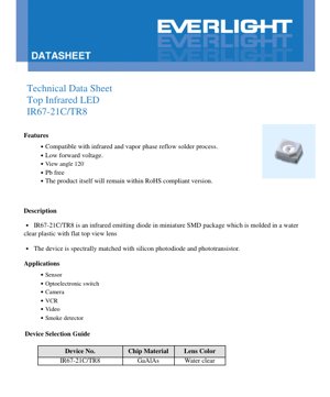
1. Product Overview
IR67-21C/TR8 is a top-view infrared emitting diode housed in a miniature surface mount device (SMD) package. The device features a transparent plastic package with a flat lens on top and is designed to be compatible with modern infrared and vapor phase reflow soldering processes. Its primary function is to emit infrared light with a peak wavelength matched to silicon photodiodes and phototransistors, making it a core component in various sensing and switching applications.
The key advantages of this component include its low forward voltage requirement, wide 120-degree viewing angle, and compliance with lead-free and RoHS environmental standards. Its miniature SMD footprint allows for high-density mounting on printed circuit boards, which is crucial for compact consumer electronics and industrial electronic products.
1.1 Core Specifications and Component Selection
The fundamental specifications defining the IR67-21C/TR8 are its chip material and optical characteristics. The light-emitting chip is constructed from Gallium Aluminum Arsenide (GaAlAs), a semiconductor material exceptionally well-suited for generating infrared radiation. The package employs a transparent lens that does not filter the emitted infrared light, thereby ensuring maximum radiant intensity output. This combination of a GaAlAs chip and a transparent lens is specifically designed for optimal performance in sensor applications where the strength of the detected signal is critical.
2. Technical Parameters: In-depth and Objective Interpretation
This section provides a detailed and objective analysis of the electrical, optical, and thermal parameters specified for the IR67-21C/TR8 infrared LED. Understanding these ratings is crucial for reliable circuit design and ensuring the long-term operational integrity of the device.
2.1 Absolute Maximum Ratings
Absolute Maximum Ratings define the stress limits beyond which permanent damage to the device may occur. These are not recommended operating conditions but thresholds that must not be exceeded under any circumstances, including during transient events.
- Continuous Forward Current (IF)): 65 mA. This is the maximum DC current that can flow through the LED junction indefinitely at an ambient temperature (Ta) of 25°C.
- Peak Forward Current (IFP)): 1.0 A. This high current is only permitted under strict pulse conditions: pulse width ≤ 100 µs and duty cycle ≤ 1%. This rating applies to applications requiring brief, high-intensity infrared light pulses.
- Reverse voltage (VR)): 5 V. Applying a reverse bias voltage exceeding this value may lead to junction breakdown.
- Power consumption (Pd)): 130 mW at 25°C. This is the maximum power that the package can dissipate as heat. As shown in the derating curve, the actual allowable power decreases as the ambient temperature increases.
- Junction-to-ambient thermal resistance (Rthj-a)): 400 K/W. This parameter quantifies the efficiency of heat transfer from the semiconductor junction to the surrounding air. A lower value indicates better heat dissipation. Based on this value, for every watt of power dissipated, the junction temperature will rise by 400°C above the ambient temperature.
- Soldering temperature (Tsol)): Maximum 260°C, duration not exceeding 5 seconds. This defines the tolerance for the reflow soldering temperature profile.
2.2 Electro-Optical Characteristics
These parameters are measured under standard test conditions at 25°C and describe the performance of the device under normal operation. The 'Typical' column represents typical or expected values, while the 'Min' and 'Max' define the guaranteed performance limits.
- Radiant Intensity (Ie)): This is the optical power emitted per unit solid angle (measured in milliwatts per steradian, mW/sr). At a standard drive current of 20mA, the typical radiant intensity is 1.5 mW/sr, with a guaranteed minimum of 1.0 mW/sr. Under pulsed high-current conditions (100mA, ≤100µs, ≤1% duty cycle), the intensity can reach a typical value of 20 mW/sr.
- Peak Wavelength (λp)): 940 nm (typical). This is the wavelength at which the LED emits the most optical power. It spectrally matches the peak sensitivity of common silicon-based photodetectors.
- Spectral Bandwidth (Δλ)): 45 nm (typical value). This defines the wavelength range of emission, typically measured at half of the maximum intensity (Full Width at Half Maximum, FWHM). A 45nm bandwidth centered at 940nm means significant emission from approximately 917.5nm to 962.5nm.
- Forward Voltage (VF)): At 20mA, the typical forward voltage is 1.2V, with a maximum of 1.5V. Under pulsed 100mA conditions, VFincreases to a typical 1.4V (maximum 1.8V). This low VFis advantageous for low-voltage and battery-powered applications.
- Perspective (2θ1/2)): 120 degrees. This is the full angle (measured on-axis) at which the radiant intensity drops to half of its peak value. The wide 120° angle provides broad, diffuse illumination, ideal for proximity or presence sensing where the target position may vary.
3. Performance Curve Analysis
The datasheet contains several characteristic curves that illustrate how key parameters vary with operating conditions. These graphs are crucial for dynamic system design.
3.1 Power Consumption vs. Ambient Temperature
This derating curve shows that the maximum allowable power dissipation (Pd) decreases linearly from 130 mW at 25°C to approximately 0 mW at around 150°C. Designers must use this graph to calculate the safe operating current for their specific maximum ambient temperature. For example, if the maximum ambient temperature is 85°C, the graph shows a significantly reduced allowable power dissipation, which in turn limits the maximum permissible forward current.
3.2 Spectral Distribution
The spectral distribution curve plots relative radiant intensity versus wavelength. It visually confirms the peak wavelength of 940nm and the spectral bandwidth of approximately 45nm. The curve typically exhibits a Gaussian shape, centered around the peak wavelength.
3.3 Relationship Between Peak Emission Wavelength and Ambient Temperature
This curve illustrates the temperature dependence of the peak wavelength. Typically, as the junction temperature increases, the peak wavelength of an LED shifts towards longer wavelengths ("red shift"). This graph quantifies this shift, which is crucial for applications requiring precise spectral matching, as the detector's sensitivity may also be temperature-dependent.
3.4 Relationship between Forward Current and Forward Voltage (I-V Curve)
The I-V curve is nonlinear, similar to a standard diode. It shows the relationship between the current through the LED and the voltage across its terminals. The "knee" of this curve is approximately near the typical forward voltage. This curve is useful for designing current-limiting circuits, especially when driving an LED with a voltage source.
3.5 Relationship between Relative Radiation Intensity and Angular Displacement
This polar plot illustrates the spatial emission pattern. It confirms the 120° viewing angle and shows how the intensity is distributed. The pattern of a flat-top LED in a transparent package is typically close to a Lambertian distribution, where the intensity is proportional to the cosine of the angle from the normal (center).
4. Mechanical and Packaging Information
4.1 Package Dimensions
IR67-21C/TR8 uses a miniature SMD package. The dimension drawing provides all key dimensions required for PCB pad design, including body length, width, height, lead pitch, and pad size. Key dimensions include overall dimensions (e.g., approximately 3.2mm x 2.8mm, but exact values must be taken from the drawing), distances between pads, and the recommended pad pattern to ensure reliable soldering. Unless otherwise specified, all dimensions are in millimeters, with a standard tolerance of ±0.1mm.
4.2 Polarity Identification
The package contains markings or features (such as a notch, bevel, or cathode mark) to identify the anode and cathode terminals. Care must be taken to ensure correct polarity during assembly, as applying reverse bias may damage the device.
4.3 Carrier Tape and Reel Specifications
For automatic assembly, components are supplied in embossed carrier tape, wound onto reels. The datasheet provides carrier tape dimensions, including pocket size, pitch, and tape width. Reels typically contain 2000 components. These dimensions are critical for programming the pick-and-place machine.
5. Welding and Assembly Guide
Proper handling and soldering are crucial to prevent LED damage and ensure long-term reliability.
5.1 Reflow Soldering Process
This device is compatible with infrared and vapor phase reflow processes. A recommended lead-free solder temperature profile is provided, specifying preheating, soaking, reflow peak temperature (must not exceed 260°C), and cooling rate. Reflow soldering should not be performed more than twice. No stress should be applied to the LED body during heating, and the PCB should not warp after soldering.
5.2 Manual Soldering
If manual soldering must be performed, extreme caution is required. The soldering iron tip temperature must be below 350°C, and the contact time for each terminal should not exceed 3 seconds. It is recommended to use a low-power soldering iron (≤25W). A cooling interval of at least 2 seconds should be observed between soldering each terminal. The datasheet strongly advises that manual soldering often leads to damage.
5.3 Rework and Repair
It is not recommended to perform repairs after LED soldering. If unavoidable, use a dual-tip soldering iron to simultaneously heat both terminals to minimize thermal stress. The possibility of damaging LED characteristics during rework must be evaluated beforehand.
6. Storage and Moisture Sensitivity
IR67-21C/TR8 is sensitive to moisture. Precautions must be taken to prevent "popcorn" phenomenon (package cracking due to rapid vapor expansion) during reflow.
- The moisture barrier bag should not be opened until the components are ready for use.
- Store at ≤30°C and ≤90% relative humidity (RH) before opening. Shelf life is one year.
- After opening, store at ≤30°C and ≤70% RH. "Floor life" (time allowed out of the bag) is 168 hours (7 days).
- If the silica gel desiccant changes color (indicating saturation) or exceeds the storage time, it needs to be baked at 60 ±5°C for 24 hours before reflow.
7. Application Suggestions
7.1 Typical Application Scenarios
IR67-21C/TR8 is designed for a wide range of optoelectronic applications where invisible infrared light is used for sensing or signal transmission.
- Sensor: Used as a light source for proximity sensors, object detection, and line-following robots.
- Photoelectric switch: Constitutes one half of a photointerrupter or slot-type switch, where an object interrupts the light beam between an LED and a photodetector.
- Consumer electronics: Used in remote control transmitters for televisions, VCRs, and other audio/video equipment (though typically using higher-power LEDs for longer range).
- Imaging: For infrared illumination in security cameras, especially in low-light or night vision modes.
- Security equipmentCan be used as a component in certain smoke detectors that operate on the principle of optical scattering.
7.2 Key Design Considerations
- Current LimitingExternal current-limiting resistors are absolutely essential. LEDs exhibit a steep I-V characteristic, meaning a small increase in voltage leads to a large increase in current, which can cause immediate burnout if not controlled. The resistor value is calculated using Ohm's Law: R = (VPower Supply- VF) / IF.
- Thermal Management: Although SMD packages dissipate heat through PCB pads, careful attention must be paid to the power derating curve, especially in high ambient temperature environments. Sufficient PCB copper area (thermal pad) helps to reduce the junction temperature.
- Spectral MatchingEnsure that the selected photodetector (photodiode, phototransistor) has peak sensitivity around 940nm to achieve the optimal system signal-to-noise ratio.
- Optical DesignThe 120° field of view provides broad coverage. For longer distances or more directional beams, auxiliary optics (lenses) may be required.
8. Packaging and Ordering Information
8.1 Packaging Procedure
LEDs are packaged in moisture barrier aluminum bags containing desiccant and humidity indicator cards. A label is affixed to the bag containing key information for traceability and proper application.
8.2 Label Specifications
The label includes several fields: Customer Part Number (CPN), Manufacturer Part Number (P/N), Package Quantity (QTY), Lot Number (LOT NO), and optical binning information such as Category (CAT, possibly for radiant intensity) and Hue (HUE, for peak wavelength). A Reference Code (REF) may also be present.
9. Frequently Asked Questions (Based on Technical Parameters)
Q: If the continuous current is only 65mA, what is the purpose of the 1.0A peak forward current rating?
A: The peak current rating allows the LED to be driven with very short, high-power pulses. This is useful in applications such as distance measurement (time-of-flight) or data transmission, which require brief, intense bursts of infrared light to overcome ambient noise or travel longer distances without generating excessive average heat.
Q: If my application's ambient temperature is 50°C, how do I determine the safe operating current?
A: You must use the power dissipation vs. ambient temperature derating curve. Locate the point corresponding to 50°C on the curve to determine the maximum allowable power dissipation (Pd(max)) at that temperature. Then, use the typical forward voltage (VF), calculate the maximum safe current: IF(max)= Pd(max)/ VFAlways include a safety margin.
Q: Can I use this LED for a TV remote control?
A: While it emits at the correct wavelength (940nm is standard for remotes), its radiant intensity at 20mA (typically 1.5 mW/sr) may be lower than dedicated remote control LEDs, which are often driven at higher currents or have different optical designs for longer range. It could work for short-range remotes, but for typical living room distances, components specifically designed for higher output may be more suitable.
Q: Why are the storage and baking procedures so specific?
A: Plastic SMD packages absorb moisture from the air. During the high-temperature reflow soldering process, this absorbed moisture rapidly turns into steam, creating internal pressure that can lead to package delamination or chip cracking (the "popcorn" effect). Controlled storage and baking procedures are industry standards (based on JEDEC MSL ratings) designed to safely remove this moisture prior to soldering.
10. Working Principle and Technical Background
10.1 Basic Working Principle
Infrared light-emitting diodes (IR LEDs) operate based on the principle of electroluminescence in a semiconductor p-n junction. When a forward voltage is applied, electrons from the n-type material and holes from the p-type material are injected into the junction region. When these charge carriers recombine, they release energy. In GaAlAs semiconductors, this energy is primarily released in the form of photons in the infrared spectrum (approximately 940 nm). The specific wavelength is determined by the bandgap energy of the semiconductor material, which is achieved by adjusting the ratio of aluminum to gallium in the crystal.
10.2 Role in Optoelectronic Systems
In a typical sensing system, the IR67-21C/TR8 acts as an active signal source. Its light is either received directly by the detector (for transmission sensing), reflected back from the target (for proximity/reflective sensing), or interrupted by an object (for beam-break sensing). The detector converts the modulated or interrupted infrared light into an electrical signal for processing. The 940nm wavelength is an ideal choice because it is invisible to the human eye, avoids interference from most ambient visible light, aligns with the high-sensitivity region of inexpensive silicon detectors, and is less absorbed by air and common materials compared to longer infrared wavelengths.
10.3 Industry Trends and Background
The development of SMD infrared LEDs like the IR67-21C/TR8 is driven by the miniaturization and automation of electronic product assembly. Trends include smaller package sizes, higher radiant intensity per unit area, improved thermal performance, and tighter binning to ensure consistent performance. Concurrently, research continues on new semiconductor materials (e.g., InGaN on silicon for different IR bands) and integrated solutions that combine LED drivers, sensors, and signal processing in a single module (e.g., proximity sensor modules). With the expansion of the Internet of Things (IoT), automotive sensing (e.g., in-cabin monitoring), and industrial automation, the demand for reliable, low-cost infrared components continues to grow.
Detailed Explanation of LED Specification Terminology
Complete Explanation of LED Technical Terminology
I. Core Indicators of Optoelectronic Performance
| Terminology | Unit/Representation | Popular Explanation | Why It Is Important |
|---|---|---|---|
| Luminous Efficacy | lm/W (lumens per watt) | The luminous flux emitted per watt of electrical power; higher values indicate greater energy efficiency. | Directly determines the energy efficiency rating and electricity cost of the lighting fixture. |
| Luminous Flux | lm (lumen) | Total light output from a light source, commonly known as "brightness". | Determines whether a luminaire is bright enough. |
| Viewing Angle | ° (degrees), e.g., 120° | The angle at which light intensity drops to half determines the beam width. | Affects the illumination range and uniformity. |
| Color Temperature (CCT) | K (Kelvin), e.g., 2700K/6500K | The warmth or coolness of light color; lower values are yellowish/warm, higher values are whitish/cool. | Determining the lighting atmosphere and applicable scenarios. |
| Color Rendering Index (CRI / Ra) | Unitless, 0–100 | The ability of a light source to restore the true color of an object, Ra≥80 is recommended. | Affects color authenticity, used in high-demand places such as shopping malls and art galleries. |
| SDCM (Standard Deviation of Color Matching) | MacAdam ellipse steps, e.g., "5-step" | A quantitative indicator of color consistency; a smaller step number indicates higher color consistency. | Ensure no color difference among the same batch of luminaires. |
| Dominant Wavelength | nm (nanometer), e.g., 620nm (red) | The wavelength values corresponding to the colors of colored LEDs. | Determines the hue of monochromatic LEDs such as red, yellow, and green. |
| Spectral Distribution | Wavelength vs. Intensity Curve | Display the intensity distribution of light emitted by the LED across various wavelengths. | Affect color rendering and color quality. |
II. Electrical Parameters
| Terminology | Symbol | Popular Explanation | Design Considerations |
|---|---|---|---|
| Forward Voltage | Vf | The minimum voltage required to light up an LED, similar to a "starting threshold". | The driving power supply voltage must be ≥ Vf; voltages add up when multiple LEDs are connected in series. |
| Forward Current | If | The current value that makes the LED emit light normally. | Constant current drive is often used, as the current determines brightness and lifespan. |
| Matsakaicin ƙarfin wutar lantarki na bugun jini (Pulse Current) | Ifp | Peak current that can be sustained for a short period, used for dimming or flashing. | Pulse width and duty cycle must be strictly controlled to prevent overheating and damage. |
| Reverse Voltage | Vr | The maximum reverse voltage that an LED can withstand; exceeding it may cause breakdown. | The circuit must be protected against reverse polarity or voltage surges. |
| Thermal Resistance | Rth (°C/W) | The resistance to heat flow from the chip to the solder joint. A lower value indicates better heat dissipation. | High thermal resistance requires a more robust thermal design; otherwise, the junction temperature will increase. |
| ESD Immunity | V (HBM), such as 1000V | The higher the value, the more resistant it is to electrostatic damage. | Anti-static measures must be taken during production, especially for high-sensitivity LEDs. |
III. Thermal Management and Reliability
| Terminology | Key Metrics | Popular Explanation | Impact |
|---|---|---|---|
| Junction Temperature | Tj (°C) | The actual operating temperature inside the LED chip. | For every 10°C reduction, lifespan may double; excessively high temperatures cause lumen depreciation and color shift. |
| Lumen Depreciation | L70 / L80 (hours) | The time required for brightness to drop to 70% or 80% of its initial value. | Directly defines the "service life" of an LED. |
| Lumen Maintenance | % (e.g., 70%) | The percentage of remaining brightness after a period of use. | Characterizes the ability to maintain brightness after long-term use. |
| Color Shift | Δu′v′ or MacAdam ellipse | The degree of color change during use. | Affects the color consistency of the lighting scene. |
| Thermal Aging | Material performance degradation | Deterioration of packaging materials due to prolonged high temperatures. | May lead to decreased brightness, color shift, or open-circuit failure. |
IV. Packaging and Materials
| Terminology | Common Types | Popular Explanation | Characteristics and Applications |
|---|---|---|---|
| Packaging Type | EMC, PPA, Ceramic | The housing material that protects the chip and provides optical and thermal interfaces. | EMC tahan panas baik, biaya rendah; keramik pendinginan unggul, umur panjang. |
| Struktur chip | Face-up, Flip Chip | Chip electrode arrangement method. | Flip Chip offers better heat dissipation and higher luminous efficacy, suitable for high-power applications. |
| Phosphor coating | YAG, silicate, nitride | Covered on the blue light chip, partially converted into yellow/red light, mixed into white light. | Different phosphors affect luminous efficacy, color temperature, and color rendering. |
| Lens/Optical design | Planar, Microlens, Total Internal Reflection | Optical structures on the encapsulation surface control light distribution. | Determine the beam angle and light distribution curve. |
V. Quality Control and Binning
| Terminology | Binning Content | Popular Explanation | Purpose |
|---|---|---|---|
| Luminous Flux Classification | Codes such as 2G, 2H | Group by brightness level, each group has a minimum/maximum lumen value. | Ensure consistent brightness within the same batch of products. |
| Voltage binning | Codes such as 6W, 6X | Group by forward voltage range. | Facilitates driver matching and improves system efficiency. |
| Color binning. | 5-step MacAdam Ellipse | Group by color coordinates to ensure colors fall within a minimal range. | Ensure color consistency to avoid uneven color within the same luminaire. |
| Color temperature binning | 2700K, 3000K, etc. | Grouped by color temperature, each group has a corresponding coordinate range. | To meet the color temperature requirements of different scenarios. |
VI. Testing and Certification
| Terminology | Standards/Testing | Popular Explanation | Significance |
|---|---|---|---|
| LM-80 | Lumen Maintenance Test | Record brightness attenuation data under constant temperature conditions over a long period of illumination. | Used to estimate LED lifetime (combined with TM-21). |
| TM-21 | Standard for Life Projection | Projecting lifetime under actual use conditions based on LM-80 data. | Provide scientific life prediction. |
| IESNA Standard | Illuminating Engineering Society Standard | Covers optical, electrical, and thermal testing methods. | Industry-recognized testing basis. |
| RoHS / REACH | Environmental Certification | Ensure products are free from hazardous substances (e.g., lead, mercury). | Market access requirements for entering the international market. |
| ENERGY STAR / DLC | Energy Efficiency Certification | Energy Efficiency and Performance Certification for Lighting Products. | Commonly used in government procurement and subsidy programs to enhance market competitiveness. |