Table of Contents
- 1. Product Overview
- 1.1 Core Advantages and Target Market
- 2. In-depth Technical Parameter Analysis
- 2.1 Absolute Maximum Ratings
- 2.2 Electrical and Optical Characteristics
- F
- Designers should consult the complete graphical data to optimize the operating point for their specific speed, power consumption, and temperature stability requirements.
- 4. Mechanical and Packaging Information
- Recommended Land Pattern
- Indicates optional marking for VDE certification.
- Daidaitaccen alkibla yana da mahimmanci. Alamar mai nuna pin 1 a kan kewaye dole ta yi daidai da alamar pin 1 a kan kewayen PCB. Shigar da kuskure zai haifar da rashin aikin na'urar, kuma yana iya haifar da lalacewa.
- 5.2 Operation and Storage
- 6. Packaging and Ordering Information
- 6.1 Model and Options
- 6.2 Reel Specifications
- 7. Application Design Considerations
- 7.1 Input Circuit Design
- 3.2 Output Circuit Design
- To maximize high isolation capability, careful PCB layout is crucial. According to safety standards, maintain sufficient creepage distance and electrical clearance between the input and output sides of the circuit. Use a ground plane, but consider splitting the ground plane beneath the optocoupler to minimize capacitive coupling across the isolation barrier. Placing bypass capacitors close to both sides of the device pins helps suppress high-frequency noise.
- The key differentiating feature of the ELQ3H4 is its
- 9. Frequently Asked Questions
- 10. Practical Application Examples
- 11. Working Principles
- 12. Technology Trends
1. Product Overview
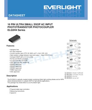
The ELQ3H4 series is a class of optocoupler isolators designed for high-density applications requiring reliable signal isolation. Its core component consists of a gallium arsenide light-emitting diode optically coupled to a silicon NPN phototransistor, all housed within a compact 16-pin ultra-thin small outline package. A key feature of this package is the integrated light shield, which effectively reduces the impact of ambient light on the phototransistor's performance, thereby enhancing signal integrity in noisy electrical environments.
The device is designed to directly accept AC input signals, eliminating the need for external rectification circuits in many applications. Its primary value proposition lies in combining an extremely small form factor with robust isolation performance, while complying with major international safety and environmental standards.RMS。
1.1 Core Advantages and Target Market
The ELQ3H4 optocoupler offers several significant advantages. ItsHalogen-FreeThe structure and compliance with RoHS and lead-free directives make it suitable for environmentally conscious designs. The device is certified by leading safety agencies including UL, VDE, SEMKO, NEMKO, DEMKO, FIMKO, and CQC, facilitating its use in products for global markets with stringent regulatory requirements.
Its primary target application areas are industrial automation and measurement, where noise immunity and safety are critical. These applications include:
- Programmable Logic Controllers:Used to isolate digital I/O signals, communication buses, or analog sensor inputs from the central processing unit.
- Measuring Instrument:Provides isolation in data acquisition systems, multimeters, or oscilloscopes to protect sensitive circuits from high-voltage test points.
- Hybrid Integrated Circuits and Power Supplies:Used as feedback components in isolated switching power supplies, or in custom hybrid modules for gate driving or signal conditioning.
2. In-depth Technical Parameter Analysis
A thorough understanding of electrical and optical parameters is crucial for reliable circuit design. The following section provides a detailed analysis of key specifications.
2.1 Absolute Maximum Ratings
These ratings define the stress limits that may cause permanent damage to the device. Operation under these conditions is not recommended. Key limits for the ELQ3H4 include:
- Input side:Continuous forward current is ±60mA, and the 1μs pulse current is 1A. The power dissipation per channel is 70mW, with a derating factor of 0.7mW/°C.FFFPFP
- Output side:The collector current is 50mA. The collector-emitter voltage is 80V, while the emitter-collector voltage is lower at 7V, indicating the asymmetry in the breakdown characteristics of the phototransistor. The output power dissipation per channel is 150mW, with a derating factor of 1.4mW/°C.CCCEOCEOECOECO
- Isolation and Environment:The device can withstand one minute ofISO3750 VRMSIsolation voltage. Operating temperature range is -55°C to +110°C.
2.2 Electrical and Optical Characteristics
These parameters define the performance of the device under normal operating conditions.AA
Input Characteristics:The forward voltage of a GaAs light-emitting diode at IFFF= 20mA has a typical value of 1.2V and a maximum of 1.4V. The input capacitance is up to 250pF, which can affect high-frequency switching performance.F) is up to 250pF, which can affect high-frequency switching performance.
Output Characteristics:When the light-emitting diode is off, VCEOCEOCEAt =20V, the maximum collector-emitter dark current is 100nA, representing the phototransistor's leakage current. The breakdown voltage confirms its asymmetrical structure.CEOCEOECOECO
Transfer Characteristics:AThis is the core of optocoupler performance.Current Transfer Ratio:
- Defined as under specific conditions (ICCFF/ IF) * 100%. ELQ3H4 in ICEF
- = 1mA, VCEO
- = 5V yana da faɗin kewayon CTR, daga 20% zuwa 300%. Wannan faɗin kewayon yana nufin cewa a cikin aikace-aikace masu madaidaiciya ana buƙatar ƙayyadaddun ƙira na kewaye ko rarrabuwa. VCTR Ratio:This parameter ranges from 0.5 to 2.0, indicating the matching between channels in multi-channel devices or the consistency of CTR under AC operation. A ratio of 1.0 indicates perfect matching.FSaturation Voltage:CAt I
- C=20mA, IIOF10When =1mA, the typical value is 0.1V, indicating good switching characteristics when driven to saturation.IOIsolation parameters:
- The minimum isolation resistance is 5 x 10¹⁰rΩ, and the typical isolation capacitance is 0.3pF. Low capacitance is crucial for suppressing high-frequency common-mode noise.fSwitching speed:CEIn VCCCL=2V, I
F
=2mA, R
- LFUnder the test condition of =100Ω, both the rise time and fall time are specified as a maximum of 18μs. This indicates that the device is suitable for medium-to-low frequency digital signal transmission, not for high-speed data transfer.3. Performance Curve AnalysisFThe datasheet references typical optoelectronic characteristic curves. Although the specific graphs are not reproduced in the provided text, they typically illustrate the following relationships crucial for design:
- CTR vs. Forward Current:Show how the transmission efficiency varies with the LED drive current. CTR typically decreases at very high I
- FFdue to a drop in LED efficiency.CTR vs. Temperature:
- Illustrates the temperature dependence of the coupling efficiency, which usually decreases as temperature increases.CForward Voltage vs. Temperature:CEIt shows the negative temperature coefficient of the forward voltage of the light-emitting diode.The relationship between collector current and collector-emitter voltage:
- The output characteristics of a phototransistor under different input currents, similar to the curves of a bipolar transistor.LThe relationship between switching time and load resistance:It shows how rise and fall times are affected by the output load. Larger RLL
Rise time typically increases due to a larger RC time constant.
Designers should consult the complete graphical data to optimize the operating point for their specific speed, power consumption, and temperature stability requirements.
4. Mechanical and Packaging Information
4.1 Package Dimensions and Layout
A The ELQ3H4 utilizes a 16-pin SSOP package with a profile height of only 2.0mm, enabling high-density PCB mounting. The datasheet includes detailed dimension drawings specifying the package's length, width, height, lead pitch, and lead size. Adherence to these mechanical specifications is crucial for proper mounting on the PCB and compatibility with automated assembly equipment.Imetolewa kwa ajili ya usanikishaji wa ufungaji wa uso.
Recommended Land Pattern
Kufuata muundo huu wa pedi ni muhimu kuhakikisha uundaji wa mwamba wa kuuza unaotegemewa, nguvu ya mitambo inayofaa na kuepuka matatizo kama vile kusimama kwa jiwe wakati wa kuuza tena. Muundo huu unazingatia uundaji wa pembe za mviringo za kuuza na utoaji wa joto.4.2 Device Marking and Polarity.
- The device marking is on the top of the package. The marking format is as follows:EL Q3H4 YWW V
- EL:Manufacturer Identifier.
- Q3H4:Device model.
- Y:Single-digit year code.
- WW:Two-digit year week code.
V:
Indicates optional marking for VDE certification.
Daidaitaccen alkibla yana da mahimmanci. Alamar mai nuna pin 1 a kan kewaye dole ta yi daidai da alamar pin 1 a kan kewayen PCB. Shigar da kuskure zai haifar da rashin aikin na'urar, kuma yana iya haifar da lalacewa.
5. Soldering and Assembly Guide5.1 Reflow Soldering ConditionsThis device is suitable for surface mount reflow soldering. The datasheet specifies the critical
- maximum body temperature profile. Key parameters include:
- Preheating:LIncrease from 150°C to 200°C within 60-120 seconds.Time above liquidus:
- 60-100 seconds.PPeak temperature:Maximum 260°C.
- Time within peak temperature ±5°C:Maximum 30 seconds.
- Maximum number of reflows:3 times.
Strict adherence to this temperature profile prevents thermal damage to the plastic package, internal wire bonds, and semiconductor chip. Exceeding the peak temperature or high-temperature duration may lead to delamination, cracking, or parameter drift.
5.2 Operation and Storage
Standard ESD precautions must be observed because the internal GaAs LED and silicon phototransistor are susceptible to electrostatic damage. Use a grounded workbench and wrist strap. Devices should be stored in their original moisture barrier bag and placed in a controlled environment to prevent moisture absorption, which may cause the "popcorn" effect during reflow soldering.
6. Packaging and Ordering Information
6.1 Model and Options
The part number structure is as follows:ELQ3H4(Z)-V.
- Z:"TA" indicates tape and reel packaging. If omitted, tube packaging is the default.
- V:Represents the VDE certification mark.
Packaging quantity:Tube option: 40 devices per tube. Tape and reel option: 1000 devices per reel.
6.2 Reel Specifications
Provides detailed dimensions of the carrier tape, including pocket size, pitch, and reel dimensions. This information is necessary for proper configuration of the automatic placement machine. The carrier tape width is 16.0mm ± 0.3mm, and the feeding direction is specified.
7. Application Design Considerations
7.1 Input Circuit Design
ForAC InputOperation, light-emitting diodes can be directly driven by AC signals. A current-limiting resistor must be used to set the required forward current. Its resistance value must be calculated based on the peak voltage of the AC signal, the forward voltage of the LED, and the required forward current. Since an LED is a diode, it will only conduct during half a cycle unless a bridge rectifier is used at its front end for full-wave operation. A wide CTR range means that if a fixed forward current is used, the output current will vary significantly between different devices. To achieve more consistent performance, consider using a higher forward current or implementing feedback.FFFFFFFFFF
3.2 Output Circuit Design
Phototransistors can be used forSwitch或LinearMode. For digital switching, the device is driven into saturation. The load resistor connected to the collector determines the output voltage swing and affects the switching speed. For analog or linear applications, the phototransistor operates in its active region. However, the nonlinearity of the CTR versus forward current curve and its strong temperature dependence make precise linear operation challenging without compensation.FFCECECE(sat)LLLLFF7.3 Interference Immunity and Layout
To maximize high isolation capability, careful PCB layout is crucial. According to safety standards, maintain sufficient creepage distance and electrical clearance between the input and output sides of the circuit. Use a ground plane, but consider splitting the ground plane beneath the optocoupler to minimize capacitive coupling across the isolation barrier. Placing bypass capacitors close to both sides of the device pins helps suppress high-frequency noise.
rmsrmsIOIO8. Technical Comparison and Selection Guide
The key differentiating feature of the ELQ3H4 is its
AC Input Capability、, Ultra-Small SSOP PackageandComprehensive Safety CertificationsWhen selecting an optocoupler, please compare the following aspects based on project requirements:
- Comparison with DC Input Optocoupler:ELQ3H4 simplifies the circuit by eliminating the external rectifier for AC signals, saving board space and cost.
- Compared to larger packages:SSOP packages offer significant space savings, but may have slightly different thermal characteristics and require more precise assembly.
- Compared to high-speed optocouplers:Devices with faster logic gates or digital isolators offer higher data rates, but may have different isolation ratings, power consumption requirements, or cost structures.
- Comparison with Darlington output optocouplers:The Darlington configuration provides higher CTR, but has slower switching speed and higher saturation voltage.
- CTR grading selection:If circuit performance is highly sensitive to gain, inquire whether devices binned to a narrower CTR range are available.
9. Frequently Asked Questions
Q1: Can I drive the LED directly with a voltage source?
A1: A'a. Diode mai haskakawa na'urar sarrafa halin yanzu ce. Dole ne koyaushe a yi amfani da resistor mai iyakancewa a jere don sarrafa halin yanzu na gaba da hana lalacewa saboda wuce gona da iri.FF
Q2: Me ya sa lokacin tashi na fitarwa a cikin takardar ƙayyadaddun bayanai ya fi lokacin faɗuwa a hankali?
A2: Wannan yana da alaƙa da phototransistor. Lokacin tashi yana iyakance ta lokacin da ake buƙata don cajin ƙwayar phototransistor ta hanyar photocurrent. Lokacin faɗuwa yana ƙayyade ta hanyar fitar da wannan ƙwayar ta hanyar resistor na kaya na waje da tsarin sake haɗawa na cikin na'urar.
Q3: How does temperature affect performance?
A3: CTR typically decreases as temperature increases. The forward voltage of light-emitting diodes also decreases. These effects must be considered in designs operating over a wide temperature range to ensure reliable switching thresholds or linearity.FF
Q4: What is the purpose of the mentioned "light-shielding effect"?
A4: The opaque plastic package acts as a light shield, blocking ambient light from reaching the photosensitive transistor. This prevents false triggering or bias current caused by external light sources.
10. Practical Application Examples
Scenario: Isolated AC Mains Detection for PLC Input Modules.
One common use case is detecting the presence of a 120V AC signal from a switch or sensor. The ELQ3H4 is well-suited for this application.
- Input circuit:The 120V AC signal is stepped down through a high-resistance, high-voltage resistor network to limit current. A reverse protection diode can be connected in parallel across the LED to clamp the reverse voltage during the negative half-cycle, although the device is rated for AC operation. The resistor value is selected to set the forward current to a nominal 5–10mA, well within the rated range.FF
- Output circuit:The phototransistor collector is connected to the PLC's logic supply voltage via a pull-up resistor. The emitter is grounded. When AC power is present, the phototransistor conducts during the conducting half-cycle, pulling the collector output low. The PLC's digital input reads this pulsating low-level signal. The software can then perform debouncing or detect zero-crossings to confirm the presence of AC power.LL
- Advantages:This design provides robust electrical isolation, protecting sensitive PLC circuits from mains transients and faults. The compact SSOP package allows multiple such channels to be placed on a single module.
11. Working Principles
The optocoupler is based onoptical couplingThe principle works to achieve electrical isolation. An electrical input signal drives a light-emitting diode, causing it to emit infrared light proportional to the current. This light passes through a short transparent gap within the package and illuminates the base region of a silicon phototransistor. The incident photons generate electron-hole pairs in the base region, effectively acting as base current. This photogenerated current is then amplified by the transistor's gain, producing a collector current that is an electrical replica of the input signal. The key is that signal transfer occurs via light, with no electrical connection between input and output, thereby creating an isolation barrier.
12. Technology Trends
The field of signal isolation continues to evolve. While traditional phototransistor-based couplers like the ELQ3H4 still dominate in cost-effective, medium-speed, and high-isolation applications, several trends are noteworthy:
- Integrated circuit density has increased:Multi-channel optocouplers in a single package are common, reducing board space and cost per channel.
- Higher-speed alternatives:For data communication, digital isolators based on CMOS technology and RF or capacitive coupling offer significantly higher data rates, lower power consumption, and better timing consistency, although typically with different isolation voltage ratings.
- Enhanced Reliability and Certification:Continuous drive for higher reliability metrics, wider operating temperature ranges, and certification to emerging standards, particularly in automotive and medical applications.
- Package Miniaturization:The continuous drive towards smaller and thinner packages enables more compact end products, as demonstrated by the 2.0mm height SSOP used in the ELQ3H4.
Detailed Explanation of LED Specification Terminology
Complete Explanation of LED Technical Terminology
I. Core Indicators of Photoelectric Performance
| Terminology | Unit/Representation | Popular Explanation | Why It Matters |
|---|---|---|---|
| Luminous Efficacy | lm/W (lumens per watt) | The luminous flux emitted per watt of electrical energy, the higher the more energy-efficient. | Directly determines the energy efficiency class and electricity cost of the luminaire. |
| Luminous Flux | lm (lumen) | The total amount of light emitted by a light source, commonly known as "brightness". | Determine if the light fixture is bright enough. |
| Viewing Angle | ° (degree), such as 120° | The angle at which light intensity drops to half, determining the beam's width. | Affects the illumination range and uniformity. |
| Color Temperature (CCT) | K (Kelvin), e.g., 2700K/6500K | The warmth or coolness of light color; lower values are yellowish/warm, higher values are whitish/cool. | Determines the lighting atmosphere and suitable application scenarios. |
| Color Rendering Index (CRI / Ra) | No unit, 0–100 | The ability of a light source to reproduce the true colors of objects, Ra≥80 is recommended. | Affects color fidelity, used in high-demand places such as shopping malls and art galleries. |
| Color Tolerance (SDCM) | MacAdam ellipse steps, e.g., "5-step" | Quantitative indicator of color consistency, the smaller the step number, the more consistent the color. | Ensure no color difference among the same batch of luminaires. |
| Dominant Wavelength | nm (nanometer), e.g., 620nm (Red) | The wavelength value corresponding to the color of a colored LED. | Determine the hue of monochromatic LEDs such as red, yellow, and green. |
| Spectral Distribution | Wavelength vs. Intensity Curve | Shows the intensity distribution of light emitted by an LED across various wavelengths. | Affects color rendering and color quality. |
II. Electrical Parameters
| Terminology | Symbols | Popular Explanation | Design Considerations |
|---|---|---|---|
| Forward Voltage | Vf | Minimum voltage required to turn on an LED, similar to a "starting threshold". | The driving power supply voltage must be ≥ Vf, and the voltage adds up when multiple LEDs are connected in series. |
| Forward Current | If | The current value that allows an LED to emit light normally. | A cikin yawancin lokuta ana amfani da tuƙi mai tsayayyen kwarara, kwararar wutar lantarki tana ƙayyadaddun haske da tsawon rayuwa. |
| Matsakaicin ƙarfin wutar lantarki na bugun jini (Pulse Current) | Ifp | Peak current that can be withstood in a short time, used for dimming or flashing. | Pulse width and duty cycle must be strictly controlled, otherwise overheating damage will occur. |
| Reverse Voltage | Vr | The maximum reverse voltage that an LED can withstand; exceeding it may cause breakdown. | A cikin da'ira, ya kamata a hana haɗin baya ko kuma ƙarfin lantarki mai ƙarfi. |
| Thermal Resistance | Rth (°C/W) | The resistance to heat flow from the chip to the solder joint. A lower value indicates better heat dissipation. | High thermal resistance requires a more robust thermal design; otherwise, the junction temperature will increase. |
| Electrostatic Discharge Immunity (ESD Immunity) | V (HBM), such as 1000V | Anti-static strike capability, the higher the value, the less susceptible to damage from static electricity. | Anti-static measures must be implemented during production, especially for high-sensitivity LEDs. |
III. Thermal Management and Reliability
| Terminology | Key Indicators | Popular Explanation | Impact |
|---|---|---|---|
| Junction Temperature | Tj (°C) | The actual operating temperature inside the LED chip. | For every 10°C reduction, the lifespan may double; excessively high temperatures cause lumen depreciation and color shift. |
| Lumen Depreciation | L70 / L80 (hours) | The time required for brightness to drop to 70% or 80% of the initial value. | Directly defines the "useful life" of an LED. |
| Lumen Maintenance | % (e.g., 70%) | Percentage of remaining brightness after a period of use. | Characterizes the ability to maintain brightness after long-term use. |
| Color Shift | Δu′v′ or MacAdam Ellipse | The degree of color change during use. | Affects the color consistency of the lighting scene. |
| Thermal Aging | Material performance degradation | Degradation of packaging materials due to long-term high temperature. | May lead to decreased brightness, color shift, or open-circuit failure. |
IV. Encapsulation and Materials
| Terminology | Common Types | Popular Explanation | Characteristics and Applications |
|---|---|---|---|
| Package Type | EMC, PPA, Ceramic | Material casing yang melindungi chip dan menyediakan antarmuka optik serta termal. | EMC tahan panas baik, biaya rendah; keramik pendinginan unggul, umur panjang. |
| Struktur chip | Front-side, Flip Chip | Chip Electrode Layout Method. | Flip-chip offers better heat dissipation and higher luminous efficacy, suitable for high-power applications. |
| Phosphor coating | YAG, Silicate, Nitride | Coated on the blue LED chip, partially converted to yellow/red light, mixed to form white light. | Different phosphors affect luminous efficacy, color temperature, and color rendering. |
| Lens/Optical Design | Flat, Microlens, Total Internal Reflection | Optical structure on the encapsulation surface, controlling light distribution. | Determines the emission angle and light distribution curve. |
V. Quality Control and Binning
| Terminology | Grading Content | Popular Explanation | Purpose |
|---|---|---|---|
| Luminous Flux Grading | Codes such as 2G, 2H | Grouped by brightness level, each group has a minimum/maximum lumen value. | Ensure uniform brightness for products within the same batch. |
| Voltage binning | Codes such as 6W, 6X | Grouped by forward voltage range. | Facilitates driver power matching and improves system efficiency. |
| Color Grading | 5-step MacAdam Ellipse | Group by color coordinates to ensure colors fall within a minimal range. | Ensure color consistency to avoid uneven colors within the same luminaire. |
| Color temperature binning | 2700K, 3000K, etc. | Grouped by color temperature, each group has a corresponding coordinate range. | To meet the color temperature requirements of different scenarios. |
VI. Testing and Certification
| Terminology | Standard/Test | Popular Explanation | Meaning |
|---|---|---|---|
| LM-80 | Lumen Maintenance Test | Long-term illumination under constant temperature conditions, recording brightness attenuation data. | Used to estimate LED lifetime (combined with TM-21). |
| TM-21 | Standard for Life Projection | Projecting the lifespan under actual use conditions based on LM-80 data. | Provide scientific life prediction. |
| IESNA standard | Illuminating Engineering Society Standards | Covers optical, electrical, and thermal test methods. | Industry-recognized testing basis. |
| RoHS / REACH | Environmental certification | Ensure the product does not contain harmful substances (such as lead, mercury). | Access conditions for entering the international market. |
| ENERGY STAR / DLC | Energy Efficiency Certification | Energy efficiency and performance certification for lighting products. | Yawan da ake amfani da shi a cikin sayayyar gwamnati da ayyukan tallafi, don haɓaka gasar kasuwa. |