सामग्री सूची
- 1. उत्पाद अवलोकन
- 1.1 मुख्य लाभ एवं लक्षित बाजार
- 2. गहन तकनीकी मापदंड विश्लेषण
- 2.1 पूर्ण अधिकतम रेटिंग
- अलगाव प्रतिरोध न्यूनतम 5 x 10^10 Ω और अलगाव धारिता अधिकतम 1.0 pF है। ये मान अलगाव अवरोध के कॉमन-मोड रिजेक्शन रेशियो और उच्च-आवृत्ति शोर युग्मन को निर्धारित करने के लिए महत्वपूर्ण हैं।
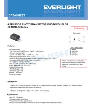
- यह डिवाइस मानक 4-पिन SSOP पैकेज में आता है। पिन कॉन्फ़िगरेशन इस प्रकार है: पिन 1: LED एनोड, पिन 2: LED कैथोड, पिन 3: फोटोट्रांजिस्टर एमिटर, पिन 4: फोटोट्रांजिस्टर कलेक्टर। क्षति को रोकने के लिए PCB लेआउट और असेंबली प्रक्रिया के दौरान सही ध्रुवीयता का ध्यान रखना आवश्यक है।
- शोर प्रतिरोध: शोर भरे वातावरण के लिए, इनपुट पिन पर डिवाइस के निकट एक छोटा बाईपास कैपेसिटर समानांतर में जोड़ना सहायक हो सकता है। आउटपुट पक्ष पर, उच्च-गति सिग्नल के लिए, परजीवी धारिता को कम करने के लिए सावधानीपूर्वक PCB लेआउट महत्वपूर्ण है।
- 7.1 अन्य ऑप्टोकपलर से अंतर
- प्रश्न: Standard grade और A/B/C grade में क्या अंतर है?
- 8. कार्य सिद्धांत और प्रौद्योगिकी रुझान
- ऑप्टोकपलर प्रौद्योगिकी का रुझान उच्च गति, कम बिजली की खपत, उच्च एकीकरण और छोटे पैकेजिंग की ओर है। हालांकि EL3H7U-G जैसे पारंपरिक फोटोट्रांजिस्टर उपकरण डीसी और कम आवृत्ति वाले अलगाव में उत्कृष्ट प्रदर्शन करते हैं, लेकिन डिजिटल आइसोलेटर जैसी नई तकनीकें उच्च डेटा दर, कम बिजली की खपत और बेहतर समय विशेषताएं प्रदान करती हैं। हालांकि, ऑप्टोकपलर उच्च कॉमन-मोड ट्रांजिएंट इम्यूनिटी, सरलता और परिपक्व उच्च वोल्टेज अलगाव सुरक्षा प्रमाणन में अपना लाभ बनाए रखते हैं, जिससे बिजली रूपांतरण और औद्योगिक नियंत्रण अनुप्रयोगों में उनकी निरंतर प्रासंगिकता सुनिश्चित होती है।
- . Mechanical, Packaging, and Assembly Information
- .1 Pin Configuration and Polarity
- .2 Soldering and Handling Guidelines
- . ऑर्डरिंग जानकारी और पैकेजिंग
- . अनुप्रयोग दिशानिर्देश और डिज़ाइन विचार
- .1 Typical Application Circuits
- .2 Key Design Considerations
- . Technical Comparison and FAQs
- .1 Differentiation from Other Photocouplers
- .2 अक्सर पूछे जाने वाले प्रश्न (FAQs)
- . कार्य सिद्धांत और प्रौद्योगिकी रुझान
- .1 Fundamental Operating Principle
- .2 Industry Trends
1. उत्पाद अवलोकन
EL3H7U-G series is a class of compact surface-mount phototransistor optocouplers (opto-isolators) designed for reliable signal isolation in modern electronic circuits. These devices play a crucial role by transmitting electrical signals via light between two isolated circuits, thereby preventing high voltages or ground loops in one circuit from affecting or damaging the other.
इसकी मूल संरचना में एक गैलियम आर्सेनाइड इन्फ्रारेड एमिटिंग डायोड और एक सिलिकॉन एनपीएन फोटोट्रांजिस्टर ऑप्टिकल युग्मन द्वारा जुड़े हुए हैं। दोनों को हरे रंग के हेलोजन-मुक्त यौगिक में एनकैप्सुलेटेड किया गया है और केवल 2.0 मिलीमीटर ऊंचाई वाले 4-पिन स्मॉल आउटलाइन पैकेज में रखा गया है। यह पैकेजिंग प्रिंटेड सर्किट बोर्ड पर सीमित स्थान वाले अनुप्रयोगों के लिए आदर्श है।
1.1 मुख्य लाभ एवं लक्षित बाजार
EL3H7U-G श्रृंखला के मुख्य लाभों में इसकी उच्च इन्सुलेशन क्षमता, कॉम्पैक्ट फॉर्म फैक्टर और अंतरराष्ट्रीय सुरक्षा एवं पर्यावरण मानकों के अनुपालन शामिल हैं। इसका 3750 Vrms इन्सुलेशन वोल्टेज संवेदनशील सर्किट को मजबूत सुरक्षा प्रदान करता है। हैलोजन-मुक्त सामग्री संरचना RoHS और REACH जैसे पर्यावरणीय नियमों का अनुपालन करती है। यह उपकरण UL, cUL, VDE, SEMKO, NEMKO, DEMKO, FIMKO और CQC जैसे प्रमुख अंतरराष्ट्रीय सुरक्षा प्रमाणन निकायों से प्रमाणित है, जो प्रमाणित घटकों की आवश्यकता वाले वैश्विक बाजारों के लिए उपयुक्त है।
इसके लक्षित अनुप्रयोग क्षेत्र विविध हैं, जो मुख्य रूप से उन क्षेत्रों पर केंद्रित हैं जहां विद्युत इन्सुलेशन और शोर प्रतिरोध क्षमता महत्वपूर्ण है। प्रमुख बाजारों में स्विचिंग मोड पावर सप्लाई, विशेष रूप से DC-DC कन्वर्टर्स, औद्योगिक प्रोग्रामेबल लॉजिक कंट्रोलर, दूरसंचार उपकरण और विभिन्न ग्राउंड पोटेंशियल या इम्पीडेंस स्तरों वाले सर्किटों के बीच सामान्य सिग्नल ट्रांसमिशन शामिल हैं।
2. गहन तकनीकी मापदंड विश्लेषण
विश्वसनीय सर्किट डिजाइन और ऑप्टोकपलर की दीर्घकालिक विश्वसनीयता सुनिश्चित करने के लिए पूर्ण अधिकतम रेटिंग और विद्युत विशेषताओं को समझना महत्वपूर्ण है।
2.1 पूर्ण अधिकतम रेटिंग
ये रेटिंग उन तनाव सीमाओं को परिभाषित करती हैं जो डिवाइस को स्थायी क्षति पहुँचा सकती हैं, और सामान्य संचालन स्थितियों के लिए लागू नहीं होती हैं।
- इनपुट पक्ष:फॉरवर्ड करंट 20 mA से अधिक नहीं होना चाहिए। रिवर्स वोल्टेज 5 V तक सीमित है, जो दर्शाता है कि यदि इनपुट रिवर्स बायस के अधीन हो सकता है, तो उचित पोलैरिटी सुरक्षा की आवश्यकता है।Fआउटपुट साइड:Rकलेक्टर करंट रेटिंग 30 mA है। कलेक्टर-एमिटर वोल्टेज 60 V तक सहन कर सकता है, जबकि एमिटर-कलेक्टर वोल्टेज बहुत कम, 5 V है, जो फोटोट्रांजिस्टर के ब्रेकडाउन गुणों की असममितता को दर्शाता है।
- थर्मल प्रदर्शन और इन्सुलेशन:डिवाइस की कुल पावर डिसिपेशन 200 mW है। इन्सुलेशन वोल्टेज 3750 Vrms है, जिसका परीक्षण नियंत्रित आर्द्रता में, पिन 1-2 और 3-4 को अलग-अलग शॉर्ट करके, 1 मिनट के लिए किया गया। ऑपरेटिंग तापमान सीमा -40°C से +125°C तक निर्धारित है।C2.2 प्रकाशविद्युत विशेषताएँCEOये पैरामीटर आमतौर पर 25°C पर मापे जाते हैं, जो सामान्य कार्य स्थितियों में डिवाइस के प्रदर्शन को परिभाषित करते हैं।ECOइनपुट विशेषताएँ:
- 1 mA की फॉरवर्ड करंट पर, फॉरवर्ड वोल्टेज का टाइपिकल मान 1.3V है, जो ड्राइवर सर्किट डिज़ाइन के लिए महत्वपूर्ण है। अधिकतम इनपुट कैपेसिटेंस 250 pF है, जो उच्च-आवृत्ति स्विचिंग प्रदर्शन को प्रभावित कर सकता है।आउटपुट विशेषताएँ:TOTकलेक्टर-एमिटर डार्क करंट बहुत कम है, जो LED बंद होने पर लीकेज करंट को दर्शाता है। निर्दिष्ट परीक्षण स्थितियों के तहत, कलेक्टर-एमिटर संतृप्ति वोल्टेज अधिकतम 0.4V है, जो दर्शाता है कि ट्रांजिस्टर के पूरी तरह से चालू होने पर वोल्टेज ड्रॉप बहुत कम है।ISOपृथक्करण पैरामीटर:
अलगाव प्रतिरोध न्यूनतम 5 x 10^10 Ω और अलगाव धारिता अधिकतम 1.0 pF है। ये मान अलगाव अवरोध के कॉमन-मोड रिजेक्शन रेशियो और उच्च-आवृत्ति शोर युग्मन को निर्धारित करने के लिए महत्वपूर्ण हैं।
2.3 ट्रांसमिशन विशेषताएँ और ग्रेडिंग सिस्टम
- करंट ट्रांसफर रेशियो ऑप्टोकपलर का सबसे महत्वपूर्ण पैरामीटर है, जिसे आउटपुट कलेक्टर करंट और इनपुट एलईडी फॉरवर्ड करंट के अनुपात के रूप में परिभाषित किया जाता है, जिसे प्रतिशत में व्यक्त किया जाता है।EL3H7U-G श्रृंखला CTR ग्रेडिंग सिस्टम का उपयोग करती है, जो डिजाइनरों को सुसंगत प्रदर्शन ग्रेड प्रदान करती है:FEL3H7U: CTR रेंज 50% से 600% तक।FEL3H7UA: CTR रेंज 100% से 200% तक।EL3H7UB: CTR रेंज 150% से 300% तक।EL3H7UC: CTR रेंज 200% से 400% तक।
- यह ग्रेडिंग अधिक सटीक डिजाइन की अनुमति देती है, विशेष रूप से उन सर्किटों में जहां लाभ स्थिरता महत्वपूर्ण है, जैसे कि पावर सप्लाई के फीडबैक लूप। स्टैंडर्ड मॉडल सबसे चौड़ी रेंज प्रदान करते हैं, जो सामान्य अनुप्रयोगों के लिए उपयुक्त हैं जहां सटीक CTR की आवश्यकता अधिक नहीं है।3. प्रदर्शन वक्र विश्लेषणCEOडेटाशीट में प्रमुख प्रदर्शन प्रवृत्तियों को दर्शाने के लिए कई ग्राफ़ प्रदान किए गए हैं। यह ध्यान रखना आवश्यक है कि ये वक्र विशिष्ट व्यवहार का प्रतिनिधित्व करते हैं और उत्पादन परीक्षण की गारंटीकृत मान नहीं हैं।CE3.1 फॉरवर्ड करंट बनाम फॉरवर्ड वोल्टेजयह ग्राफ़ विभिन्न परिवेश तापमानों पर इनपुट LED की I-V विशेषताओं को दर्शाता है। फॉरवर्ड वोल्टेज में नकारात्मक तापमान गुणांक होता है, जिसका अर्थ है कि दिए गए करंट पर, यह तापमान बढ़ने के साथ कम हो जाता है। यह डायोड का विशिष्ट व्यवहार है, जिसे थर्मल प्रबंधन और कॉन्स्टेंट करंट ड्राइव डिज़ाइन में ध्यान में रखा जाना चाहिए।3.2 कलेक्टर करंट बनाम फॉरवर्ड करंट तथा CTR बनाम फॉरवर्ड करंटFचित्र 2 दो अलग-अलग कलेक्टर-एमिटर वोल्टेज पर, आउटपुट कलेक्टर करंट और इनपुट LED करंट के बीच संबंध को दर्शाता है। कम करंट पर रैखिक संबंध है, लेकिन उच्च करंट स्तरों पर, विशेष रूप से कम कलेक्टर-एमिटर वोल्टेज पर, संतृप्ति दिखाई देती है। चित्र 3 दर्शाता है कि सामान्यीकृत CTR फॉरवर्ड करंट बढ़ने के साथ घटता है। यह इंगित करता है कि डिवाइस कम ड्राइव करंट पर सबसे अधिक कुशल होता है।C3.3 तापमान निर्भरता
- चित्र 6 दर्शाता है कि एक निश्चित फॉरवर्ड करंट पर, कलेक्टर करंट तापमान बढ़ने के साथ बढ़ता है। चित्र 7 दर्शाता है कि सामान्यीकृत CTR कमरे के तापमान के आसपास चरम पर पहुंचता है और उच्च और निम्न दोनों तापमानों पर गिर जाता है। CTR की यह तापमान निर्भरता एक महत्वपूर्ण डिजाइन कारक है। सर्किट को पूरे निर्दिष्ट तापमान रेंज में, लाभ में परिवर्तन को ध्यान में रखते हुए, ठीक से काम करने के लिए डिजाइन किया जाना चाहिए।3.4 स्विचिंग विशेषताएँIOस्विचिंग समय और लोड प्रतिरोध के बीच संबंध का ग्राफ दर्शाता है कि राइज़ टाइम और फॉल टाइम दोनों लोड प्रतिरोध के घटने के साथ घटते हैं। छोटे लोड प्रतिरोध का उपयोग तेज़ स्विचिंग गति प्राप्त करने के लिए किया जा सकता है, लेकिन इसकी कीमत आउटपुट स्टेज में अधिक बिजली की खपत के रूप में चुकानी पड़ती है। परीक्षण सर्किट में राइज़ टाइम को आउटपुट पल्स के 10% से 90% तक के समय के रूप में और फॉल टाइम को 90% से 10% तक के समय के रूप में परिभाषित किया गया है।104. Mechanical, Packaging and Assembly InformationIO4.1 Pin Configuration and Polarity
यह डिवाइस मानक 4-पिन SSOP पैकेज में आता है। पिन कॉन्फ़िगरेशन इस प्रकार है: पिन 1: LED एनोड, पिन 2: LED कैथोड, पिन 3: फोटोट्रांजिस्टर एमिटर, पिन 4: फोटोट्रांजिस्टर कलेक्टर। क्षति को रोकने के लिए PCB लेआउट और असेंबली प्रक्रिया के दौरान सही ध्रुवीयता का ध्यान रखना आवश्यक है।
4.2 सोल्डरिंग एवं हैंडलिंग दिशानिर्देशCसोल्डरिंग तापमान का पूर्ण अधिकतम रेटेड मान 260°C, 10 सेकंड के लिए है। यह सामान्य लीड-फ्री रीफ्लो प्रोफाइल के अनुरूप है। नमी-संवेदनशील उपकरणों के लिए IPC/JEDEC J-STD-020 के मानक दिशानिर्देशों का पालन किया जाना चाहिए। उपकरण को उसके मूल डिसिकेंट युक्त नमी-रोधी बैग में संग्रहित किया जाना चाहिए और नियंत्रित परिस्थितियों में रखा जाना चाहिए; यदि बैग खोला गया है या एक्सपोजर समय सीमा से अधिक हो गया है, तो सोल्डरिंग से पहले बेकिंग की जानी चाहिए।F5. ऑर्डर जानकारी एवं पैकेजिंगCFपार्ट नंबर संरचना है: EL3H7U(X)(Y)-VG।
X: CTR ग्रेड।
- Y: रील पैकेजिंग विकल्प। TA और TB संभवतः विभिन्न रील आकार या पैकेजिंग दिशा को संदर्भित करते हैं, प्रत्येक रील में 5000 उपकरण शामिल होते हैं।V: वैकल्पिक VDE प्रमाणन चिह्न।FG: हैलोजन-मुक्त सामग्री को दर्शाता है।CEउदाहरण: EL3H7UB-TA-VG एक ग्रेड B CTR उपकरण को दर्शाता है, जो TA रील पैकेजिंग में है, VDE प्रमाणित है और हैलोजन-मुक्त सामग्री से बना है।
- 6. अनुप्रयोग मार्गदर्शिका और डिज़ाइन विचार6.1 विशिष्ट अनुप्रयोग सर्किट
- इसका मुख्य अनुप्रयोग सिग्नल अलगाव है। एक विशिष्ट सर्किट में एक करंट-सीमित रोकनेवाला के माध्यम से डिजिटल सिग्नल स्रोत से इनपुट LED को चलाना शामिल है। आउटपुट फोटोट्रांजिस्टर का उपयोग उलटा आउटपुट सिग्नल उत्पन्न करने के लिए कॉमन-एमिटर कॉन्फ़िगरेशन में, या इन-फेज सिग्नल उत्पन्न करने के लिए एमिटर-फॉलोअर कॉन्फ़िगरेशन में किया जा सकता है।6.2 प्रमुख डिज़ाइन विचार
- LED ड्राइव करंट: आवश्यक स्विचिंग गति और CTR के आधार पर फॉरवर्ड करंट चुनें। कम करंट उच्च CTR प्रदान करता है लेकिन स्विचिंग गति धीमी होती है। श्रृंखला प्रतिरोध की गणना करने के लिए सूत्र का उपयोग करना आवश्यक है।आउटपुट लोड रेसिस्टेंस: यह रेसिस्टेंस आउटपुट वोल्टेज स्विंग, स्विचिंग गति और बिजली की खपत निर्धारित करता है। छोटा रेसिस्टेंस तेज़ स्विचिंग गति प्रदान करता है, लेकिन आउटपुट वोल्टेज स्विंग कम होता है और कलेक्टर करंट अधिक होता है।
CTR क्षय: ऑप्टोकपलर का CTR समय के साथ कम होता है, खासकर उच्च तापमान और उच्च LED करंट पर काम करने पर। लंबी आयु वाले डिज़ाइन के लिए, ऑपरेटिंग करंट को डीरेट करना चाहिए और पर्याप्त थर्मल प्रबंधन सुनिश्चित करना चाहिए।
शोर प्रतिरोध: शोर भरे वातावरण के लिए, इनपुट पिन पर डिवाइस के निकट एक छोटा बाईपास कैपेसिटर समानांतर में जोड़ना सहायक हो सकता है। आउटपुट पक्ष पर, उच्च-गति सिग्नल के लिए, परजीवी धारिता को कम करने के लिए सावधानीपूर्वक PCB लेआउट महत्वपूर्ण है।
7. तकनीकी तुलना और सामान्य प्रश्न
7.1 अन्य ऑप्टोकपलर से अंतर
EL3H7U-G श्रृंखला अपने कॉम्पैक्ट SSOP पैकेज, उच्च 3750 Vrms इंसुलेशन रेटिंग, -40°C से +125°C तक के व्यापक ऑपरेटिंग तापमान और व्यापक अंतरराष्ट्रीय सुरक्षा प्रमाणन संयोजन के माध्यम से अलग दिखती है। कई प्रतिस्पर्धी उपकरण समान CTR या गति प्रदान कर सकते हैं, लेकिन पूर्ण प्रमाणन सेट या उच्च तापमान क्षमता का अभाव होता है।F7.2 अक्सर पूछे जाने वाले प्रश्न
प्रश्न: Standard grade और A/B/C grade में क्या अंतर है?
उत्तर: मानक ग्रेड का CTR दायरा बहुत व्यापक होता है। A, B और C ग्रेड को संकीर्ण, गारंटीकृत CTR दायरों में वर्गीकृत किया गया है। पूर्वानुमेय लाभ की आवश्यकता वाले डिज़ाइनों के लिए, ग्रेडेड उपकरणों का उपयोग करें।Cप्रश्न: क्या मैं इसे AC इनपुट सिग्नल अलगाव के लिए उपयोग कर सकता हूँ?Fउत्तर: सीधे उपयोग नहीं किया जा सकता। इनपुट एक LED है, जो एक डायोड है और केवल एक दिशा में संचालित होता है। AC सिग्नल को अलग करने के लिए, पहले उसे रेक्टिफाई करना होगा या समर्पित AC इनपुट ऑप्टोकपलर का उपयोग करना होगा।CEप्रश्न: अधिकतम डेटा दर की गणना कैसे करें?Fउत्तर: अधिकतम डेटा दर राइज़ टाइम और फॉल टाइम के योग द्वारा सीमित होती है। डिजिटल सिग्नल के लिए एक मोटा अनुमान है: बैंडविड्थ ≈ 0.35 / राइज़ टाइम। एक विशिष्ट राइज़ टाइम पर, बैंडविड्थ लगभग 44 kHz होती है। विश्वसनीय डिजिटल संचार के लिए, वास्तविक डेटा दर इससे कम होगी।CEप्रश्न: आइसोलेशन कैपेसिटेंस महत्वपूर्ण क्यों है?Fउत्तर: उच्च-आवृत्ति कॉमन-मोड शोर को दबाने के लिए कम आइसोलेशन कैपेसिटेंस महत्वपूर्ण है। ऐसे अनुप्रयोगों में जहां आइसोलेशन बैरियर के पार तेज वोल्टेज ट्रांजिएंट होते हैं, उच्च आइसोलेशन कैपेसिटेंस शोर को प्राइमरी साइड से सेकेंडरी साइड में युग्मित कर सकता है, जिससे विफलता हो सकती है।
8. कार्य सिद्धांत और प्रौद्योगिकी रुझान
8.1 मूल सिद्धांतCऑप्टोकपलर विद्युत-प्रकाश-विद्युत रूपांतरण के सिद्धांत पर कार्य करता है। इनपुट पर लगाया गया विद्युत संकेत LED को धारा के समानुपाती अवरक्त प्रकाश उत्सर्जित करने के लिए प्रेरित करता है। यह प्रकाश पैकेज के भीतर एक पारदर्शी पृथक्करण अवरोध को पार करता है। आउटपुट पर, एक फोटोट्रांजिस्टर इस प्रकाश का पता लगाता है, जिससे बेस करंट उत्पन्न होता है, जो बदले में एक बड़े कलेक्टर करंट को नियंत्रित करता है। दोनों सर्किट विद्युत रूप से पृथक होते हैं और केवल प्रकाश द्वारा युग्मित होते हैं।F8.2 उद्योग रुझान
ऑप्टोकपलर प्रौद्योगिकी का रुझान उच्च गति, कम बिजली की खपत, उच्च एकीकरण और छोटे पैकेजिंग की ओर है। हालांकि EL3H7U-G जैसे पारंपरिक फोटोट्रांजिस्टर उपकरण डीसी और कम आवृत्ति वाले अलगाव में उत्कृष्ट प्रदर्शन करते हैं, लेकिन डिजिटल आइसोलेटर जैसी नई तकनीकें उच्च डेटा दर, कम बिजली की खपत और बेहतर समय विशेषताएं प्रदान करती हैं। हालांकि, ऑप्टोकपलर उच्च कॉमन-मोड ट्रांजिएंट इम्यूनिटी, सरलता और परिपक्व उच्च वोल्टेज अलगाव सुरक्षा प्रमाणन में अपना लाभ बनाए रखते हैं, जिससे बिजली रूपांतरण और औद्योगिक नियंत्रण अनुप्रयोगों में उनकी निरंतर प्रासंगिकता सुनिश्चित होती है।
स्विचिंग समय बनाम लोड प्रतिरोध (RL) का ग्राफ दर्शाता है कि राइज टाइम (tr) और फॉल टाइम (tf) दोनों लोड प्रतिरोध के कम होने के साथ घटते हैं। छोटे लोड रेसिस्टर्स के साथ तेज स्विचिंग प्राप्त की जाती है, लेकिन इसकी कीमत आउटपुट स्टेज में उच्च बिजली अपव्यय के रूप में चुकानी पड़ती है। टेस्ट सर्किट (चित्र 13) trआउटपुट पल्स के 10% से 90% तक का समय और tf90% से 10% तक के रूप में।
. Mechanical, Packaging, and Assembly Information
.1 Pin Configuration and Polarity
डिवाइस एक मानक 4-पिन SSOP फुटप्रिंट का उपयोग करता है। पिनआउट इस प्रकार है: पिन 1: IRED का एनोड, पिन 2: IRED का कैथोड, पिन 3: फोटोट्रांजिस्टर का एमिटर, पिन 4: फोटोट्रांजिस्टर का कलेक्टर। क्षति को रोकने के लिए PCB लेआउट और असेंबली के दौरान सही पोलैरिटी का पालन किया जाना चाहिए।
.2 Soldering and Handling Guidelines
सोल्डरिंग तापमान (TSOL) के लिए पूर्ण अधिकतम रेटिंग 10 सेकंड के लिए 260°C है।SOLयह सामान्य लीड-मुक्त रीफ्लो सोल्डरिंग प्रोफाइल के अनुरूप है। नमी-संवेदनशील उपकरणों के लिए मानक IPC/JEDEC J-STD-020 दिशानिर्देशों का पालन किया जाना चाहिए। उपकरण को नियंत्रित परिस्थितियों में डिसिकेंट के साथ अपनी मूल नमी-अवरोधक बैग में संग्रहित किया जाना चाहिए और यदि बैग खोला गया है या एक्सपोजर समय सीमा से अधिक हो गया है तो सोल्डरिंग से पहले बेक किया जाना चाहिए।
. ऑर्डरिंग जानकारी और पैकेजिंग
पार्ट नंबर इस संरचना का अनुसरण करता है: EL3H7U(X)(Y)-VG.
- X:CTR रैंक (A, B, C, या मानक ग्रेड के लिए रिक्त)।
- Y:टेप और रील विकल्प (TA, TB, या रिक्त)। TA और TB संभवतः विभिन्न रील आकारों या पैकेजिंग अभिविन्यासों को संदर्भित करते हैं, दोनों में प्रति रील 5000 इकाइयाँ होती हैं।
- V:वैकल्पिक VDE अनुमोदन चिह्न।
- G:हैलोजन-मुक्त सामग्री को दर्शाता है।
उदाहरण: EL3H7UB-TA-VG एक B-ग्रेड CTR डिवाइस होगा, TA टेप और रील पर पैकेज्ड, VDE अनुमोदन और हैलोजन-मुक्त सामग्री के साथ।
. अनुप्रयोग दिशानिर्देश और डिज़ाइन विचार
.1 Typical Application Circuits
प्राथमिक अनुप्रयोग सिग्नल अलगाव है। एक विशिष्ट सर्किट में डिजिटल सिग्नल स्रोत (जैसे, माइक्रोकंट्रोलर GPIO) से करंट-लिमिटिंग रेसिस्टर के साथ इनपुट LED को ड्राइव करना शामिल है। आउटपुट फोटोट्रांजिस्टर का उपयोग इनवर्टेड आउटपुट सिग्नल उत्पन्न करने के लिए कॉमन-एमिटर कॉन्फ़िगरेशन (कलेक्टर पुल-अप रेसिस्टर से जुड़ा, एमिटर ग्राउंडेड) में, या नॉन-इनवर्टेड सिग्नल के लिए एमिटर-फॉलोअर कॉन्फ़िगरेशन में किया जा सकता है।
.2 Key Design Considerations
- एलईडी ड्राइव करंट:I का चयन करेंFआवश्यक स्विचिंग गति और CTR के आधार पर। कम IFउच्च CTR प्रदान करता है लेकिन धीमी स्विचिंग। एक श्रृंखला रोकनेवाला की गणना R = (V का उपयोग करके की जानी चाहिएस्रोत- VF) / IF.
- Output Load Resistor (RL):यह रेसिस्टर आउटपुट वोल्टेज स्विंग, स्विचिंग स्पीड और पावर डिसिपेशन सेट करता है। एक छोटा RLतेज स्विचिंग देता है लेकिन कम आउटपुट वोल्टेज स्विंग और उच्च IC.
- CTR Degradation:फोटोकपलर का CTR समय के साथ कम हो सकता है, खासकर जब उच्च तापमान और उच्च LED धारा पर संचालित किया जाता है। लंबी आयु वाले डिजाइनों के लिए, संचालन I को डीरेट करेंFऔर पर्याप्त थर्मल प्रबंधन सुनिश्चित करें।
- नॉइज़ इम्यूनिटी:शोरगुल वाले वातावरण के लिए, इनपुट पिनों के पार, डिवाइस के निकट, एक छोटा बाईपास कैपेसिटर (जैसे, 0.1 μF) मदद कर सकता है। आउटपुट पर, उच्च-गति सिग्नल के लिए स्ट्रे कैपेसिटेंस को कम करने के लिए सावधानीपूर्वक PCB लेआउट महत्वपूर्ण है।
. Technical Comparison and FAQs
.1 Differentiation from Other Photocouplers
EL3H7U-G श्रृंखला अपने कॉम्पैक्ट SSOP पैकेज, उच्च 3750 Vrms इन्सुलेशन रेटिंग, व्यापक -40°C से +125°C ऑपरेटिंग तापमान और व्यापक अंतरराष्ट्रीय सुरक्षा प्रमाणनों के संयोजन के माध्यम से स्वयं को अलग करती है। कई प्रतिस्पर्धी उपकरण समान CTR या गति प्रदान कर सकते हैं, लेकिन उनमें अनुमोदनों का पूरा सेट या उच्च-तापमान क्षमता का अभाव हो सकता है।
.2 अक्सर पूछे जाने वाले प्रश्न (FAQs)
प्र: मानक ग्रेड और A/B/C ग्रेड के बीच क्या अंतर है?
A: मानक ग्रेड में बहुत व्यापक CTR रेंज (50-600%) होती है। A, B, और C ग्रेड को अधिक सख्त, गारंटीकृत CTR रेंज (जैसे, C-ग्रेड के लिए 200-400%) में बांटा गया है। पूर्वानुमेय लाभ की आवश्यकता वाले डिज़ाइनों के लिए ग्रेडेड पार्ट्स का उपयोग करें।
Q: क्या मैं इसे AC इनपुट सिग्नल आइसोलेशन के लिए उपयोग कर सकता हूं?
A: सीधे नहीं। इनपुट एक IRED है, जो एक डायोड है और केवल एक दिशा में संचालित होता है। एक AC सिग्नल को आइसोलेट करने के लिए, आपको पहले इसे रेक्टिफाई करना होगा या एक समर्पित AC-इनपुट फोटोकपलर का उपयोग करना होगा।
Q: मैं अधिकतम डेटा दर की गणना कैसे करूं?
A>The maximum data rate is limited by the sum of the rise and fall times (tr+ tf) के योग द्वारा सीमित होती है। एक डिजिटल सिग्नल के लिए एक मोटा अनुमान है: बैंडविड्थ ≈ 0.35 / (tr). विशिष्ट tr8 μs के समय के लिए, बैंडविड्थ लगभग 44 kHz है। विश्वसनीय डिजिटल संचार के लिए, व्यावहारिक डेटा दर इससे कम होगी।
Q: अलगाव कैपेसिटेंस महत्वपूर्ण क्यों है?
A: कम अलगाव कैपेसिटेंस (CIO) उच्च-आवृत्ति कॉमन-मोड शोर को रद्द करने के लिए महत्वपूर्ण है। इन्सुलेशन बैरियर के पार तेज वोल्टेज ट्रांजिएंट वाले अनुप्रयोगों में (जैसे मोटर ड्राइव में), एक उच्च CIOप्राथमिक से द्वितीयक पक्ष में शोर को युग्मित कर सकता है, जिससे संभावित रूप से खराबी हो सकती है।
. कार्य सिद्धांत और प्रौद्योगिकी रुझान
.1 Fundamental Operating Principle
एक फोटोकपलर विद्युत-प्रकाशिक-विद्युत रूपांतरण के सिद्धांत पर कार्य करता है। इनपुट साइड पर लगाया गया एक विद्युत संकेत IRED को धारा के समानुपाती अवरक्त प्रकाश उत्सर्जित करने के लिए प्रेरित करता है। यह प्रकाश पैकेज के भीतर एक पारदर्शी पृथक्करण अवरोध को पार करता है। आउटपुट साइड पर, फोटोट्रांजिस्टर इस प्रकाश का पता लगाता है, जिससे एक बेस करंट उत्पन्न होता है जो बदले में एक बहुत बड़े कलेक्टर करंट को नियंत्रित करता है। दोनों सर्किट विद्युत रूप से पृथक होते हैं, उनके बीच केवल प्रकाशीय युग्मन होता है।
.2 Industry Trends
फोटोकपलर प्रौद्योगिकी में प्रवृत्ति उच्च गति, कम बिजली की खपत, उच्च एकीकरण और छोटे पैकेजों की ओर है। जबकि EL3H7U-G जैसे पारंपरिक फोटोट्रांजिस्टर-आधारित उपकरण DC और कम-आवृत्ति वाली अलगाव के लिए उत्कृष्ट हैं, नई प्रौद्योगिकियाँ जैसे डिजिटल आइसोलेटर (CMOS और RF या कैपेसिटिव कपलिंग का उपयोग करके) काफी उच्च डेटा दर, कम बिजली और बेहतर समय विशेषताएँ प्रदान करती हैं। हालाँकि, फोटोकपलर उच्च कॉमन-मोड ट्रांजिएंट इम्यूनिटी (CMTI), सरलता और उच्च-वोल्टेज अलगाव के लिए स्थापित सुरक्षा प्रमाणपत्रों में लाभ बनाए रखते हैं, जिससे पावर रूपांतरण और औद्योगिक नियंत्रण अनुप्रयोगों में उनकी निरंतर प्रासंगिकता सुनिश्चित होती है।
LED विनिर्देश शब्दावली का विस्तृत विवरण
LED तकनीकी शब्दावली की पूर्ण व्याख्या
1. प्रकाशविद्युत प्रदर्शन के मुख्य संकेतक
| शब्दावली | Unit/Representation | Layman's Explanation | Why It Is Important |
|---|---|---|---|
| दीप्ति दक्षता (Luminous Efficacy) | lm/W (लुमेन प्रति वाट) | प्रति वाट विद्युत ऊर्जा से उत्पन्न प्रकाश प्रवाह, जितना अधिक होगा उतनी अधिक ऊर्जा बचत होगी। | यह सीधे तौर पर प्रकाश साधन की ऊर्जा दक्षता श्रेणी और बिजली लागत निर्धारित करता है। |
| Luminous Flux | lm (लुमेन) | प्रकाश स्रोत द्वारा उत्सर्जित कुल प्रकाश मात्रा, जिसे आम बोलचाल में "चमक" कहा जाता है। | यह निर्धारित करना कि लैंप पर्याप्त रोशनी दे रहा है या नहीं। |
| दीप्ति कोण (Viewing Angle) | ° (डिग्री), जैसे 120° | वह कोण जब प्रकाश की तीव्रता आधी रह जाती है, जो बीम की चौड़ाई निर्धारित करता है। | प्रकाश के कवरेज क्षेत्र और एकरूपता को प्रभावित करता है। |
| Color Temperature (CCT) | K (Kelvin), e.g., 2700K/6500K | प्रकाश का रंग गर्म या ठंडा होता है; कम मान पीला/गर्म, उच्च मान सफेद/ठंडा दर्शाता है। | प्रकाश व्यवस्था का वातावरण और उपयुक्त परिदृश्य निर्धारित करता है। |
| रंग प्रतिपादन सूचकांक (CRI / Ra) | इकाईहीन, 0–100 | प्रकाश स्रोत द्वारा वस्तुओं के वास्तविक रंगों को पुनः प्रस्तुत करने की क्षमता, Ra≥80 उत्तम माना जाता है। | रंगों की वास्तविकता को प्रभावित करता है, शॉपिंग मॉल, आर्ट गैलरी जैसे उच्च आवश्यकता वाले स्थानों में प्रयुक्त। |
| Color Tolerance (SDCM) | MacAdam Ellipse Steps, e.g., "5-step" | रंग एकरूपता का मात्रात्मक मापदंड, चरण संख्या जितनी कम होगी, रंग उतना ही अधिक एकसमान होगा। | एक ही बैच के दीपकों के रंग में कोई अंतर न हो, यह सुनिश्चित करना। |
| प्रमुख तरंगदैर्ध्य (Dominant Wavelength) | nm (नैनोमीटर), उदाहरणार्थ 620nm (लाल) | रंगीन LED रंगों के संगत तरंगदैर्ध्य मान। | लाल, पीले, हरे आदि मोनोक्रोमैटिक एलईडी के रंग टोन (ह्यू) का निर्धारण करें। |
| स्पेक्ट्रम वितरण (Spectral Distribution) | तरंगदैर्ध्य बनाम तीव्रता वक्र | LED द्वारा उत्सर्जित प्रकाश की विभिन्न तरंगदैर्ध्य पर तीव्रता वितरण प्रदर्शित करता है। | रंग प्रतिपादन एवं रंग गुणवत्ता को प्रभावित करता है। |
दो, विद्युत मापदंड
| शब्दावली | प्रतीक | Layman's Explanation | डिज़ाइन विचार |
|---|---|---|---|
| फॉरवर्ड वोल्टेज (Forward Voltage) | Vf | LED को प्रकाशित करने के लिए आवश्यक न्यूनतम वोल्टेज, "स्टार्ट-अप थ्रेशोल्ड" के समान। | ड्राइविंग पावर सप्लाई वोल्टेज ≥ Vf होना चाहिए, कई LEDs को श्रृंखला में जोड़ने पर वोल्टेज जुड़ जाता है। |
| Forward Current | If | एलईडी को सामान्य रूप से चमकने के लिए आवश्यक करंट मान। | स्थिर धारा ड्राइव का उपयोग आमतौर पर किया जाता है, धारा चमक और जीवनकाल निर्धारित करती है। |
| अधिकतम पल्स धारा (Pulse Current) | Ifp | डिमिंग या फ्लैश के लिए अल्पावधि में सहन करने योग्य पीक करंट। | पल्स चौड़ाई और ड्यूटी साइकल को सख्ती से नियंत्रित किया जाना चाहिए, अन्यथा अत्यधिक गर्मी से क्षति होगी। |
| रिवर्स वोल्टेज (Reverse Voltage) | Vr | LED द्वारा सहन की जा सकने वाली अधिकतम रिवर्स वोल्टेज, जिससे अधिक होने पर उसके ब्रेकडाउन होने की संभावना है। | सर्किट में रिवर्स कनेक्शन या वोल्टेज स्पाइक से सुरक्षा आवश्यक है। |
| Thermal Resistance | Rth (°C/W) | चिप से सोल्डर पॉइंट तक गर्मी के प्रवाह का प्रतिरोध, कम मान बेहतर ऊष्मा अपव्यय को दर्शाता है। | उच्च तापीय प्रतिरोध के लिए मजबूत ऊष्मा अपव्यय डिज़ाइन की आवश्यकता होती है, अन्यथा जंक्शन तापमान बढ़ जाता है। |
| इलेक्ट्रोस्टैटिक डिस्चार्ज सहनशीलता (ESD Immunity) | V (HBM), जैसे 1000V | एंटीस्टैटिक शॉक प्रतिरोध, उच्च मूल्य इलेक्ट्रोस्टैटिक क्षति के प्रति कम संवेदनशीलता दर्शाता है। | उत्पादन में इलेक्ट्रोस्टैटिक सुरक्षा उपायों का पालन आवश्यक है, विशेष रूप से उच्च संवेदनशीलता वाले LED के लिए। |
तीन, थर्मल प्रबंधन और विश्वसनीयता
| शब्दावली | प्रमुख संकेतक | Layman's Explanation | प्रभाव |
|---|---|---|---|
| जंक्शन तापमान (Junction Temperature) | Tj (°C) | LED चिप का आंतरिक वास्तविक कार्य तापमान। | प्रत्येक 10°C कमी पर, जीवनकाल दोगुना हो सकता है; अत्यधिक तापमान से प्रकाश क्षय और रंग विस्थापन होता है। |
| Lumen Depreciation | L70 / L80 (घंटे) | चमक प्रारंभिक मान के 70% या 80% तक गिरने में लगने वाला समय। | LED की "सेवा जीवन" को सीधे परिभाषित करना। |
| लुमेन रखरखाव दर (Lumen Maintenance) | % (जैसे 70%) | एक निश्चित अवधि के उपयोग के बाद शेष चमक का प्रतिशत। | दीर्घकालिक उपयोग के बाद चमक बनाए रखने की क्षमता को दर्शाता है। |
| Color Shift | Δu′v′ या मैकएडम एलिप्स | उपयोग के दौरान रंग में परिवर्तन की मात्रा। | प्रकाश दृश्यों के रंग स्थिरता को प्रभावित करता है। |
| Thermal Aging | सामग्री के प्रदर्शन में गिरावट | लंबे समय तक उच्च तापमान के कारण एनकैप्सुलेशन सामग्री का क्षरण। | इससे चमक में कमी, रंग परिवर्तन या ओपन सर्किट विफलता हो सकती है। |
चतुर्थ, एनकैप्सुलेशन एवं सामग्री
| शब्दावली | सामान्य प्रकार | Layman's Explanation | विशेषताएँ एवं अनुप्रयोग |
|---|---|---|---|
| पैकेजिंग प्रकार | EMC, PPA, सिरेमिक | चिप की सुरक्षा करने वाली और प्रकाशिक एवं ऊष्मीय इंटरफेस प्रदान करने वाली आवरण सामग्री। | EMC उच्च ताप सहनशीलता, कम लागत; सिरेमिक उत्कृष्ट ताप अपव्यय, लंबी आयु। |
| चिप संरचना | फॉरवर्ड-माउंटेड, फ्लिप चिप (Flip Chip) | चिप इलेक्ट्रोड व्यवस्था विधि। | फ्लिप-चिप तकनीक बेहतर हीट डिसिपेशन और उच्च प्रकाश दक्षता प्रदान करती है, जो उच्च शक्ति अनुप्रयोगों के लिए उपयुक्त है। |
| फॉस्फर कोटिंग | YAG, सिलिकेट, नाइट्राइड | नीले प्रकाश चिप पर लगाया जाता है, जिसका कुछ भाग पीले/लाल प्रकाश में परिवर्तित होकर सफेद प्रकाश बनाता है। | विभिन्न फॉस्फोर प्रकाश दक्षता, कलर टेम्परेचर और कलर रेंडरिंग इंडेक्स को प्रभावित करते हैं। |
| लेंस/ऑप्टिकल डिज़ाइन | प्लानर, माइक्रोलेंस, टोटल इंटरनल रिफ्लेक्शन | पैकेजिंग सतह की ऑप्टिकल संरचना, प्रकाश वितरण को नियंत्रित करती है। | उत्सर्जन कोण और प्रकाश वितरण वक्र निर्धारित करता है। |
5. गुणवत्ता नियंत्रण और ग्रेडिंग
| शब्दावली | बिनिंग सामग्री | Layman's Explanation | उद्देश्य |
|---|---|---|---|
| ल्यूमिनस फ्लक्स बिनिंग | कोड जैसे 2G, 2H | चमक के स्तर के अनुसार समूहीकरण, प्रत्येक समूह का न्यूनतम/अधिकतम लुमेन मान होता है। | एक ही बैच के उत्पादों की चमक सुनिश्चित करें। |
| वोल्टेज ग्रेडिंग | कोड जैसे 6W, 6X | फॉरवर्ड वोल्टेज रेंज के अनुसार समूहीकृत करें। | ड्राइविंग पावर स्रोत के मिलान और सिस्टम दक्षता में सुधार के लिए सुविधाजनक। |
| रंग वर्गीकरण | 5-step MacAdam ellipse | रंग निर्देशांक के अनुसार समूहीकरण करें, यह सुनिश्चित करते हुए कि रंग बहुत छोटी सीमा के भीतर आते हैं। | रंग एकरूपता सुनिश्चित करें, एक ही प्रकाश साधन के भीतर रंग में असमानता से बचें। |
| रंग तापमान श्रेणीकरण | 2700K, 3000K, आदि। | रंग तापमान के अनुसार समूहीकृत किया गया है, प्रत्येक समूह की अपनी संबंधित निर्देशांक सीमा है। | विभिन्न परिदृश्यों की रंग तापमान आवश्यकताओं को पूरा करना। |
छह, परीक्षण और प्रमाणन
| शब्दावली | मानक/परीक्षण | Layman's Explanation | अर्थ |
|---|---|---|---|
| LM-80 | लुमेन रखरखाव परीक्षण | Long-term illumination under constant temperature conditions, recording brightness attenuation data. | Used to estimate LED lifespan (combined with TM-21). |
| TM-21 | जीवन प्रक्षेपण मानक | LM-80 डेटा के आधार पर वास्तविक उपयोग की स्थितियों में जीवनकाल का अनुमान लगाना। | वैज्ञानिक जीवनकाल पूर्वानुमान प्रदान करना। |
| IESNA मानक | Illuminating Engineering Society Standards | Optical, electrical, and thermal test methods are covered. | Industry-recognized testing basis. |
| RoHS / REACH | पर्यावरण प्रमाणन | उत्पाद में हानिकारक पदार्थ (जैसे सीसा, पारा) नहीं होने का सुनिश्चित करें। | अंतर्राष्ट्रीय बाजार में प्रवेश की पात्रता शर्तें। |
| ENERGY STAR / DLC | ऊर्जा दक्षता प्रमाणन | प्रकाश उत्पादों के लिए ऊर्जा दक्षता और प्रदर्शन प्रमाणन। | यह सरकारी खरीद और सब्सिडी परियोजनाओं में आमतौर पर उपयोग किया जाता है, जिससे बाजार प्रतिस्पर्धा बढ़ती है। |