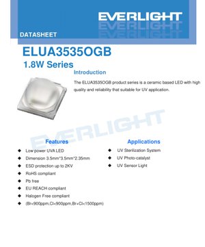
1. उत्पाद अवलोकन
ELUA3535OGB उत्पाद श्रृंखला एक उच्च-विश्वसनीयता, सिरेमिक-आधारित एलईडी समाधान का प्रतिनिधित्व करती है जिसे विशेष रूप से पराबैंगनी (यूवीए) अनुप्रयोगों के लिए इंजीनियर किया गया है। इसकी मूल संरचना Al2O3 (एल्यूमीनियम ऑक्साइड) सिरेमिक सब्सट्रेट का उपयोग करती है, जो पारंपरिक प्लास्टिक पैकेजों की तुलना में श्रेष्ठ थर्मल प्रबंधन प्रदान करता है, जिससे चुनौतीपूर्ण परिस्थितियों में बढ़ी हुई दीर्घायु और स्थिर प्रदर्शन प्राप्त होता है।
मुख्य लाभ: The primary benefits of this series include its robust सिरैमिक पैकेज for excellent heat dissipation, integrated ESD protection up to 2KV (Human Body Model), and compliance with major environmental and safety standards including RoHS, Pb-free, EU REACH, and halogen-free requirements (Br<900ppm, Cl<900ppm, Br+Cl<1500ppm). The 120-degree viewing angle offers a broad radiation pattern suitable for area illumination tasks.
Target Market & Applications: यह एलईडी औद्योगिक और वाणिज्यिक यूवी अनुप्रयोगों के लिए डिज़ाइन की गई है जहां विश्वसनीयता और प्रकाशीय आउटपुट महत्वपूर्ण हैं। प्रमुख अनुप्रयोग क्षेत्रों में वायु और जल शुद्धिकरण के लिए यूवी कीटाणुशोधन प्रणालियाँ, सतह उपचार और गंध उन्मूलन के लिए यूवी फोटोकैटलिस्ट सिस्टम, और यूवी सेंसर तथा क्योरिंग प्रक्रियाओं के लिए प्रकाश स्रोत के रूप में उपयोग शामिल हैं।
2. तकनीकी पैरामीटर गहन विश्लेषण
2.1 Absolute Maximum Ratings
ये रेटिंग उन सीमाओं को परिभाषित करती हैं जिनके परे डिवाइस को स्थायी क्षति हो सकती है। इन स्थितियों में संचालन की गारंटी नहीं है।
- Max. DC Forward Current (IF): 385nm, 395nm, और 405nm वेरिएंट के लिए 1000 mA। 365nm वेरिएंट के लिए, अधिकतम करंट 700 mA तक कम कर दिया गया है, जो इसकी भिन्न अर्धचालक सामग्री विशेषताओं और तापीय संवेदनशीलता को दर्शाता है।
- Max. ESD Resistance (VB): 2000 V (HBM), जो हैंडलिंग के लिए अच्छी मजबूती प्रदान करता है।
- Thermal Resistance (Rth): 4 °C/W. यह कम मान, जो सिरेमिक पैकेज के कारण है, एलईडी जंक्शन से थर्मल पैड तक प्रभावी ऊष्मा स्थानांतरण को दर्शाता है।
- Max. Junction Temperature (TJ): 125 °C.
- Operating & Storage Temperature: -10 to +100 °C for operation, and -40 to +100 °C for storage.
2.2 Photometric & Electrical Characteristics
तालिका 500mA के एक मानक परीक्षण धारा और 25°C के थर्मल पैड तापमान पर विभिन्न तरंगदैर्ध्य बिन के लिए प्रमुख प्रदर्शन मापदंडों को सूचीबद्ध करती है।
- पीक वेवलेंथ: चार बिन में उपलब्ध: 360-370nm (U36), 380-390nm (U38), 390-400nm (U39), और 400-410nm (U40)।
- Radiant Flux: Minimum radiant flux is specified at 1000mW (U2 bin), with typical values around 1250mW and maximum up to 1500mW across all wavelength groups.
- Forward Voltage (VF): Ranges from 3.2V to 4.0V at 500mA, categorized into specific voltage bins (e.g., 3.2-3.4V, 3.4-3.6V).
3. Binning System Explanation
उत्पाद को स्थिरता सुनिश्चित करने और अनुप्रयोग आवश्यकताओं के आधार पर सटीक चयन की अनुमति देने के लिए बिन में वर्गीकृत किया जाता है।
3.1 Radiant Flux Binning
रेडिएंट फ्लक्स IF=500mA पर ±10% सहनशीलता के साथ मापा जाता है। बिन हैं:
- U2: 1000mW से 1200mW
- U3: 1200mW से 1400mW
- U4: 1400mW से 1500mW
3.2 Peak Wavelength Binning
शिखर तरंगदैर्ध्य ±1nm की सहनशीलता के साथ मापा जाता है। समूह (U36, U38, U39, U40) खंड 2.2 में सूचीबद्ध तरंगदैर्ध्य सीमाओं के अनुरूप हैं।
3.3 फॉरवर्ड वोल्टेज बिनिंग
फॉरवर्ड वोल्टेज को IF=500mA पर ±2% की सहनशीलता के साथ मापा जाता है। बिन (3234, 3436, 3638, 3840) न्यूनतम और अधिकतम V को परिभाषित करते हैं।F रेंज (उदाहरण के लिए, 3234 = 3.2V से 3.4V).
4. प्रदर्शन वक्र विश्लेषण
4.1 Spectrum & Relative Radiant Flux vs. Current
स्पेक्ट्रल ग्राफ 365nm, 385nm, 395nm, और 405nm वेरिएंट के लिए विशिष्ट उत्सर्जन वक्र दिखाते हैं। वक्र संकीर्ण बैंड वाले हैं, जो यूवी एलईडी की विशेषता है। रिलेटिव रेडिएंट फ्लक्स बनाम फॉरवर्ड करंट ग्राफ रेटेड करंट तक लगभग रैखिक संबंध प्रदर्शित करता है, जिसमें 405nm एलईडी आम तौर पर उच्चतम सापेक्ष आउटपुट दिखाती है, उसके बाद समान करंट स्तर पर 395nm, 385nm, और 365nm का स्थान आता है।
4.2 Peak Wavelength & फॉरवर्ड वोल्टेज vs. Current
The Peak Wavelength vs. फॉरवर्ड करंट plot shows minimal shift (<5nm) across the operating current range for all wavelengths, indicating good spectral stability. The फॉरवर्ड वोल्टेज vs. फॉरवर्ड करंट curve shows the typical diode exponential characteristic, with VF करंट के साथ बढ़ रहा है। 365nm एलईडी आमतौर पर थोड़ा अधिक V प्रदर्शित करती हैF लंबी तरंगदैर्ध्य वाले प्रकारों की तुलना में।
4.3 तापमान निर्भरता
रिलेटिव रेडिएंट फ्लक्स बनाम एंबिएंट टेम्परेचर ग्राफ दर्शाता है कि तापमान बढ़ने पर आउटपुट कम होता है, जो एलईडी के लिए एक सामान्य व्यवहार है। डीरेटिंग कर्व डिजाइन के लिए महत्वपूर्ण है: यह किसी दिए गए परिवेश के तापमान पर अधिकतम अनुमेय फॉरवर्ड करंट निर्दिष्ट करता है ताकि जंक्शन तापमान (TJ) 125°C से अधिक नहीं होता है। उदाहरण के लिए, 85°C के परिवेश तापमान पर, अधिकतम धारा कमरे के तापमान रेटिंग से काफी कम हो जाती है।
4.4 Radiation Pattern
विशिष्ट विकिरण पैटर्न लैम्बर्टियन होता है, जो 120-डिग्री पूर्ण दृश्य कोण (2θ) पर केंद्रित होता है।1/2). यह पैटर्न उन अनुप्रयोगों के लिए उपयुक्त है जिन्हें केंद्रित बीम के बजाय व्यापक क्षेत्र कवरेज की आवश्यकता होती है।
5. Mechanical & Packaging Information
5.1 Mechanical Dimensions
पैकेज के आयाम 3.5mm (L) x 3.5mm (W) x 2.35mm (H) हैं। चित्रों में थर्मल पैड (कैथोड) और एनोड पैड का स्थान निर्दिष्ट किया गया है। थर्मल पैड केंद्रीय और बड़ा है ताकि हीट सिंकिंग सुविधाजनक हो। सभी आयामी सहनशीलताएं ±0.1mm हैं, जब तक कि अन्यथा नोट न किया गया हो।
5.2 Polarity Identification
एलईडी पैकेज के शीर्ष पर एनोड चिह्नित है। निचली तरफ का थर्मल पैड कैथोड से विद्युतीय रूप से जुड़ा हुआ है। बोर्ड असेंबली के दौरान सही ध्रुवता का पालन किया जाना चाहिए।
6. Soldering & Assembly Guidelines
6.1 रीफ्लो सोल्डरिंग प्रक्रिया
ELUA3535OGB मानक SMT (सरफेस माउंट टेक्नोलॉजी) रीफ्लो प्रक्रियाओं के लिए उपयुक्त है। मुख्य निर्देशों में शामिल हैं:
- किसी भी एडहेसिव का क्योरिंग मानक प्रक्रियाओं का पालन करना चाहिए।
- थर्मल स्ट्रेस से बचने के लिए रीफ्लो सोल्डरिंग दो बार से अधिक नहीं की जानी चाहिए।
- हीटिंग और कूलिंग के दौरान एलईडी पर यांत्रिक तनाव को न्यूनतम रखना चाहिए।
- सोल्डरिंग के बाद सर्किट बोर्ड को मोड़ा नहीं जाना चाहिए, ताकि सिरेमिक पैकेज या सोल्डर जोड़ों में दरारें न पड़ें।
6.2 भंडारण की शर्तें
LEDs को उनकी मूल नमी-रोधी थैलियों में -40°C से +100°C के बीच तापमान और कम आर्द्रता पर संग्रहित किया जाना चाहिए, ताकि टर्मिनलों का ऑक्सीकरण रोका जा सके।
7. Model Nomenclature & Ordering Information
पार्ट नंबर एक विस्तृत संरचना का अनुसरण करता है: ELUA3535OGB-PXXXXYY3240500-VD1M
- EL: Manufacturer code.
- UA: UVA उत्पाद परिवार।
- 3535: पैकेज आकार (3.5x3.5mm)।
- O: पैकेज सामग्री (Al2O3 सिरेमिक).
- G: कोटिंग (Ag - सिल्वर).
- B: देखने का कोण (120°).
- PXXXX: शिखर तरंगदैर्ध्य कोड (उदाहरण: 360-370nm के लिए 6070).
- YY: न्यूनतम विकिरण फ्लक्स बिन (उदाहरण: 1000mW के लिए U2).
- 3240: फॉरवर्ड वोल्टेज रेंज (3.2-4.0V).
- 500: फॉरवर्ड करंट रेटिंग (500mA).
- V: चिप प्रकार (वर्टिकल).
- D: चिप आकार (45mil).
- 1: चिप्स की संख्या (1).
- M: Process type (Molding).
8. Application Suggestions
8.1 Typical Application Circuits
इन एलईडी के स्थिर संचालन के लिए एक नियत धारा ड्राइवर की आवश्यकता होती है। एक सरल परिपथ में एक डीसी विद्युत आपूर्ति, एक नियत धारा ड्राइवर IC या परिपथ, और श्रृंखला में जुड़ी एलईडी शामिल होती है। ड्राइवर का चयन 500mA (या 365nm के लिए 700mA) तक की धारा प्रदान करने के लिए किया जाना चाहिए, साथ ही संचालन के परिवेशी तापमान पर आधारित डीरेटिंग वक्र का पालन करना चाहिए। विद्युत रूप से रव-युक्त वातावरण में, अंतर्निहित ESD सुरक्षा के बावजूद, क्षणिक वोल्टेज दमन पर विचार किया जा सकता है।
8.2 Heat Sink Design
प्रभावी थर्मल प्रबंधन अत्यंत महत्वपूर्ण है। 4 °C/W का कम थर्मल प्रतिरोध तभी प्रभावी होता है जब ऊष्मा को थर्मल पैड से दूर संचालित किया जाता है। थर्मल वाया के साथ एक उचित रूप से डिज़ाइन किया गया PCB जो पैड को एक बड़े तांबे के तल या बाहरी हीटसिंक से जोड़ता है, आवश्यक है, खासकर जब उच्च धाराओं पर या ऊंचे परिवेश के तापमान में संचालित किया जा रहा हो। अधिकतम जंक्शन तापमान (125°C) से अधिक नहीं होना चाहिए।
8.3 ऑप्टिकल डिज़ाइन विचार
स्टरलाइज़ेशन और फोटोकैटलिस्ट अनुप्रयोगों के लिए, लक्ष्य सतह पर विकिरण (प्रति इकाई क्षेत्र यूवी शक्ति) महत्वपूर्ण है। 120-डिग्री बीम कोण व्यापक कवरेज प्रदान करता है। किसी विशिष्ट बिंदु पर उच्च विकिरण के लिए, द्वितीयक ऑप्टिक्स (रिफ्लेक्टर या लेंस) की आवश्यकता हो सकती है। ऑप्टिक्स और आवरणों के लिए सामग्री चयन को यूवी पारदर्शिता और यूवी क्षरण के प्रतिरोध पर विचार करना चाहिए (उदाहरण के लिए, क्वार्ट्ज, यूवी-ग्रेड ग्लास, या विशिष्ट यूवी-स्टेबल प्लास्टिक जैसे पीटीएफई का उपयोग करना)।
9. Technical Comparison & Differentiation
The ELUA3535OGB series differentiates itself through its सिरैमिक पैकेज. प्लास्टिक SMD यूवी एलईडी की तुलना में, सिरैमिक यह प्रदान करता है:
- उत्कृष्ट थर्मल प्रदर्शन: कम थर्मल प्रतिरोध समान ड्राइव करंट पर कम ऑपरेटिंग जंक्शन तापमान की ओर ले जाता है, जो सीधे लंबे जीवनकाल (L70/B50) और उच्च बनाए रखा आउटपुट में अनुवादित होता है।
- बढ़ी हुई विश्वसनीयता: सिरेमिक निष्क्रिय होता है और नमी और पर्यावरणीय प्रदूषकों के खिलाफ एक हर्मेटिक-जैसी बाधा प्रदान करता है, जिससे कठोर परिस्थितियों में प्रदर्शन में सुधार होता है।
- उच्च शक्ति घनत्व: मजबूत पैकेज 1.8W शक्ति स्तर पर विश्वसनीय संचालन की अनुमति देता है, जो इस भौतिक फुटप्रिंट वाले एलईडी के लिए उच्च सीमा पर है।
10. अक्सर पूछे जाने वाले प्रश्न (FAQ)
10.1 तरंगदैर्ध्य के अलावा 365nm और 405nm संस्करणों में क्या अंतर है?
प्राथमिक अंतर अर्धचालक सामग्री संरचना है, जो विभिन्न विद्युत और प्रकाशीय गुणों की ओर ले जाती है। 365nm LED की अधिकतम करेंट रेटिंग कम होती है (700mA बनाम 1000mA), आमतौर पर फॉरवर्ड वोल्टेज थोड़ी अधिक होती है, और समान करेंट पर रेडिएंट फ्लक्स आउटपुट कम होता है। यह तापमान के प्रति भी अधिक संवेदनशील है। विकल्प विशिष्ट अनुप्रयोग के लिए आवश्यक तरंगदैर्ध्य पर निर्भर करता है (उदाहरण के लिए, कुछ फोटोकैटलिस्ट के लिए 365nm, कुछ क्योरिंग प्रक्रियाओं के लिए 405nm)।
10.2 मैं डीरेटिंग कर्व की व्याख्या कैसे करूं?
डीरेटिंग कर्व किसी दिए गए परिवेश तापमान (LED के थर्मल पैड पर मापा गया) पर अधिकतम सुरक्षित ऑपरेटिंग फॉरवर्ड करंट को परिभाषित करता है। इसका उपयोग करने के लिए, x-अक्ष पर अपने अपेक्षित अधिकतम परिवेश तापमान का पता लगाएं। कर्व तक एक रेखा ऊपर खींचें, फिर y-अक्ष तक बाईं ओर जाकर अधिकतम अनुमेय करंट ज्ञात करें। आपको अपने ड्राइवर को इस तापमान पर इस करंट से अधिक न होने के लिए डिज़ाइन करना होगा। उदाहरण के लिए, यदि परिवेश 60°C है, तो अधिकतम करंट लगभग 400mA है।
10.3 क्या मैं इस LED को एक कॉन्स्टेंट वोल्टेज स्रोत से चला सकता हूँ?
यह दृढ़ता से हतोत्साहित है। LED करंट-चालित उपकरण हैं। उनका फॉरवर्ड वोल्टेज एक नकारात्मक तापमान गुणांक रखता है और यूनिट से यूनिट में भिन्न होता है (जैसा कि वोल्टेज बिन में दिखाया गया है)। कॉन्स्टेंट वोल्टेज से चलाने से थर्मल रनअवे हो सकता है: जैसे-जैसे LED गर्म होता है, VF वोल्टेज गिरता है, जिससे करंट बढ़ता है, और अधिक गर्मी उत्पन्न होती है, जो V को और गिरा देती हैF और विफलता तक करंट बढ़ाता है। हमेशा एक स्थिर धारा ड्राइवर का उपयोग करें।
11. Design & Usage Case Study
11.1 केस स्टडी: एडहेसिव्स के लिए यूवी-क्यूरिंग स्टेशन
परिदृश्य: छोटे इलेक्ट्रॉनिक घटकों पर यूवी-संवेदनशील एडहेसिव्स को क्यूर करने के लिए एक बेंचटॉप स्टेशन डिजाइन करना।
चयन: 405nm वेरिएंट (ELUA3535OGB-P0010U23240500-VD1M) को चुना गया है क्योंकि कई औद्योगिक यूवी-क्यूरेबल चिपकने वाले पदार्थ 400nm के आसपास कुशलतापूर्वक क्योर होने के लिए तैयार किए जाते हैं।
डिज़ाइन: एक समान क्योरिंग क्षेत्र बनाने के लिए एल्यूमीनियम-कोर पीसीबी (एमसीपीसीबी) पर 16 एलईडी की एक सरणी की योजना बनाई गई है। प्रत्येक एलईडी को 500mA रेटिंग से नीचे हेडरूम प्रदान करने और जीवनकाल में सुधार के लिए एक स्थिर धारा ड्राइवर द्वारा 450mA पर संचालित किया जाता है। एमसीपीसीबी एक पंखे के साथ एक बड़े एल्यूमीनियम हीटसिंक से जुड़ा हुआ है। डीरेटिंग कर्व से परामर्श लिया गया: 45°C के अनुमानित आंतरिक परिवेश तापमान पर, 450mA सुरक्षित संचालन क्षेत्र के भीतर है। 120-डिग्री बीम कोण एकरूपता के लिए आसन्न एलईडी के बीच अच्छे ओवरलैप को सुनिश्चित करता है।
परिणाम: यह स्टेशन तीव्र क्योरिंग के लिए सुसंगत, उच्च विकिरण वाली यूवी प्रकाश प्रदान करता है, जिसमें सिरेमिक पैकेज लंबे संचालन काल में स्थिर आउटपुट सुनिश्चित करता है।
12. Principle Introduction
यूवीए एलईडी अर्धचालक पदार्थों में इलेक्ट्रोलुमिनेसेंस के सिद्धांत पर कार्य करती हैं। जब पी-एन जंक्शन पर एक फॉरवर्ड वोल्टेज लगाया जाता है, तो इलेक्ट्रॉन और होल सक्रिय क्षेत्र में इंजेक्ट होते हैं। उनके पुनर्संयोजन से फोटॉन के रूप में ऊर्जा मुक्त होती है। उत्सर्जित प्रकाश की तरंगदैर्ध्य (रंग) सक्रिय क्षेत्र में प्रयुक्त अर्धचालक पदार्थ की बैंडगैप ऊर्जा द्वारा निर्धारित होती है। यूवीए प्रकाश (315-400nm) के लिए, विशेष सब्सट्रेट पर InGaN/AlGaN जैसी सामग्रियों का आमतौर पर उपयोग किया जाता है। सिरेमिक पैकेज मुख्य रूप से एक यांत्रिक रूप से मजबूत और तापीय रूप से चालक प्लेटफॉर्म के रूप में कार्य करता है ताकि चिप के भीतर गैर-विकिरण पुनर्संयोजन प्रक्रियाओं के उप-उत्पाद के रूप में उत्पन्न ऊष्मा को निकाला जा सके।
13. विकास प्रवृत्तियाँ
यूवी एलईडी बाजार, विशेष रूप से यूवीए और यूवीबी के लिए, पर्यावरणीय नियमों (मिनामाटा कन्वेंशन) के कारण पारा लैंप के चरणबद्ध उन्मूलन द्वारा संचालित है। प्रमुख प्रवृत्तियों में शामिल हैं:
बढ़ी हुई दक्षता (डब्ल्यूपीई - वॉल-प्लग दक्षता): चल रहे शोध आंतरिक क्वांटम दक्षता और प्रकाश निष्कर्षण में सुधार पर केंद्रित हैं ताकि प्रति विद्युत वाट अधिक प्रकाशीय शक्ति प्रदान की जा सके, जिससे सिस्टम ऊर्जा लागत और तापीय भार कम हो।
Higher Power & Power Density: उन्नत थर्मल सामग्री जैसे उन्नत सिरेमिक और समग्र सबस्ट्रेट्स की मदद से, एकल-डाई एलईडी और मल्टी-चिप पैकेजों का विकास जारी है जो समान या छोटे फुटप्रिंट से उच्च रेडिएंट फ्लक्स प्रदान करते हैं।
Improved Reliability & Lifetime: चिप डिज़ाइन, पैकेजिंग सामग्री (जैसे यहाँ प्रयुक्त सिरेमिक), और फॉस्फर तकनीक (कन्वर्टेड यूवी उत्पादों के लिए) में सुधार का उद्देश्य परिचालन जीवनकाल बढ़ाना है, जो औद्योगिक और चिकित्सा अनुप्रयोगों के लिए एक महत्वपूर्ण कारक है।
लागत में कमी: जैसे-जैसे निर्माण मात्रा बढ़ती है और प्रक्रियाएँ परिपक्व होती हैं, प्रति रेडिएंट वाट लागत में कमी आने की उम्मीद है, जिससे अधिक अनुप्रयोगों में अपनाने की गति तेज होगी।
LED Specification Terminology
LED तकनीकी शब्दों की पूर्ण व्याख्या
प्रकाशविद्युत प्रदर्शन
| शब्द | इकाई/प्रतिनिधित्व | सरल व्याख्या | महत्वपूर्ण क्यों है |
|---|---|---|---|
| दीप्त प्रभावकारिता | lm/W (लुमेन प्रति वाट) | प्रति वाट बिजली से प्रकाश उत्पादन, अधिक होने का अर्थ है अधिक ऊर्जा कुशल। | सीधे ऊर्जा दक्षता ग्रेड और बिजली लागत निर्धारित करता है। |
| Luminous Flux | lm (लुमेन) | स्रोत द्वारा उत्सर्जित कुल प्रकाश, जिसे आमतौर पर "चमक" कहा जाता है। | प्रकाश पर्याप्त चमकदार है या नहीं, यह निर्धारित करता है। |
| Viewing Angle | ° (degrees), e.g., 120° | वह कोण जहाँ प्रकाश की तीव्रता आधी रह जाती है, यह बीम की चौड़ाई निर्धारित करता है। | प्रकाशन सीमा और एकरूपता को प्रभावित करता है। |
| CCT (रंग तापमान) | K (केल्विन), उदाहरणार्थ, 2700K/6500K | प्रकाश की गर्माहट/ठंडक, कम मान पीलेपन/गर्माहट, अधिक मान सफेदी/ठंडक दर्शाते हैं। | प्रकाश व्यवस्था का वातावरण और उपयुक्त परिदृश्य निर्धारित करता है। |
| CRI / Ra | इकाईहीन, 0–100 | वस्तुओं के रंगों को सटीकता से प्रस्तुत करने की क्षमता, Ra≥80 अच्छा माना जाता है। | रंग की प्रामाणिकता को प्रभावित करता है, मॉल, संग्रहालय जैसे उच्च मांग वाले स्थानों में प्रयुक्त। |
| SDCM | मैकएडम दीर्घवृत्त चरण, उदाहरण के लिए, "5-चरण" | रंग स्थिरता मापदंड, छोटे चरण अधिक सुसंगत रंग का संकेत देते हैं। | एलईडी के समान बैच में एकसमान रंग सुनिश्चित करता है। |
| Dominant Wavelength | nm (नैनोमीटर), उदाहरणार्थ, 620nm (लाल) | रंगीन एलईडी के रंग के अनुरूप तरंगदैर्ध्य। | लाल, पीले, हरे मोनोक्रोम LED के रंग का स्वर निर्धारित करता है। |
| Spectral Distribution | Wavelength vs intensity curve | Shows intensity distribution across wavelengths. | Affects color rendering and quality. |
विद्युत मापदंड
| शब्द | प्रतीक | सरल व्याख्या | डिज़ाइन संबंधी विचार |
|---|---|---|---|
| फॉरवर्ड वोल्टेज | Vf | एलईडी चालू करने के लिए न्यूनतम वोल्टेज, जैसे "प्रारंभिक सीमा"। | ड्राइवर वोल्टेज ≥Vf होना चाहिए, श्रृंखला एलईडी के लिए वोल्टेज जुड़ते हैं। |
| फॉरवर्ड करंट | If | Current value for normal LED operation. | Usually constant current drive, current determines brightness & lifespan. |
| अधिकतम पल्स धारा | Ifp | अल्प अवधि के लिए सहनीय शिखर धारा, जो मंदन या चमक के लिए प्रयुक्त होती है। | Pulse width & duty cycle must be strictly controlled to avoid damage. |
| Reverse Voltage | Vr | Max reverse voltage LED can withstand, beyond may cause breakdown. | सर्किट को रिवर्स कनेक्शन या वोल्टेज स्पाइक्स को रोकना चाहिए। |
| Thermal Resistance | Rth (°C/W) | चिप से सोल्डर तक ऊष्मा स्थानांतरण के लिए प्रतिरोध, कम होना बेहतर है। | उच्च तापीय प्रतिरोध के लिए मजबूत ऊष्मा अपव्यय की आवश्यकता होती है। |
| ESD Immunity | V (HBM), e.g., 1000V | इलेक्ट्रोस्टैटिक डिस्चार्ज को सहन करने की क्षमता, उच्च मान का अर्थ है कम संवेदनशीलता। | उत्पादन में एंटी-स्टैटिक उपायों की आवश्यकता, विशेष रूप से संवेदनशील एलईडी के लिए। |
Thermal Management & Reliability
| शब्द | प्रमुख मापदंड | सरल व्याख्या | प्रभाव |
|---|---|---|---|
| जंक्शन तापमान | Tj (°C) | एलईडी चिप के अंदर का वास्तविक कार्यशील तापमान। | हर 10°C कमी जीवनकाल को दोगुना कर सकती है; बहुत अधिक तापमान प्रकाश क्षय, रंग परिवर्तन का कारण बनता है। |
| Lumen Depreciation | L70 / L80 (घंटे) | प्रारंभिक चमक के 70% या 80% तक गिरने में लगा समय। | सीधे तौर पर LED की "सेवा जीवन" को परिभाषित करता है। |
| लुमेन रखरखाव | % (उदाहरण के लिए, 70%) | समय के बाद बची हुई चमक का प्रतिशत। | दीर्घकालिक उपयोग में चमक की स्थिरता को दर्शाता है। |
| Color Shift | Δu′v′ या मैकएडम दीर्घवृत्त | उपयोग के दौरान रंग परिवर्तन की डिग्री। | प्रकाश दृश्यों में रंग स्थिरता को प्रभावित करता है। |
| Thermal Aging | सामग्री अवक्रमण | दीर्घकालिक उच्च तापमान के कारण ह्रास। | इससे चमक में कमी, रंग परिवर्तन, या ओपन-सर्किट विफलता हो सकती है। |
Packaging & Materials
| शब्द | सामान्य प्रकार | सरल व्याख्या | Features & Applications |
|---|---|---|---|
| पैकेज प्रकार | EMC, PPA, Ceramic | हाउसिंग सामग्री चिप की सुरक्षा करती है, ऑप्टिकल/थर्मल इंटरफेस प्रदान करती है। | EMC: अच्छी हीट रेजिस्टेंस, कम लागत; Ceramic: बेहतर हीट डिसिपेशन, लंबी लाइफ। |
| Chip Structure | फ्रंट, फ्लिप चिप | चिप इलेक्ट्रोड व्यवस्था। | फ्लिप चिप: बेहतर ताप अपव्यय, उच्च प्रभावकारिता, उच्च-शक्ति के लिए। |
| फॉस्फर कोटिंग | YAG, Silicate, Nitride | नीले चिप को कवर करता है, कुछ को पीले/लाल में बदलता है, सफेद में मिलाता है। | विभिन्न फॉस्फर प्रभावकारिता, CCT, और CRI को प्रभावित करते हैं। |
| लेंस/ऑप्टिक्स | फ्लैट, माइक्रोलेंस, TIR | सतह पर प्रकाश वितरण को नियंत्रित करने वाली प्रकाशीय संरचना। | दृश्य कोण और प्रकाश वितरण वक्र निर्धारित करता है। |
Quality Control & Binning
| शब्द | बिनिंग सामग्री | सरल व्याख्या | उद्देश्य |
|---|---|---|---|
| Luminous Flux Bin | कोड उदाहरणार्थ, 2G, 2H | चमक के आधार पर समूहीकृत, प्रत्येक समूह के न्यूनतम/अधिकतम लुमेन मान होते हैं। | एक ही बैच में समान चमक सुनिश्चित करता है। |
| Voltage Bin | Code e.g., 6W, 6X | Forward voltage range ke anusaar vargikrit. | Driver matching ko sahaj banata hai, system efficiency ko sudhaarta hai. |
| Color Bin | 5-step MacAdam ellipse | रंग निर्देशांकों के आधार पर समूहीकृत, सुनिश्चित करता है कि सीमा सघन हो। | रंग स्थिरता की गारंटी देता है, फिक्स्चर के भीतर असमान रंग से बचाता है। |
| CCT Bin | 2700K, 3000K आदि। | CCT के अनुसार समूहीकृत, प्रत्येक की अपनी संबंधित निर्देशांक सीमा है। | विभिन्न दृश्य CCT आवश्यकताओं को पूरा करता है। |
Testing & Certification
| शब्द | Standard/Test | सरल व्याख्या | महत्त्व |
|---|---|---|---|
| LM-80 | ल्यूमेन रखरखाव परीक्षण | Long-term lighting at constant temperature, recording brightness decay. | Used to estimate LED life (with TM-21). |
| TM-21 | जीवन अनुमान मानक | LM-80 डेटा के आधार पर वास्तविक परिस्थितियों में जीवन का अनुमान लगाता है। | वैज्ञानिक जीवन पूर्वानुमान प्रदान करता है। |
| IESNA | Illuminating Engineering Society | प्रकाशिक, विद्युत, तापीय परीक्षण विधियों को शामिल करता है। | उद्योग-मान्यता प्राप्त परीक्षण आधार। |
| RoHS / REACH | पर्यावरण प्रमाणन | यह सुनिश्चित करता है कि कोई हानिकारक पदार्थ (सीसा, पारा) न हों। | अंतरराष्ट्रीय स्तर पर बाजार पहुंच आवश्यकता। |
| ENERGY STAR / DLC | ऊर्जा दक्षता प्रमाणन | प्रकाश व्यवस्था के लिए ऊर्जा दक्षता और प्रदर्शन प्रमाणन। | सरकारी खरीद, सब्सिडी कार्यक्रमों में उपयोग, प्रतिस्पर्धात्मकता बढ़ाता है। |