सामग्री
- 1. उत्पाद अवलोकन
- 1.1 मुख्य लाभ और लक्षित बाजार
- 2. तकनीकी मापदंडों का गहन विश्लेषण
- 2.1 पूर्ण अधिकतम रेटिंग
- 2.2 अनुशंसित कार्य स्थितियाँ
- 2.3 प्रकाशविद्युत विशेषताएँ
- 3. प्रदर्शन वक्र विश्लेषण
- 3.1 वोल्टेज और संवेदनशीलता संबंध
- 3.2 डेटा दर और संवेदनशीलता संबंध
- 4. यांत्रिक और पैकेजिंग जानकारी
- 4.1 पैकेज आयाम और पिन परिभाषा
- 5. अनुप्रयोग सर्किट और डिजाइन मार्गदर्शिका
- 5.1 मानक अनुप्रयोग सर्किट
- 5.2 PCB लेआउट सुझाव
- 6. पैकेजिंग एवं आर्डर जानकारी
- 6.1 लेबल विवरण एवं पैकेजिंग
- 7. अनुप्रयोग नोट्स एवं डिज़ाइन विचार
- 7.1 विशिष्ट अनुप्रयोग परिदृश्य
- 7.2 प्रमुख डिज़ाइन विचार
- 8. तकनीकी तुलना एवं विभेदीकरण
- 9. सामान्य प्रश्न (FAQ)
- 10. कार्य सिद्धांत का संक्षिप्त परिचय
- 11. उद्योग रुझान और पृष्ठभूमि
- LED विनिर्देश शब्दावली का विस्तृत विवरण
- 1. प्रकाश-विद्युत प्रदर्शन के मुख्य संकेतक
- दो, विद्युत मापदंड
- तीन, ताप प्रबंधन और विश्वसनीयता
- चार, पैकेजिंग और सामग्री
- पाँच, गुणवत्ता नियंत्रण और ग्रेडिंग
- छह, परीक्षण और प्रमाणन
1. उत्पाद अवलोकन
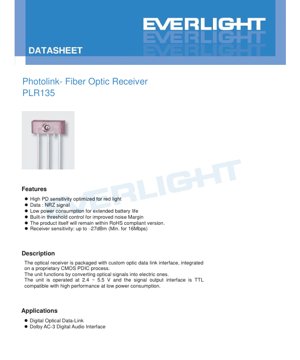
PLR135 एक कॉम्पैक्ट, उच्च-प्रदर्शन ऑप्टिकल फाइबर रिसीवर मॉड्यूल है, जो विशेष रूप से ऑप्टिकल सिग्नल को TTL-संगत विद्युत सिग्नल में परिवर्तित करने के लिए डिज़ाइन किया गया है। यह 650nm चरम संवेदनशीलता तरंगदैर्ध्य वाली लाल रोशनी के लिए अनुकूलित है। यह उपकरण मालिकाना CMOS PDIC (फोटोडिटेक्टर इंटीग्रेटेड सर्किट) प्रक्रिया पर आधारित है, जो प्रदर्शन और कम बिजली खपत के बीच एक अच्छा संतुलन प्रदान करता है, जिससे यह बैटरी से चलने वाले अनुप्रयोगों के लिए उपयुक्त है। इसका मुख्य कार्य एक विश्वसनीय ऑप्टिकल फाइबर डिजिटल डेटा लिंक स्थापित करना है।
1.1 मुख्य लाभ और लक्षित बाजार
PLR135 के प्रमुख लाभ इसके डिज़ाइन अनुकूलन से उत्पन्न होते हैं। इसमें लाल रोशनी (जिसका उपयोग अक्सर प्लास्टिक ऑप्टिकल फाइबर POF प्रणालियों में किया जाता है) के लिए उच्च फोटोडायोड संवेदनशीलता है। अंतर्निहित थ्रेशोल्ड नियंत्रण सर्किट शोर सहनशीलता को बढ़ाता है, जिससे विभिन्न परिस्थितियों में सिग्नल अखंडता में सुधार होता है। इसकी कम बिजली खपत विशेषता उन पोर्टेबल उपकरणों या प्रणालियों के लिए महत्वपूर्ण है जिन्हें लंबी बैटरी लाइफ की आवश्यकता होती है। इस रिसीवर के प्रमुख लक्षित बाजारों में डिजिटल ऑडियो इंटरफेस (जैसे Dolby AC-3 सिस्टम) और औद्योगिक नियंत्रण, उपभोक्ता इलेक्ट्रॉनिक्स और लघु दूरी संचार प्रणालियों के लिए सामान्य डिजिटल ऑप्टिकल फाइबर डेटा लिंक शामिल हैं।
2. तकनीकी मापदंडों का गहन विश्लेषण
यह खंड डेटाशीट के आधार पर, PLR135 के विनिर्देश मापदंडों का विस्तृत, वस्तुनिष्ठ विश्लेषण प्रस्तुत करता है।
2.1 पूर्ण अधिकतम रेटिंग
ये रेटिंग उन तनाव सीमाओं को परिभाषित करती हैं जो डिवाइस को स्थायी क्षति पहुंचा सकती हैं। इस सीमा से बाहर संचालन करने पर डिवाइस के सही कामकाज की गारंटी नहीं दी जा सकती।
- आपूर्ति वोल्टेज (Vcc):-0.5V से +5.5V। इस सीमा से अधिक वोल्टेज लगाने से आंतरिक CMOS सर्किट को क्षति पहुंचने का जोखिम होता है।
- आउटपुट वोल्टेज (Vout):Vcc + 0.3V से अधिक नहीं होना चाहिए। यह आउटपुट ड्राइवर चरण की सुरक्षा के लिए है।
- भंडारण तापमान (Tstg):-40°C से +85°C। इस तापमान सीमा में भंडारित करने पर डिवाइस के प्रदर्शन में गिरावट नहीं आएगी।
- कार्य तापमान (Topr):-20°C से +70°C। इस परिवेश तापमान सीमा में, डिवाइस अपनी विद्युत विशिष्टताओं को पूरा करने की गारंटी देता है।
- सोल्डरिंग तापमान (Tsol):260°C, अधिकतम 10 सेकंड। यह सामान्य लीड-फ्री रीफ्लो सोल्डरिंग प्रक्रिया आवश्यकताओं के अनुरूप है।
- ESD रेटिंग:ह्यूमन बॉडी मॉडल (HBM): 2000V; मशीन मॉडल (MM): 100V। ये मानदंड घटक की स्थिरवैद्युत निर्वहन सहनशीलता को दर्शाते हैं, और संचालन एवं असेंबली प्रक्रियाओं के लिए मार्गदर्शन प्रदान करते हैं।
2.2 अनुशंसित कार्य स्थितियाँ
सामान्य संचालन और ऑप्टोइलेक्ट्रॉनिक विशेषताओं की तालिका में सूचीबद्ध प्रदर्शन प्राप्त करने के लिए, डिवाइस को इन शर्तों के तहत संचालित किया जाना चाहिए।
- आपूर्ति वोल्टेज (Vcc):2.4V (न्यूनतम), 3.0V (विशिष्ट), 5.5V (अधिकतम)। विशिष्ट ऑपरेटिंग बिंदु 3.0V या 3.3V है।
2.3 प्रकाशविद्युत विशेषताएँ
ये पैरामीटर विशिष्ट शर्तों (Ta=25°C, Vcc=3V, CL=5pF) के तहत मापे गए हैं, जो रिसीवर के प्रदर्शन को परिभाषित करते हैं।
- शिखर संवेदनशीलता तरंगदैर्ध्य (λp):650 nm. रिसीवर इस लाल प्रकाश तरंगदैर्ध्य के प्रति सबसे अधिक संवेदनशील है।
- संचरण दूरी (d):0.2 से 5 मीटर। यह मानक प्लास्टिक ऑप्टिकल फाइबर (POF) की विशिष्ट संचरण सीमा है।
- प्रकाश शक्ति सीमा (Pc):न्यूनतम प्राप्त शक्ति (Pc,min): -27 dBm (न्यूनतम); अधिकतम प्राप्त शक्ति (Pc,max): -14 dBm (अधिकतम)। 16 Mbps दर पर सामान्य संचालन के लिए, इनपुट प्रकाश शक्ति -27 dBm से -14 dBm की सीमा के भीतर होनी चाहिए। अधिकतम मान से अधिक होने पर रिसीवर संतृप्त हो जाएगा।
- शक्ति खपत धारा (Icc):4 mA (विशिष्ट), 12 mA (अधिकतम)। यह स्थैतिक धारा सीधे सिस्टम की शक्ति खपत को प्रभावित करती है।
- आउटपुट वोल्टेज स्तर:उच्च-स्तर आउटपुट वोल्टेज (VOH): 2.1V (न्यूनतम), 2.5V (विशिष्ट) @ Vcc=3V। निम्न-स्तर आउटपुट वोल्टेज (VOL): 0.2V (विशिष्ट), 0.4V (अधिकतम)। ये मानक TTL-संगत स्तर हैं।
- गतिशील प्रदर्शन:
- उदगम/अवरोही समय (tr, tf): 10 ns (विशिष्ट), 20 ns (अधिकतम)।
- प्रसार विलंब (tPLH, tPHL): 120 ns (अधिकतम)।
- पल्स चौड़ाई विरूपण (Δtw): ±25 ns (अधिकतम)। यह निम्न से उच्च और उच्च से निम्न विलंब के बीच के अंतर को संदर्भित करता है।
- जिटर (Δtj): इनपुट पावर के साथ परिवर्तनशील। -14 dBm पर: 1 ns (विशिष्ट), 15 ns (अधिकतम)। -27 dBm पर: 5 ns (विशिष्ट), 20 ns (अधिकतम)। जब सिग्नल न्यूनतम संवेदनशीलता के निकट होता है, तो जिटर बढ़ जाता है।
- ट्रांसमिशन रेट (T):NRZ (नॉन-रिटर्न टू जीरो) सिग्नल का समर्थन करता है, रेट रेंज 0.1 से 16 Mbps तक। यह इसकी डेटा रेट क्षमता को परिभाषित करता है।
3. प्रदर्शन वक्र विश्लेषण
डेटाशीट डिजाइन के लिए महत्वपूर्ण टाइपिकल परफॉर्मेंस कर्व प्रदान करती है।
3.1 वोल्टेज और संवेदनशीलता संबंध
चित्र 4 ऑपरेटिंग वोल्टेज और न्यूनतम प्राप्त शक्ति (संवेदनशीलता) के बीच संबंध दर्शाता है। जैसे-जैसे सप्लाई वोल्टेज 2.4V से 5.5V की ओर बढ़ता है, संवेदनशीलता आम तौर पर सुधरती है (dBm मान अधिक नकारात्मक हो जाता है, जिसका अर्थ है कमजोर सिग्नल का पता लगाने की क्षमता)। उदाहरण के लिए, 3.3V पर, 16 Mbps पर संवेदनशीलता लगभग -28 dBm हो सकती है, जबकि 5.0V पर यह -29 dBm तक बेहतर हो सकती है। विशिष्ट संवेदनशीलता आवश्यकताओं के आधार पर ऑपरेटिंग वोल्टेज चुनने के लिए यह कर्व डिजाइनर के लिए महत्वपूर्ण है।
3.2 डेटा दर और संवेदनशीलता संबंध
चित्र 5 डेटा दर और रिसीवर संवेदनशीलता के बीच व्यापार-संबंध को दर्शाता है। डेटा दर बढ़ने के साथ, त्रुटि-मुक्त संचालन प्राप्त करने के लिए आवश्यक न्यूनतम ऑप्टिकल शक्ति भी बढ़ जाती है (संवेदनशीलता खराब हो जाती है, dBm मान का ऋणात्मक परिमाण कम हो जाता है)। 16 Mbps और 3.3V पर, संवेदनशीलता -28 dBm हो सकती है, लेकिन 25 Mbps पर, यह -24 dBm तक गिर सकती है। किसी विशिष्ट डेटा दर पर अधिकतम संभव लिंक लंबाई या आवश्यक ट्रांसमीटर शक्ति निर्धारित करने के लिए यह चित्र महत्वपूर्ण है।
4. यांत्रिक और पैकेजिंग जानकारी
4.1 पैकेज आयाम और पिन परिभाषा
PLR135 एक कॉम्पैक्ट 3-पिन पैकेज में आता है। पिन कार्य स्पष्ट रूप से परिभाषित हैं:
- पिन 1: Vout- TTL आउटपुट सिग्नल।
- पिन 2: GND- ग्राउंड।
- पिन 3: Vcc- पावर सप्लाई वोल्टेज (2.4V - 5.5V)।
आयाम चित्र सटीक भौतिक आयाम, पिन पिच और स्थिति निर्धारित करता है। सामान्य सहनशीलता ±0.10 mm है। सही PCB असेंबली के लिए इस चित्र के आधार पर सटीक पैड डिजाइन आवश्यक है।
5. अनुप्रयोग सर्किट और डिजाइन मार्गदर्शिका
5.1 मानक अनुप्रयोग सर्किट
डेटाशीट दो संदर्भ परिपथ प्रदान करती है: एक 3V आपूर्ति के लिए और दूसरा 5V आपूर्ति के लिए। दोनों परिपथ मूल रूप से समान हैं और दोनों उचित बिजली आपूर्ति डिकपलिंग पर जोर देते हैं।
- एक 0.1 µF सिरेमिक संधारित्र (C1) को PLR135 के Vcc और GND पिनों के यथासंभव निकट, आदर्श रूप से 7mm के भीतर, रखा जाना चाहिए। यह संधारित्र बिजली रेखा पर उच्च-आवृत्ति शोर के लिए एक कम प्रतिबाधा पथ प्रदान करता है, जो कम जिटर प्रदर्शन बनाए रखने के लिए महत्वपूर्ण है।
- बिजली रेखा में श्रृंखला में एक प्रेरक (L2, 47 µH) जोड़ें। यह रिसीवर के बिजली नोड को बोर्ड पर अन्य स्थानों से आने वाले डिजिटल शोर से अलग करने में मदद करता है।
- आउटपुट के लिए, एक छोटा लोड संधारित्र (C2, 30 pF सुझाया गया) इस्तेमाल किया जा सकता है, लेकिन इसके मान को न्यूनतम रखा जाना चाहिए क्योंकि यह राइज/फॉल समय को प्रभावित करता है।
5.2 PCB लेआउट सुझाव
निर्दिष्ट जिटर और कम इनपुट पावर प्रदर्शन प्राप्त करने के लिए, सावधानीपूर्वक PCB लेआउट आवश्यक है:
- डिकपलिंग:0.1 µF डिकपलिंग कैपेसिटर सरफेस माउंट प्रकार (0805 या छोटा) होना चाहिए और डिवाइस Vcc और Gnd पिन के 2 सेमी के दायरे में रखा जाना चाहिए। यह डिकपलिंग पथ में परजीवी इंडक्टेंस को न्यूनतम करता है।
- पावर प्लेन:POF रिसीवर क्षेत्र के नीचे अलग Vcc और GND प्लेन रखने की दृढ़ता से सिफारिश की जाती है। डिवाइस को सीधे इन प्लेन के ऊपर माउंट किया जाना चाहिए। यह प्लेन कैपेसिटेंस बनाता है जो एक उच्च-आवृत्ति फिल्टर के रूप में कार्य करता है, मदरबोर्ड पर अन्य डिजिटल सर्किट से शोर युग्मन को काफी कम करता है।
- सिग्नल आइसोलेशन:संवेदनशील इनपुट पथ (ऑप्टिकल इंटरफेस क्षेत्र) और आउटपुट ट्रेस को शोरग्रस्त डिजिटल लाइनों या स्विचिंग पावर सप्लाई से दूर रखें।
6. पैकेजिंग एवं आर्डर जानकारी
6.1 लेबल विवरण एवं पैकेजिंग
उत्पाद लेबल में ट्रेसबिलिटी और विनिर्देश पहचान के लिए कई कोड शामिल हैं:
- P/N:उत्पाद मॉडल (उदाहरण के लिए, PLR135)।
- CPN:ग्राहक पार्ट नंबर (यदि आवंटित किया गया है)।
- LOT No.:उत्पादन बैच संख्या, जिसका उपयोग पता लगाने के लिए किया जाता है।
- अन्य कोड जैसे CAT, HUE और REF विभिन्न मापदंडों के लिए आंतरिक ग्रेड कोड हैं (सार्वजनिक डेटा शीट में विस्तृत नहीं)।
मानक पैकेजिंग विशिष्टता प्रति बैग 250 टुकड़े, प्रति कार्टन 4 बैग (प्रति कार्टन कुल 1000 टुकड़े) है।
7. अनुप्रयोग नोट्स एवं डिज़ाइन विचार
7.1 विशिष्ट अनुप्रयोग परिदृश्य
- डिजिटल ऑडियो इंटरफ़ेस:Toslink या समान प्लास्टिक ऑप्टिकल फाइबर का उपयोग करके S/PDIF या Dolby Digital (AC-3) सिग्नल संचारित करने वाले उपभोक्ता ऑडियो उपकरणों के लिए उपयुक्त, विद्युत पृथक्करण और शोर प्रतिरोध प्रदान करता है।
- Industrial Data Link:यह फैक्ट्री ऑटोमेशन, कंट्रोल सिस्टम और सेंसर नेटवर्क के लिए उपयोगी है, जहां विद्युत शोर प्रतिरोध, सुरक्षा अलगाव या लघु दूरी पर सुरक्षित डेटा संचरण की आवश्यकता होती है।
- Consumer Electronics:इसका उपयोग सेट-टॉप बॉक्स, गेमिंग कंसोल या हाई-एंड टेलीविजन के आंतरिक या बाहरी डिजिटल ऑडियो कनेक्शन के लिए किया जा सकता है।
7.2 प्रमुख डिज़ाइन विचार
- Optical Power Budget:डिजाइनर को कुल लिंक हानि (फाइबर हानि, कनेक्टर हानि) की गणना करनी चाहिए और यह सुनिश्चित करना चाहिए कि रिसीवर पर प्रकाश शक्ति (Pc) न्यूनतम (-27 dBm) और अधिकतम (-14 dBm) सीमाओं के बीच है। चयनित वोल्टेज और डेटा दर पर प्रदर्शन वक्र (चित्र 4 और चित्र 5) का संदर्भ लेना आवश्यक है।
- Jitter Management:जिटर प्रदर्शन इनपुट पावर और PCB लेआउट पर अत्यधिक निर्भर करता है। न्यूनतम संवेदनशीलता के करीब काम करने से जिटर बढ़ सकता है। उच्च डेटा दर या कम बिजली खपत वाले अनुप्रयोगों के लिए, डिकप्लिंग और लेआउट दिशानिर्देशों का सख्ती से पालन करना आवश्यक है।
- वोल्टेज चयन:हालांकि डिवाइस का कार्यशील वोल्टेज रेंज 2.4V से 5.5V है, लेकिन चयन संवेदनशीलता और बिजली खपत को प्रभावित करता है। उच्च वोल्टेज संवेदनशीलता में सुधार कर सकता है, लेकिन इससे बिजली खपत में मामूली वृद्धि हो सकती है।
8. तकनीकी तुलना एवं विभेदीकरण
हालांकि यह एकल डेटाशीट अन्य मॉडलों के साथ सीधी साइड-बाय-साइड तुलना प्रदान नहीं करती है, लेकिन PLR135 की प्रमुख विभेदक विशेषताओं का अनुमान लगाया जा सकता है:
- 650nm लाल प्रकाश के लिए अनुकूलित:कई सामान्य रिसीवर में व्यापक संवेदनशीलता रेंज होती है, लेकिन 650nm POF सिस्टम के लिए अनुकूलन, ब्रॉडबैंड डिवाइस की तुलना में, उस विशिष्ट तरंगदैर्ध्य पर बेहतर संवेदनशीलता प्राप्त कर सकता है।
- अंतर्निहित सीमा नियंत्रण:यह सुविधा स्वचालित रूप से निर्णय सीमा को समायोजित करती है, जो विभिन्न स्थितियों (जैसे तापमान परिवर्तन या ट्रांसमीटर के पुराने होने) के तहत शोर सहनशीलता में सुधार करती है। सभी बुनियादी रिसीवर में यह सुविधा शामिल नहीं होती है, जो PLR135 को और अधिक मजबूत बनाती है।
- CMOS PDIC प्रक्रिया:CMOS प्लेटफॉर्म पर एकीकरण, पुराने द्विध्रुवी या अलग-अलग डिजाइनों की तुलना में, आमतौर पर कम बिजली की खपत और आधुनिक डिजिटल सिस्टम के साथ बेहतर संगतता प्राप्त करने में सक्षम बनाता है।
9. सामान्य प्रश्न (FAQ)
Q1: PLR135 की अधिकतम डेटा दर क्या है?
A1: डेटाशीट के अनुसार, PLR135 0.1 Mbps से 16 Mbps तक की NRZ डेटा दरों का समर्थन करता है। इससे अधिक गति पर चलाने का प्रयास बिट त्रुटि दर में वृद्धि का कारण बन सकता है।
Q2: क्या मैं इस रिसीवर का उपयोग इन्फ्रारेड (850nm या 1300nm) ऑप्टिकल फाइबर केबल के साथ कर सकता हूं?
A2: नहीं। यह डिवाइस विशेष रूप से 650nm (लाल प्रकाश) के पीक संवेदनशीलता के लिए अनुकूलित है। इन्फ्रारेड तरंगदैर्ध्य पर इसकी संवेदनशीलता काफी कम हो जाएगी, जिससे यह मानक इन्फ्रारेड-आधारित ऑप्टिकल फाइबर सिस्टम के लिए अनुपयुक्त होने की संभावना है।
Q3: मेरी इनपुट ऑप्टिकल पावर -30 dBm है। क्या PLR135 काम करेगा?
A3: नहीं। निर्दिष्ट न्यूनतम प्राप्त शक्ति -27 dBm है। -30 dBm का सिग्नल संवेदनशीलता सीमा से नीचे है, और रिसीवर इसे विश्वसनीय रूप से पहचान नहीं पाएगा। आपको एक अधिक संवेदनशील रिसीवर, एक उच्च शक्ति वाला ट्रांसमीटर, या कम हानि वाला ऑप्टिकल फाइबर लिंक चाहिए।
Q4: 0.1 µF डिकप्लिंग कैपेसिटर के प्लेसमेंट का कितना महत्व है?
A4: अत्यंत महत्वपूर्ण। खराब डिकप्लिंग हाई-स्पीड रिसीवर सर्किट में अत्यधिक जिटर और अस्थिर संचालन का सबसे आम कारण है। इसे 2 सेमी के भीतर (आदर्श रूप से और करीब) रखना एक कठिन आवश्यकता है, सुझाव नहीं।
Q5: "NRZ सिग्नल" का क्या अर्थ है?
A5: NRZ का मतलब नॉन-रिटर्न टू जीरो है। यह एक सामान्य डिजिटल एन्कोडिंग योजना है जिसमें उच्च सिग्नल स्तर (जैसे, प्रकाश चालू) लॉजिकल '1' का प्रतिनिधित्व करता है और निम्न स्तर (प्रकाश बंद) लॉजिकल '0' का प्रतिनिधित्व करता है। सिग्नल बिट्स के बीच तटस्थ अवस्था में वापस नहीं लौटता है।
10. कार्य सिद्धांत का संक्षिप्त परिचय
PLR135 मूल प्रकाशविद्युत सिद्धांत पर कार्य करता है। 650nm ऑप्टिकल फाइबर से प्रकाश को CMOS चिप पर एकीकृत फोटोडायोड (PD) पर केंद्रित किया जाता है। फोटोडायोड आपतित फोटॉनों को आनुपातिक फोटोकरंट में परिवर्तित करता है। इस सूक्ष्म धारा को फिर एक उच्च लाभ, कम शोर ट्रांसइम्पीडेंस एम्पलीफायर (TIA) में भेजा जाता है, जो इसे वोल्टेज सिग्नल में बदल देता है। TIA के बाद, एक लिमिटिंग एम्पलीफायर सिग्नल को एक समान डिजिटल स्तर तक बढ़ा देता है। अंतर्निहित थ्रेशोल्ड नियंत्रण सर्किट बेसलाइन ड्रिफ्ट और निम्न-आवृत्ति शोर के लिए क्षतिपूर्ति करने के लिए डिजिटल लिमिटर के निर्णय बिंदु को गतिशील रूप से समायोजित करता है, जिससे बिट एरर रेट में सुधार होता है। अंत में, एक आउटपुट बफर स्टेज मूल ऑप्टिकल इनपुट के अनुरूप एक स्वच्छ, TTL-संगत डिजिटल सिग्नल प्रदान करता है।
11. उद्योग रुझान और पृष्ठभूमि
PLR135 जैसे उपकरण ऑप्टिकल फाइबर घटक बाजार में एक परिपक्व और अनुकूलित क्षेत्र का प्रतिनिधित्व करते हैं। इस प्रकार के उपभोक्ता-ग्रेड और औद्योगिक-ग्रेड लघु दूरी के ऑप्टिकल लिंक के रुझान हैं:
- उच्च एकीकरण:रिसीवर फोटोडायोड, एम्पलीफायर और डिजिटल लॉजिक को एक एकल CMOS चिप में एकीकृत करना (जैसा कि यहां देखा गया है), आकार, लागत और बिजली की खपत को कम करता है।
- कम बिजली की खपत:पोर्टेबल और बैटरी से चलने वाले उपकरणों के प्रचलन से प्रेरित होकर, नई पीढ़ी के उपकरण लगातार कम ऑपरेटिंग करंट की मांग कर रहे हैं।
- उच्च डेटा दर:हालांकि ऑडियो और कई नियंत्रण अनुप्रयोगों के लिए 16 Mbps पर्याप्त है, लेकिन वीडियो और तेज डेटा ट्रांसमिशन की मांग POF के माध्यम से 100 Mbps और उससे अधिक की दर प्राप्त करने में सक्षम रिसीवर के विकास को प्रेरित कर रही है।
- अधिक मजबूती:वास्तविक शोरगुल वाले वातावरण में विश्वसनीयता बढ़ाने के लिए, स्वचालित थ्रेशोल्ड नियंत्रण और उच्च ESD सुरक्षा जैसी सुविधाएं अब मानक बनती जा रही हैं।
PLR135 उन अनुप्रयोग परिदृश्यों के लिए उपयुक्त है जहां विश्वसनीयता, शोर प्रतिरोध और विद्युत पृथक्करण अत्यधिक उच्च डेटा दर या ट्रांसमिशन दूरी से अधिक महत्वपूर्ण हैं, जो कांच ऑप्टिकल फाइबर और लेजर-आधारित प्रणालियों का क्षेत्र है।
LED विनिर्देश शब्दावली का विस्तृत विवरण
LED तकनीकी शब्दावली की संपूर्ण व्याख्या
1. प्रकाश-विद्युत प्रदर्शन के मुख्य संकेतक
| शब्दावली | इकाई/प्रतिनिधित्व | सामान्य व्याख्या | यह महत्वपूर्ण क्यों है |
|---|---|---|---|
| दीप्त प्रभावकारिता (Luminous Efficacy) | lm/W (लुमेन प्रति वाट) | प्रति वाट विद्युत ऊर्जा से उत्सर्जित प्रकाश प्रवाह, जितना अधिक होगा उतनी अधिक ऊर्जा बचत। | सीधे तौर पर प्रकाश उपकरण की ऊर्जा दक्षता श्रेणी और बिजली लागत निर्धारित करता है। |
| प्रकाश प्रवाह (Luminous Flux) | lm (लुमेन) | प्रकाश स्रोत द्वारा उत्सर्जित कुल प्रकाश मात्रा, जिसे आम बोलचाल में "चमक" कहा जाता है। | यह निर्धारित करता है कि प्रकाश जुड़नार पर्याप्त रूप से चमकीला है या नहीं। |
| प्रकाश उत्सर्जन कोण (Viewing Angle) | ° (डिग्री), जैसे 120° | वह कोण जिस पर प्रकाश तीव्रता आधी रह जाती है, यह प्रकाश पुंज की चौड़ाई निर्धारित करता है। | यह प्रकाश के कवरेज क्षेत्र और एकरूपता को प्रभावित करता है। |
| वर्ण तापमान (CCT) | K (केल्विन), जैसे 2700K/6500K | प्रकाश का रंग गर्म या ठंडा, कम मान पीला/गर्म, उच्च मान सफेद/ठंडा। | प्रकाश व्यवस्था के वातावरण और उपयुक्त परिदृश्यों को निर्धारित करता है। |
| रंग प्रतिपादन सूचकांक (CRI / Ra) | कोई इकाई नहीं, 0–100 | प्रकाश स्रोत द्वारा वस्तुओं के वास्तविक रंगों को प्रदर्शित करने की क्षमता, Ra≥80 उत्तम माना जाता है। | रंग सटीकता को प्रभावित करता है, शॉपिंग मॉल, आर्ट गैलरी जैसे उच्च आवश्यकता वाले स्थानों के लिए उपयोग किया जाता है। |
| रंग सहनशीलता (SDCM) | मैकएडम एलिप्स चरण, जैसे "5-step" | रंग एकरूपता का मात्रात्मक माप, चरण संख्या जितनी कम होगी, रंग उतने ही अधिक सुसंगत होंगे। | यह सुनिश्चित करता है कि एक ही बैच के दीपकों के रंगों में कोई अंतर न हो। |
| प्रमुख तरंगदैर्ध्य (Dominant Wavelength) | nm (नैनोमीटर), उदाहरणार्थ 620nm (लाल) | रंगीन LED रंगों के संगत तरंगदैर्ध्य मान। | लाल, पीला, हरा आदि एकवर्णी LED के रंगतत्व (ह्यू) को निर्धारित करता है। |
| स्पेक्ट्रम वितरण (Spectral Distribution) | तरंगदैर्ध्य बनाम तीव्रता वक्र | LED द्वारा उत्सर्जित प्रकाश की विभिन्न तरंगदैर्ध्य पर तीव्रता वितरण को प्रदर्शित करता है। | रंग प्रतिपादन और रंग गुणवत्ता को प्रभावित करता है। |
दो, विद्युत मापदंड
| शब्दावली | प्रतीक | सामान्य व्याख्या | डिज़ाइन संबंधी विचार |
|---|---|---|---|
| फॉरवर्ड वोल्टेज (Forward Voltage) | Vf | LED को प्रकाशित करने के लिए आवश्यक न्यूनतम वोल्टेज, "स्टार्ट-अप थ्रेशोल्ड" के समान। | ड्राइविंग पावर सप्लाई वोल्टेज ≥ Vf होना चाहिए, कई LEDs को श्रृंखला में जोड़ने पर वोल्टेज जुड़ जाता है। |
| फॉरवर्ड करंट (Forward Current) | If | LED को सामान्य रूप से प्रकाशित करने वाला करंट मान। | आमतौर पर कॉन्स्टेंट करंट ड्राइव का उपयोग किया जाता है, करंट चमक और आयु निर्धारित करता है। |
| अधिकतम स्पंद धारा (Pulse Current) | Ifp | अल्प अवधि के लिए सहन योग्य शिखर धारा, डिमिंग या फ्लैश के लिए उपयोग की जाती है। | स्पंद चौड़ाई और ड्यूटी साइकिल को सख्ती से नियंत्रित किया जाना चाहिए, अन्यथा अत्यधिक गर्मी से क्षति होगी। |
| विपरीत वोल्टेज (Reverse Voltage) | Vr | LED सहन कर सकने वाला अधिकतम रिवर्स वोल्टेज, जिससे अधिक होने पर ब्रेकडाउन हो सकता है। | सर्किट में रिवर्स कनेक्शन या वोल्टेज स्पाइक से बचाव आवश्यक है। |
| Thermal Resistance | Rth (°C/W) | चिप से सोल्डर पॉइंट तक ऊष्मा प्रवाह का प्रतिरोध, कम मान बेहतर हीट डिसिपेशन दर्शाता है। | उच्च थर्मल रेजिस्टेंस के लिए मजबूत हीट सिंक डिज़ाइन की आवश्यकता होती है, अन्यथा जंक्शन तापमान बढ़ जाता है। |
| इलेक्ट्रोस्टैटिक डिस्चार्ज इम्यूनिटी (ESD Immunity) | V (HBM), जैसे 1000V | इलेक्ट्रोस्टैटिक शॉक प्रतिरोध क्षमता, मान जितना अधिक होगा, स्थैतिक बिजली से क्षतिग्रस्त होने की संभावना उतनी ही कम होगी। | उत्पादन में इलेक्ट्रोस्टैटिक डिस्चार्ज सुरक्षा उपाय करने आवश्यक हैं, विशेष रूप से उच्च संवेदनशीलता वाले LED के लिए। |
तीन, ताप प्रबंधन और विश्वसनीयता
| शब्दावली | प्रमुख संकेतक | सामान्य व्याख्या | प्रभाव |
|---|---|---|---|
| जंक्शन तापमान (Junction Temperature) | Tj (°C) | LED चिप का आंतरिक वास्तविक कार्य तापमान। | प्रत्येक 10°C कमी पर, जीवनकाल दोगुना हो सकता है; अत्यधिक तापमान से लुमेन ह्रास और रंग विस्थापन होता है। |
| लुमेन ह्रास (Lumen Depreciation) | L70 / L80 (घंटे) | चमक प्रारंभिक मान के 70% या 80% तक गिरने में लगने वाला समय। | LED के "उपयोगी जीवन" को सीधे परिभाषित करता है। |
| लुमेन रखरखाव दर (Lumen Maintenance) | % (जैसे 70%) | एक निश्चित उपयोग अवधि के बाद शेष चमक का प्रतिशत। | दीर्घकालिक उपयोग के बाद चमत्कार बनाए रखने की क्षमता को दर्शाता है। |
| रंग परिवर्तन (Color Shift) | Δu′v′ या मैकएडम दीर्घवृत्त | उपयोग के दौरान रंग में परिवर्तन की मात्रा। | प्रकाश व्यवस्था के दृश्य की रंग एकरूपता को प्रभावित करता है। |
| तापीय वृद्धि (Thermal Aging) | सामग्री प्रदर्शन में गिरावट | लंबे समय तक उच्च तापमान के कारण एनकैप्सुलेशन सामग्री का क्षरण। | चमक में कमी, रंग परिवर्तन या ओपन-सर्किट विफलता का कारण बन सकता है। |
चार, पैकेजिंग और सामग्री
| शब्दावली | सामान्य प्रकार | सामान्य व्याख्या | विशेषताएं और अनुप्रयोग |
|---|---|---|---|
| एनकैप्सुलेशन प्रकार | EMC, PPA, सिरेमिक | चिप की सुरक्षा करने और प्रकाशिकी एवं ऊष्मा अंतरापृष्ठ प्रदान करने वाली आवरण सामग्री। | EMC उच्च तापसहिष्णुता, कम लागत; सिरेमिक बेहतर ताप अपव्यय, लंबी आयु। |
| चिप संरचना | फॉरवर्ड माउंट, फ्लिप चिप | चिप इलेक्ट्रोड व्यवस्था का तरीका। | उलटी स्थापना में बेहतर ताप निकासी और उच्च प्रकाश दक्षता होती है, जो उच्च शक्ति के लिए उपयुक्त है। |
| फॉस्फर कोटिंग | YAG, सिलिकेट, नाइट्राइड | नीले प्रकाश चिप पर लगाया जाता है, जो कुछ हिस्से को पीले/लाल प्रकाश में बदल देता है और सफेद प्रकाश में मिला देता है। | विभिन्न फॉस्फर प्रकाश दक्षता, रंग तापमान और रंग प्रतिपादन को प्रभावित करते हैं। |
| लेंस/ऑप्टिकल डिज़ाइन | समतल, माइक्रोलेंस, कुल आंतरिक परावर्तन | एनकैप्सुलेशन सतह की प्रकाशिक संरचना, प्रकाश वितरण को नियंत्रित करती है। | उत्सर्जन कोण और प्रकाश वितरण वक्र निर्धारित करता है। |
पाँच, गुणवत्ता नियंत्रण और ग्रेडिंग
| शब्दावली | ग्रेडिंग विषयवस्तु | सामान्य व्याख्या | उद्देश्य |
|---|---|---|---|
| ल्यूमिनस फ्लक्स बिनिंग | कोड जैसे 2G, 2H | चमक के स्तर के अनुसार समूहीकरण, प्रत्येक समूह का न्यूनतम/अधिकतम लुमेन मान होता है। | यह सुनिश्चित करना कि एक ही बैच के उत्पादों की चमक समान हो। |
| वोल्टेज बिनिंग | कोड जैसे 6W, 6X | फॉरवर्ड वोल्टेज रेंज के अनुसार समूहीकरण। | ड्राइव पावर मिलान की सुविधा, सिस्टम दक्षता में सुधार। |
| रंग ग्रेडिंग | 5-step MacAdam ellipse | रंग निर्देशांक के अनुसार समूहीकरण, यह सुनिश्चित करते हुए कि रंग बहुत छोटी सीमा के भीतर आता है। | रंग एकरूपता सुनिश्चित करें, एक ही लैंप के भीतर रंग असमानता से बचें। |
| रंग तापमान श्रेणीकरण | 2700K, 3000K, आदि। | रंग तापमान के अनुसार समूहीकरण करें, प्रत्येक समूह की अपनी संबंधित निर्देशांक सीमा होती है। | विभिन्न परिदृश्यों की रंग तापमान आवश्यकताओं को पूरा करें। |
छह, परीक्षण और प्रमाणन
| शब्दावली | मानक/परीक्षण | सामान्य व्याख्या | महत्व |
|---|---|---|---|
| LM-80 | लुमेन रखरखाव परीक्षण | निरंतर तापमान की स्थिति में लंबे समय तक जलाकर, चमक क्षय डेटा रिकॉर्ड करना। | एलईडी जीवनकाल का अनुमान लगाने के लिए (TM-21 के साथ संयोजन में)। |
| TM-21 | जीवनकाल प्रक्षेपण मानक | LM-80 डेटा के आधार पर वास्तविक उपयोग की स्थितियों में जीवनकाल का अनुमान लगाना। | वैज्ञानिक जीवनकाल पूर्वानुमान प्रदान करना। |
| IESNA मानक | इल्युमिनेटिंग इंजीनियरिंग सोसाइटी मानक | ऑप्टिकल, इलेक्ट्रिकल और थर्मल परीक्षण विधियों को शामिल करता है। | उद्योग द्वारा स्वीकृत परीक्षण आधार। |
| RoHS / REACH | पर्यावरण प्रमाणन | यह सुनिश्चित करता है कि उत्पाद में हानिकारक पदार्थ (जैसे सीसा, पारा) न हों। | अंतरराष्ट्रीय बाजार में प्रवेश के लिए पात्रता शर्त। |
| ENERGY STAR / DLC | ऊर्जा दक्षता प्रमाणन | प्रकाश उत्पादों के लिए ऊर्जा दक्षता और प्रदर्शन प्रमाणन। | आमतौर पर सरकारी खरीद, सब्सिडी कार्यक्रमों में उपयोग किया जाता है, बाजार प्रतिस्पर्धा बढ़ाने के लिए। |