विषय सूची
- 1. उत्पाद अवलोकन
- 2. तकनीकी मापदंड गहन उद्देश्य व्याख्या
- 2.1 पूर्ण अधिकतम रेटिंग्स
- 2.2 विद्युत और स्थानांतरण विशेषताएँ
- 3. स्विचिंग विशेषताएँ
- 4. Mechanical and Package Information
- 4.1 Pin Configuration
- 5. एप्लिकेशन सुझाव
- 5.1 विशिष्ट एप्लिकेशन परिदृश्य
- 5.2 Design Considerations
- 6. तकनीकी तुलना और चयन मार्गदर्शिका
- 7. अक्सर पूछे जाने वाले प्रश्न (तकनीकी मापदंडों के आधार पर)
- 8. Principle Introduction
- 9. Packaging and Ordering Information
1. उत्पाद अवलोकन
6N135, 6N136, EL4502, और EL4503 हाई-स्पीड ट्रांजिस्टर आउटपुट फोटोकपलर (ऑप्टोआइसोलेटर) का एक परिवार है, जो तेज डिजिटल सिग्नल अलगाव की आवश्यकता वाले अनुप्रयोगों के लिए डिज़ाइन किया गया है। प्रत्येक डिवाइस एक इन्फ्रारेड लाइट-एमिटिंग डायोड (LED) को एक हाई-स्पीड फोटोडिटेक्टर ट्रांजिस्टर से ऑप्टिकली युग्मित करता है। इस श्रृंखला का मुख्य लाभ इसके समर्पित पिनआउट में निहित है, जो फोटोडायोड बायस और आउटपुट ट्रांजिस्टर के कलेक्टर को अलग करता है। यह आर्किटेक्चरल विकल्प इनपुट ट्रांजिस्टर की बेस-कलेक्टर कैपेसिटेंस को काफी कम कर देता है, जिससे स्विचिंग स्पीड 1 मेगाबिट प्रति सेकंड (1Mbit/s) तक पहुंच जाती है, जो पारंपरिक फोटोट्रांजिस्टर-आधारित कपलर की तुलना में कई गुना तेज है।
ये डिवाइस एक मानक 8-पिन ड्यूल इन-लाइन पैकेज (DIP) में उपलब्ध हैं और इन्हें वाइड लीड स्पेसिंग और सरफेस-माउंट कॉन्फ़िगरेशन विकल्पों के साथ भी प्राप्त किया जा सकता है। ये एक विस्तृत तापमान सीमा पर संचालन के लिए चरित्रित हैं और प्रमुख अंतरराष्ट्रीय सुरक्षा मानकों का अनुपालन करते हैं, जिससे ये औद्योगिक, दूरसंचार और पावर इलेक्ट्रॉनिक्स अनुप्रयोगों के लिए उपयुक्त हैं।
2. तकनीकी मापदंड गहन उद्देश्य व्याख्या
2.1 पूर्ण अधिकतम रेटिंग्स
Absolute Maximum Ratings उन तनाव सीमाओं को परिभाषित करते हैं जिनके परे डिवाइस को स्थायी क्षति हो सकती है। इन सीमाओं पर या उनके निकट डिवाइस को लगातार संचालित करने की अनुशंसा नहीं की जाती है। प्रमुख रेटिंग्स में शामिल हैं:
- Input Forward Current (IF)25 mA निरंतर। शिखर अग्र धारा (IFP) को 50% ड्यूटी साइकिल और 1ms पल्स चौड़ाई वाले पल्स के लिए 50 mA पर रेट किया गया है।
- रिवर्स वोल्टेज (VR)इनपुट एलईडी पर अधिकतम 5 V.
- आउटपुट वोल्टेज (VO)आउटपुट पिन पर -0.5 V से +20 V तक की सीमा.
- सप्लाई वोल्टेज (VCC): आउटपुट साइड पावर सप्लाई के लिए -0.5 V से +30 V तक की रेंज।
- इंसुलेशन वोल्टेज (VISO): 5000 Vrms 1 मिनट के लिए। यह एक महत्वपूर्ण सुरक्षा पैरामीटर है, जिसका परीक्षण इनपुट-साइड पिन (1-4) को एक साथ और आउटपुट-साइड पिन (5-8) को एक साथ शॉर्ट करके किया जाता है।
- Operating Temperature (TOPR): -55°C से +100°C तक। यह विस्तृत सीमा कठोर वातावरण में विश्वसनीय प्रदर्शन सुनिश्चित करती है।
- Total Power Dissipation (PTOT): 200 mW, इनपुट और आउटपुट पावर सीमाओं को संयोजित करते हुए।
2.2 विद्युत और स्थानांतरण विशेषताएँ
जब तक अन्यथा नोट न किया गया हो, ये पैरामीटर 0°C से 70°C के ऑपरेटिंग तापमान रेंज पर गारंटीकृत हैं। ये सामान्य ऑपरेटिंग परिस्थितियों में डिवाइस के प्रदर्शन को परिभाषित करते हैं।
- फॉरवर्ड वोल्टेज (VF): आमतौर पर IF = 16 mA पर 1.45V। इनपुट-साइड करंट लिमिटिंग सर्किट डिजाइन करने के लिए यह महत्वपूर्ण है।
- करंट ट्रांसफर रेशियो (CTR): यह आउटपुट ट्रांजिस्टर के कलेक्टर करंट और इनपुट LED के फॉरवर्ड करंट का अनुपात है, जिसे प्रतिशत में व्यक्त किया जाता है। 6N135 का न्यूनतम CTR 7% (सामान्य परिदृश्य) है, जबकि 6N136, EL4502, और EL4503 का न्यूनतम 19% है। यह पैरामीटर किसी दिए गए आउटपुट करंट के लिए आवश्यक ड्राइव करंट को सीधे प्रभावित करता है।
- Logic Low Output Voltage (VOL)डिवाइस के "ON" स्थिति में होने पर आउटपुट पिन पर वोल्टेज। 6N135 के लिए, यह IF=16mA और IO=1.1mA पर 0.4V (अधिकतम) से नीचे होने की गारंटी है। 6N136/EL450x के लिए, यह IO=3mA पर 0.4V से नीचे है। कम VOL स्वच्छ लॉजिक-लो सिग्नल के लिए महत्वपूर्ण है।
- सप्लाई करंट्स (ICCL, ICCH): ICCL is the current drawn from VCC जब आउटपुट कम होता है (LED चालू), आमतौर पर 140 µA। ICCH वह धारा है जब आउटपुट उच्च होता है (LED बंद), आमतौर पर 0.01 µA, जो निष्क्रिय अवस्था में बहुत कम बिजली खपत को दर्शाता है।
3. स्विचिंग विशेषताएँ
ये पैरामीटर डिवाइस की गति को मापते हैं, जो इसका प्राथमिक अंतरकारक है। परीक्षण IF=16mA और VCC=5V पर किए जाते हैं।
- Propagation Delay (tPHL, tPLH): यह इनपुट सिग्नल के किनारे और संबंधित आउटपुट प्रतिक्रिया के बीच का समय विलंब है।
- 6N135: tPHL (निम्न स्तर तक) आमतौर पर 0.35 µs (अधिकतम 2.0 µs) होता है; tPLH (उच्च स्तर तक) आमतौर पर R के साथ 0.5 µs (अधिकतम 2.0 µs) होता हैL=4.1kΩ.
- 6N136/EL450x: tPHL आम तौर पर 0.35 µs (अधिकतम 1.0 µs) होता है; tPLH आम तौर पर 0.3 µs (अधिकतम 1.0 µs) होता है, जब RL=1.9kΩ.
- कॉमन मोड ट्रांजिएंट इम्यूनिटी (CMH, CML): यह आइसोलेशन बैरियर के इनपुट और आउटपुट दोनों पक्षों पर समान रूप से दिखाई देने वाले तीव्र वोल्टेज ट्रांजिएंट (शोर) को अस्वीकार करने की डिवाइस की क्षमता को मापता है। इसे वोल्ट प्रति माइक्रोसेकंड (V/µs) में निर्दिष्ट किया जाता है।
- 6N135/6N136/EL4502: उच्च और निम्न दोनों अवस्थाओं के लिए न्यूनतम 1000 V/µs।
- EL4503: काफी अधिक, जिसका सामान्य मान 20,000 V/µs और न्यूनतम 15,000 V/µs है, जो इसे मोटर ड्राइव जैसे बहुत अधिक शोर वाले वातावरण के लिए आदर्श बनाता है।
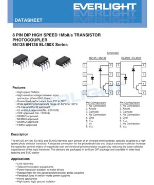
4. Mechanical and Package Information
4.1 Pin Configuration
The devices use an 8-pin DIP package. The pinout differs slightly between the 6N135/6N136 and the EL4502/EL4503, primarily in the function of pin 7.
6N135 / 6N136 के लिए:
- No Connection (NC)
- Anode (Input LED Anode)
- Cathode (Input LED Cathode)
- No Connection (NC)
- ग्राउंड (आउटपुट साइड ग्राउंड, GND)
- आउटपुट वोल्टेज (VOUT)
- Bias Voltage (VB) - यह पिन आंतरिक फोटोडायोड को बायस करने के लिए एक अलग कनेक्शन प्रदान करता है, जो उच्च गति प्राप्त करने के लिए महत्वपूर्ण है।
- सप्लाई वोल्टेज (VCC)
For EL4502 / EL4503:
- No Connection (NC)
- Anode (Input LED Anode)
- Cathode (Input LED Cathode)
- No Connection (NC)
- ग्राउंड (आउटपुट साइड ग्राउंड, GND)
- आउटपुट वोल्टेज (VOUT)
- No Connection (NC) - नोट: इन वेरिएंट में पिन 7 कनेक्ट नहीं है।
- सप्लाई वोल्टेज (VCC)
5. एप्लिकेशन सुझाव
5.1 विशिष्ट एप्लिकेशन परिदृश्य
- Line Receivers & Telecommunications Equipment: डिजिटल डेटा लाइनों को अलग करना (जैसे, RS-232, RS-485) ताकि ग्राउंड लूप को रोका जा सके और संवेदनशील सर्किटरी को सर्ज से बचाया जा सके।
- Power Transistor Isolation in Motor Drives & Switch-Mode Power Supplies (SMPS): गैल्वेनिक आइसोलेशन बनाए रखते हुए हाई-साइड पावर MOSFET/IGBT को गेट ड्राइव सिग्नल प्रदान करना। यहाँ उच्च कॉमन-मोड ट्रांजिएंट इम्यूनिटी (विशेष रूप से EL4503 की) महत्वपूर्ण है।
- हाई-स्पीड लॉजिक ग्राउंड आइसोलेशन: विभिन्न विभवों पर संचालित होने वाले डिजिटल उपतंत्रों के बीच ग्राउंड लूप्स को तोड़ना, शोर युग्मन को रोकना।
- लो-स्पीड फोटोट्रांजिस्टर कपलर्स के लिए प्रतिस्थापन: प्रमुख सर्किट परिवर्तनों के बिना उच्च डेटा दरों के लिए मौजूदा डिजाइनों को उन्नत करना।
- होम Appliances & Industrial Controls: पावर स्टेज से यूजर इंटरफ़ेस माइक्रोकंट्रोलर को अलग करना।
5.2 Design Considerations
- इनपुट करंट लिमिटिंगAn external resistor must be used in series with the input LED to limit the forward current (IF) to the desired value, typically around 16 mA for optimal speed and CTR. The resistor value is calculated as (Supply Voltage - VF) / मैंF.
- आउटपुट पुल-अप रेसिस्टर: एक पुल-अप रेसिस्टर (RL) VOUT (पिन 6) और VCC (पिन 8) के बीच आवश्यक है। इसका मान स्विचिंग गति और आउटपुट करंट क्षमता दोनों को प्रभावित करता है। डेटाशीट RL6N135 के लिए =4.1kΩ और 6N136/EL450x के लिए 1.9kΩ। कम मान गति बढ़ाते हैं लेकिन शक्ति क्षय भी बढ़ाते हैं।
- बाईपास कैपेसिटरVCC और आउटपुट साइड पर GND पिन्स को हाई-फ्रीक्वेंसी नॉइज़ को डिकपल करने के लिए।
- उच्च CMR के लिए लेआउट: उच्च कॉमन-मोड रिजेक्शन बनाए रखने के लिए, सर्किट बोर्ड लेआउट के इनपुट और आउटपुट पक्षों के बीच परजीवी धारिता को न्यूनतम रखें। अलगाव बैरियर के दोनों ओर के ट्रेसों को अच्छी तरह से अलग रखें।
6. तकनीकी तुलना और चयन मार्गदर्शिका
इस श्रृंखला के भीतर प्राथमिक अंतर करंट ट्रांसफर रेशियो (CTR) और कॉमन मोड रिजेक्शन (CMR) में हैं।
- 6N135 बनाम 6N136/EL4502: 6N135 में न्यूनतम CTR कम है (7% बनाम 19%)। इसका अर्थ है कि समान आउटपुट करंट स्विंग प्राप्त करने के लिए इसे थोड़ा अधिक इनपुट करंट की आवश्यकता हो सकती है। 6N136/EL4502 बेहतर मार्जिन प्रदान करता है।
- EL4503 बनाम अन्य: EL4503 अपनी असाधारण रूप से उच्च कॉमन-मोड ट्रांजिएंट इम्यूनिटी (15,000 V/µs न्यूनतम) के साथ अलग दिखता है। यह इसे अत्यधिक उच्च विद्युत शोर वाले अनुप्रयोगों, जैसे कि वेरिएबल फ्रीक्वेंसी ड्राइव्स (VFDs) या औद्योगिक मोटर नियंत्रकों, जहाँ तेज वोल्टेज स्पाइक्स (dV/dt) आम हैं, के लिए पसंदीदा विकल्प बनाता है।
- चयन सारांश:
- सामान्य उद्देश्य वाली उच्च गति वाली अलगाव के लिए अच्छे CTR के साथ: 6N136 या EL4502 चुनें।
- यदि लागत एक प्रमुख कारक है और कम CTR स्वीकार्य है: 6N135 पर्याप्त हो सकता है।
- सबसे चुनौतीपूर्ण, उच्च शोर वाले पावर इलेक्ट्रॉनिक्स वातावरण के लिए: EL4503 विशेष रूप से इस भूमिका के लिए डिज़ाइन किया गया है।
7. अक्सर पूछे जाने वाले प्रश्न (तकनीकी मापदंडों के आधार पर)
Q: What is the main advantage of this photocoupler over a standard 4N35?
A: गति। समर्पित बायस पिन (VB on 6N135/136) आर्किटेक्चर आंतरिक कैपेसिटेंस को कम करता है, जिससे 1Mbit/s पर संचालन संभव होता है, जबकि 4N35 जैसे एक मानक फोटोट्रांजिस्टर कपलर आमतौर पर 100 kbit/s से नीचे सीमित होता है।
Q: क्या मैं इनपुट और आउटपुट दोनों पक्षों के लिए एक ही 5V आपूर्ति का उपयोग कर सकता हूं?
A: विद्युत रूप से, हां, लेकिन इससे अलगाव का उद्देश्य विफल हो जाता है। वास्तविक अलगाव के लिए, इनपुट पक्ष (LED) और आउटपुट पक्ष (डिटेक्टर, VCCGND) को अलग, गैर-जुड़े हुए बिजली आपूर्ति स्रोतों या एक पृथक DC-DC कनवर्टर से संचालित किया जाना चाहिए।
Q: अनुशंसित पुल-अप रोकनेवाला मानों (4.1kΩ बनाम 1.9kΩ) के दो अलग-अलग सेट क्यों हैं?
A: उपकरणों के विभिन्न CTR विनिर्देश अलग-अलग इष्टतम कार्य बिंदुओं की ओर ले जाते हैं। कम CTR वाला 6N135, एक दिए गए आउटपुट लो वोल्टेज विनिर्देश के लिए आउटपुट धारा को सीमित करने के लिए एक उच्च पुल-अप रोकनेवाला का उपयोग करता है, जबकि लक्षित गति को अभी भी प्राप्त करता है। उच्च CTR वाला 6N136/EL450x, एक कम रोकनेवाला मान का उपयोग कर सकता है, जो स्विचिंग गति को और बेहतर बना सकता है।
Q: मेरी असेंबली प्रक्रिया के लिए "Pb free and RoHS compliant" का क्या अर्थ है?
A: इसका अर्थ है कि डिवाइस लीड (Pb) के बिना निर्मित है और Restriction of Hazardous Substances निर्देश का अनुपालन करता है। यह इसे उन क्षेत्रों में बेचे जाने वाले उत्पादों में उपयोग करने की अनुमति देता है जहाँ ये पर्यावरणीय नियम लागू हैं। सोल्डरिंग तापमान रेटिंग (260°C for 10 seconds) लीड-मुक्त सोल्डर प्रक्रियाओं के लिए निर्दिष्ट है।
8. Principle Introduction
A transistor output photocoupler operates on the principle of optical isolation. An electrical current applied to the input side causes an infrared Light Emitting Diode (LED) to emit light. This light travels across a small gap within the package and strikes the base region of a phototransistor on the output side. The incoming photons generate electron-hole pairs in the base, effectively acting as a base current. This "optical base current" turns the transistor on, allowing a much larger collector current to flow from VCC आउटपुट पिन से, ट्रांजिस्टर के माध्यम से लो पुल किया गया। जब इनपुट करंट शून्य होता है, तो एलईडी बंद रहती है, कोई प्रकाश ट्रांजिस्टर पर नहीं पड़ता, और यह ऑफ स्टेट में बना रहता है, जिससे आउटपुट पिन को बाहरी रेसिस्टर द्वारा हाई पुल किया जा सकता है। इस श्रृंखला में उच्च गति की कुंजी ट्रांजिस्टर के बेस को फीड करने वाले आंतरिक फोटोडायोड के लिए अलग कनेक्शन है, जो मिलर कैपेसिटेंस को कम करता है जो सामान्यतः फोटोट्रांजिस्टर्स को धीमा कर देता है।
9. Packaging and Ordering Information
डिवाइस एक विशिष्ट पार्ट नंबरिंग योजना का पालन करते हैं: 6N13XY(Z)-V या EL450XY(Z)-V.
- X: पार्ट नंबर पहचानकर्ता (6N श्रृंखला के लिए 5 या 6; EL450 श्रृंखला के लिए 2 या 3)।
- Yलीड फॉर्म विकल्प।
- कोई नहीं: मानक DIP-8 (0.3" पंक्ति अंतराल), 45 इकाइयों के ट्यूबों में पैक।
- M: चौड़ा लीड बेंड (0.4" अंतराल), 45 इकाइयों के ट्यूबों में पैक।
- S: सरफेस माउंट लीड फॉर्म।
- Z: टेप और रील विकल्प (उदाहरणार्थ, TA)। SMD पार्ट्स के लिए 'S' विकल्प के साथ प्रयुक्त, आमतौर पर प्रति रील 1000 यूनिट।
- V: वैकल्पिक प्रत्यय जो VDE अनुमोदन शामिल होने को दर्शाता है।
LED Specification Terminology
LED तकनीकी शब्दों की पूर्ण व्याख्या
प्रकाशविद्युत प्रदर्शन
| शब्द | इकाई/प्रतिनिधित्व | सरल व्याख्या | महत्वपूर्ण क्यों |
|---|---|---|---|
| Luminous Efficacy | lm/W (लुमेन प्रति वाट) | प्रति वाट बिजली का प्रकाश उत्पादन, उच्च मान अधिक ऊर्जा कुशलता का संकेत देता है। | यह सीधे ऊर्जा दक्षता ग्रेड और बिजली लागत निर्धारित करता है। |
| ल्यूमिनस फ्लक्स | lm (लुमेन) | स्रोत द्वारा उत्सर्जित कुल प्रकाश, जिसे आमतौर पर "चमक" कहा जाता है। | यह निर्धारित करता है कि प्रकाश पर्याप्त रूप से चमकीला है या नहीं। |
| Viewing Angle | ° (डिग्री), उदाहरण के लिए, 120° | वह कोण जहाँ प्रकाश की तीव्रता आधी रह जाती है, बीम की चौड़ाई निर्धारित करता है। | प्रकाश की सीमा और एकरूपता को प्रभावित करता है। |
| CCT (Color Temperature) | K (Kelvin), e.g., 2700K/6500K | प्रकाश की गर्माहट/ठंडक, कम मान पीलेपन/गर्म, अधिक सफेदी/ठंडक। | प्रकाश व्यवस्था का वातावरण और उपयुक्त परिदृश्य निर्धारित करता है। |
| CRI / Ra | इकाईहीन, 0–100 | वस्तुओं के रंगों को सटीक रूप से प्रस्तुत करने की क्षमता, Ra≥80 अच्छा माना जाता है। | रंग की प्रामाणिकता को प्रभावित करता है, मॉल, संग्रहालय जैसे उच्च मांग वाले स्थानों में उपयोग किया जाता है। |
| SDCM | MacAdam ellipse steps, e.g., "5-step" | Color consistency metric, smaller steps mean more consistent color. | Ensures uniform color across same batch of LEDs. |
| प्रमुख तरंगदैर्ध्य | nm (nanometers), e.g., 620nm (red) | रंगीन एलईडी के रंग के अनुरूप तरंगदैर्ध्य। | लाल, पीले, हरे मोनोक्रोम एलईडी के रंग का स्वर निर्धारित करता है। |
| Spectral Distribution | तरंगदैर्ध्य बनाम तीव्रता वक्र | तरंगदैर्ध्यों में तीव्रता वितरण दर्शाता है। | रंग प्रतिपादन और गुणवत्ता को प्रभावित करता है। |
Electrical Parameters
| शब्द | Symbol | सरल व्याख्या | Design Considerations |
|---|---|---|---|
| Forward Voltage | Vf | LED को चालू करने के लिए न्यूनतम वोल्टेज, जैसे "प्रारंभिक सीमा"। | ड्राइवर वोल्टेज ≥Vf होना चाहिए, श्रृंखला में जुड़े LED के लिए वोल्टेज जुड़ते हैं। |
| फॉरवर्ड करंट | If | सामान्य एलईडी संचालन के लिए वर्तमान मूल्य। | Usually constant current drive, current determines brightness & lifespan. |
| Max Pulse Current | Ifp | Peak current tolerable for short periods, used for dimming or flashing. | Pulse width & duty cycle must be strictly controlled to avoid damage. |
| Reverse Voltage | Vr | अधिकतम रिवर्स वोल्टेज जिसे LED सहन कर सकता है, इससे अधिक होने पर ब्रेकडाउन हो सकता है। | सर्किट को रिवर्स कनेक्शन या वोल्टेज स्पाइक्स को रोकना चाहिए। |
| थर्मल रेजिस्टेंस | Rth (°C/W) | चिप से सोल्डर तक ऊष्मा स्थानांतरण के प्रति प्रतिरोध, जितना कम उतना बेहतर। | उच्च तापीय प्रतिरोध के लिए अधिक मजबूत ऊष्मा अपव्यय की आवश्यकता होती है। |
| ESD Immunity | V (HBM), उदाहरण के लिए, 1000V | इलेक्ट्रोस्टैटिक डिस्चार्ज को सहन करने की क्षमता, मान जितना अधिक होगा, उतना ही कम संवेदनशील होगा। | उत्पादन में एंटी-स्टैटिक उपायों की आवश्यकता होती है, विशेष रूप से संवेदनशील एलईडी के लिए। |
Thermal Management & Reliability
| शब्द | मुख्य मापदंड | सरल व्याख्या | प्रभाव |
|---|---|---|---|
| जंक्शन तापमान | Tj (°C) | LED चिप के अंदर का वास्तविक संचालन तापमान। | हर 10°C कमी जीवनकाल को दोगुना कर सकती है; बहुत अधिक तापमान प्रकाश क्षय, रंग परिवर्तन का कारण बनता है। |
| ल्यूमेन मूल्यह्रास | L70 / L80 (घंटे) | प्रारंभिक चमक के 70% या 80% तक चमक गिरने में लगने वाला समय। | सीधे तौर पर LED की "सेवा जीवन" को परिभाषित करता है। |
| Lumen Maintenance | % (e.g., 70%) | समय के बाद बची हुई चमक का प्रतिशत। | दीर्घकालिक उपयोग में चमक की बचत को दर्शाता है। |
| रंग परिवर्तन | Δu′v′ or MacAdam ellipse | उपयोग के दौरान रंग परिवर्तन की डिग्री। | प्रकाश व्यवस्था दृश्यों में रंग स्थिरता को प्रभावित करता है। |
| Thermal Aging | सामग्री क्षरण | दीर्घकालिक उच्च तापमान के कारण ह्रास। | चमक में कमी, रंग परिवर्तन, या ओपन-सर्किट विफलता का कारण बन सकता है। |
Packaging & Materials
| शब्द | सामान्य प्रकार | सरल व्याख्या | Features & Applications |
|---|---|---|---|
| पैकेज प्रकार | EMC, PPA, Ceramic | हाउसिंग सामग्री चिप की सुरक्षा करती है, ऑप्टिकल/थर्मल इंटरफेस प्रदान करती है। | EMC: अच्छी गर्मी प्रतिरोधकता, कम लागत; Ceramic: बेहतर ऊष्मा अपव्यय, लंबा जीवनकाल। |
| चिप संरचना | फ्रंट, फ्लिप चिप | चिप इलेक्ट्रोड व्यवस्था। | फ्लिप चिप: बेहतर ताप अपव्यय, उच्च प्रभावकारिता, उच्च-शक्ति के लिए। |
| फॉस्फर कोटिंग | YAG, सिलिकेट, नाइट्राइड | नीले चिप को ढकता है, कुछ को पीले/लाल में परिवर्तित करता है, सफेद रंग में मिलाता है। | विभिन्न फॉस्फर प्रभावकारिता, CCT, और CRI को प्रभावित करते हैं। |
| लेंस/ऑप्टिक्स | फ्लैट, माइक्रोलेंस, TIR | प्रकाश वितरण को नियंत्रित करने वाली सतह पर प्रकाशीय संरचना। | दृश्य कोण और प्रकाश वितरण वक्र निर्धारित करता है। |
Quality Control & Binning
| शब्द | बिनिंग सामग्री | सरल व्याख्या | उद्देश्य |
|---|---|---|---|
| प्रकाश प्रवाह बिन | कोड उदाहरण के लिए, 2G, 2H | चमक के आधार पर समूहीकृत, प्रत्येक समूह में न्यूनतम/अधिकतम ल्यूमेन मान होते हैं। | एक ही बैच में समान चमक सुनिश्चित करता है। |
| Voltage Bin | कोड उदाहरणार्थ, 6W, 6X | फॉरवर्ड वोल्टेज रेंज के अनुसार समूहीकृत। | ड्राइवर मिलान में सहायता करता है, सिस्टम दक्षता में सुधार करता है। |
| Color Bin | 5-step MacAdam ellipse | रंग निर्देशांकों द्वारा समूहीकृत, सुनिश्चित करता है कि सीमा सख्त हो। | रंग स्थिरता की गारंटी देता है, फिक्स्चर के भीतर असमान रंग से बचाता है। |
| CCT Bin | 2700K, 3000K आदि। | CCT के अनुसार समूहीकृत, प्रत्येक की संबंधित निर्देशांक सीमा होती है। | विभिन्न दृश्य CCT आवश्यकताओं को पूरा करता है। |
Testing & Certification
| शब्द | Standard/Test | सरल व्याख्या | Significance |
|---|---|---|---|
| LM-80 | लुमेन रखरखाव परीक्षण | निरंतर तापमान पर दीर्घकालिक प्रकाश व्यवस्था, चमक क्षय का रिकॉर्डिंग। | एलईडी जीवन का अनुमान लगाने के लिए उपयोग किया जाता है (TM-21 के साथ)। |
| TM-21 | जीवन अनुमान मानक | LM-80 डेटा के आधार पर वास्तविक परिस्थितियों में जीवन का अनुमान लगाता है। | वैज्ञानिक जीवन पूर्वानुमान प्रदान करता है। |
| IESNA | Illuminating Engineering Society | प्रकाशिक, विद्युत, तापीय परीक्षण विधियों को शामिल करता है। | उद्योग-मान्यता प्राप्त परीक्षण आधार। |
| RoHS / REACH | पर्यावरण प्रमाणन | हानिकारक पदार्थों (सीसा, पारा) की अनुपस्थिति सुनिश्चित करता है। | अंतरराष्ट्रीय स्तर पर बाजार पहुंच की आवश्यकता। |
| ENERGY STAR / DLC | ऊर्जा दक्षता प्रमाणन | प्रकाश व्यवस्था के लिए ऊर्जा दक्षता और प्रदर्शन प्रमाणन। | सरकारी खरीद, सब्सिडी कार्यक्रमों में उपयोग, प्रतिस्पर्धात्मकता बढ़ाता है। |