सामग्री
- 1. उत्पाद अवलोकन
- 1.1 मुख्य लाभ एवं लक्षित बाजार
- 2. गहन तकनीकी मापदंड विश्लेषण
- 2.1 पूर्ण अधिकतम रेटिंग
- 2.2 ऑप्टोइलेक्ट्रॉनिक विशेषताएँ
- 2.2.1 इनपुट विशेषताएँ (LED पक्ष)
- 2.2.2 आउटपुट विशेषताएँ (फोटोट्रांजिस्टर पक्ष)
- 2.2.3 ट्रांसमिशन विशेषताएँ
- 3. प्रदर्शन वक्र विश्लेषण
- 4. यांत्रिक एवं पैकेजिंग जानकारी
- 4.1 पैकेज आयाम एवं विकल्प
- 4.2 ध्रुवीयता पहचान एवं अंकन
- 4.3 अनुशंसित पैड लेआउट
- 5. सोल्डरिंग और असेंबली गाइड
- 6. पैकेजिंग और ऑर्डर जानकारी
- 6.1 मॉडल नंबरिंग नियम
- 6.2 रील टेप विनिर्देश
- 7. अनुप्रयोग नोट एवं डिज़ाइन विचार
- 7.1 विशिष्ट अनुप्रयोग सर्किट
- 7.2 प्रमुख डिज़ाइन कारक
- 8. तकनीकी तुलना एवं विभेदीकरण
- 9. सामान्य प्रश्नोत्तर (तकनीकी मापदंडों पर आधारित)
- उत्तर: प्रोटोटाइप निर्माण, मैन्युअल असेंबली, या ऐसे अनुप्रयोगों के लिए जहां सर्किट बोर्ड स्थान की अधिक आवश्यकता नहीं है और पिन थ्रू-होल सोल्डरिंग की यांत्रिक शक्ति चाहिए, थ्रू-होल DIP पैकेज का उपयोग करें। स्वचालित असेंबली, उच्च घनत्व PCB डिजाइन और बोर्ड मोटाई कम करने की आवश्यकताओं के लिए, SMD (S1) पैकेज चुनें।
- यह सरल सर्किट मजबूत पृथक डिजिटल सिग्नल ट्रांसमिशन प्रदान करता है।
- ). इस आउटपुट कलेक्टर करंट और इनपुट LED करंट के अनुपात को करंट ट्रांसफर रेशियो (CTR) कहा जाता है। इनपुट और आउटपुट सर्किट के बीच कोई विद्युत कनेक्शन नहीं है; केवल प्रकाश उन्हें युग्मित करता है, जिससे विद्युत पृथक्करण प्रदान होता है।
- LED विनिर्देशन शब्दावली का विस्तृत विवरण
- एक, प्रकाशविद्युत प्रदर्शन के मुख्य मापदंड
- दो, विद्युत मापदंड
- तीन, ताप प्रबंधन और विश्वसनीयता
- चार, पैकेजिंग और सामग्री
- पाँच, गुणवत्ता नियंत्रण और ग्रेडिंग
- छह, परीक्षण और प्रमाणन
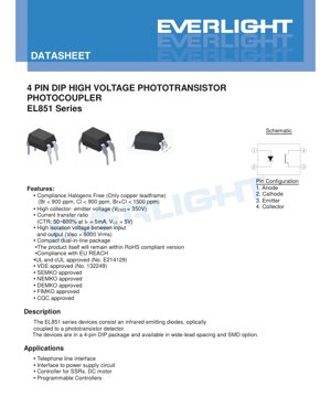
1. उत्पाद अवलोकन
EL851 श्रृंखला उच्च वोल्टेज फोटोट्रांजिस्टर ऑप्टोकपलर का एक वर्ग है जो कठोर अनुप्रयोगों में मजबूत विद्युत इन्सुलेशन के लिए डिज़ाइन किया गया है। ये उपकरण एक अवरक्त उत्सर्जक डायोड को एकीकृत करते हैं, जो एक सिलिकॉन फोटोट्रांजिस्टर डिटेक्टर के साथ ऑप्टिकली युग्मित है और एक कॉम्पैक्ट 4-पिन ड्यूल इन-लाइन पैकेज (DIP) में संलग्न है। इनका प्राथमिक कार्य प्रकाश का उपयोग करके दो पृथक सर्किट के बीच विद्युत संकेतों का संचार करना है, जिससे उच्च वोल्टेज या शोर आउटपुट साइड से इनपुट साइड या इसके विपरीत प्रसारित होने से रोका जा सके। यह श्रृंखला अपने उच्च कलेक्टर-एमिटर वोल्टेज रेटिंग की विशेषता से प्रतिष्ठित है, जो इसे पावर सप्लाई सर्किट और अन्य उच्च वोल्टेज प्रणालियों के साथ इंटरफेस के लिए उपयुक्त बनाती है।
1.1 मुख्य लाभ एवं लक्षित बाजार
EL851 श्रृंखला कई महत्वपूर्ण लाभ प्रदान करती है, जो बाजार में इसकी स्थिति को स्थापित करते हैं। इसकी सबसे उल्लेखनीय विशेषताVCEO350V की रेटिंग है, जो इसे इनपुट और आउटपुट पक्षों के बीच महत्वपूर्ण वोल्टेज अंतर को सहन करने में सक्षम बनाती है। यहVISO5000 Vrmsउच्च विद्युत पृथक्करण वोल्टेज (Vrms), जो औद्योगिक और दूरसंचार उपकरणों में एक विश्वसनीय सुरक्षा अवरोध प्रदान करने की गारंटी देता है। ये उपकरण UL, cUL, VDE सहित प्रमुख अंतरराष्ट्रीय सुरक्षा मानकों और विभिन्न अन्य क्षेत्रीय प्रमाणनों (SEMKO, NEMKO, DEMKO, FIMKO, CQC) का अनुपालन करते हैं, जिससे वैश्विक बाजार में उनकी पहुंच सुगम होती है। इसके अतिरिक्त, यह श्रृंखला हलोजन-मुक्त (कॉपर लीड फ्रेम संस्करण के लिए) के रूप में डिज़ाइन की गई है और RoHS तथा यूरोपीय संघ के REACH विनियमों का अनुपालन करती है, जो आधुनिक पर्यावरणीय और नियामक आवश्यकताओं को पूरा करती है। लक्षित अनुप्रयोगों में टेलीफोन लाइन इंटरफेस, बिजली आपूर्ति सर्किट इंटरफेस, सॉलिड-स्टेट रिले (SSR) और डीसी मोटर नियंत्रक, साथ ही प्रोग्रामेबल कंट्रोलर शामिल हैं जहां सिग्नल पृथक्करण और शोर प्रतिरोध क्षमता महत्वपूर्ण है।
2. गहन तकनीकी मापदंड विश्लेषण
सही सर्किट डिजाइन और विश्वसनीय संचालन के लिए उपकरण की विद्युत और प्रकाशीय विशेषताओं की गहन समझ महत्वपूर्ण है।
2.1 पूर्ण अधिकतम रेटिंग
पूर्ण अधिकतम रेटिंग उन तनाव सीमाओं को परिभाषित करती है जो उपकरण की स्थायी क्षति का कारण बन सकती हैं। ये मान सामान्य संचालन स्थितियों के लिए नहीं हैं। EL851 की प्रमुख रेटिंग में शामिल हैं:
- इनपुट फॉरवर्ड करंट (IF)): 60 mA (निरंतर)।
- पीक फॉरवर्ड करंट (IFM)): 1 A (1µs पल्स अवधि), अल्पकालिक सर्ज स्थितियों के लिए उपयुक्त।
- कलेक्टर-एमिटर वोल्टेज (VCEO)): 350 V, यह बेस ओपन सर्किट पर आउटपुट ट्रांजिस्टर के पार लगाया जा सकने वाला अधिकतम वोल्टेज है।
- कलेक्टर करंट (IC)): 50 mA।
- कुल पावर डिसिपेशन (PTOT)): 200 mW, इनपुट और आउटपुट पावर सीमाओं का संयोजन।
- आइसोलेशन वोल्टेज (VISO)): 5000 Vrms(40-60% सापेक्ष आर्द्रता पर 1 मिनट के लिए)। यह परीक्षण पिन 1 और 2 शॉर्टेड, पिन 3 और 4 शॉर्टेड की स्थिति में किया गया।
- ऑपरेटिंग तापमान (TOPR)): -55°C से +100°C।
- सोल्डरिंग तापमान (TSOL)): 260°C पर 10 सेकंड के लिए, वेव सोल्डरिंग या रीफ्लो सोल्डरिंग प्रक्रियाओं के लिए उपयुक्त।
2.2 ऑप्टोइलेक्ट्रॉनिक विशेषताएँ
ये पैरामीटर आमतौर पर 25°C पर निर्दिष्ट किए जाते हैं और डिवाइस के सामान्य संचालन स्थितियों में प्रदर्शन का वर्णन करते हैं।
2.2.1 इनपुट विशेषताएँ (LED पक्ष)
- फॉरवर्ड वोल्टेज (VF)): टाइपिकल 1.2V, IF= 10 mA पर अधिकतम 1.4V। इसका उपयोग इनपुट पक्ष पर आवश्यक करंट-लिमिटिंग रेसिस्टर की गणना के लिए किया जाता है।
- रिवर्स करंट (IR)): VR=5V पर अधिकतम 10 µA, यह दर्शाता है कि LED रिवर्स बायस्ड होने पर लीकेज करंट बहुत कम है।
- इनपुट कैपेसिटेंस (Cin)): टाइपिकल 30 pF, अधिकतम 250 pF। यह इनपुट साइड के हाई-फ़्रीक्वेंसी स्विचिंग परफॉर्मेंस को प्रभावित कर सकता है।
2.2.2 आउटपुट विशेषताएँ (फोटोट्रांजिस्टर पक्ष)
- कलेक्टर-एमिटर डार्क करंट (ICEO)): VCE=200V पर अधिकतम 100 nA। यह LED बंद (बिना प्रकाश) होने पर का लीकेज करंट है, जो "ऑफ स्टेट" सिग्नल इंटीग्रिटी निर्धारित करने के लिए महत्वपूर्ण है।
- कलेक्टर-एमिटर ब्रेकडाउन वोल्टेज (BVCEO)): I मेंC= 0.1mA पर न्यूनतम 350V, इसकी उच्च वोल्टेज क्षमता की पुष्टि करता है।
- कलेक्टर-एमिटर कैपेसिटेंस (CCE)): VCE= 0V पर विशिष्ट रूप से 10 pF है।
2.2.3 ट्रांसमिशन विशेषताएँ
- करंट ट्रांसफर रेशियो (CTR)): I मेंF= 5mA और VCE= 5V पर, 50% से 600% तक की सीमा में। CTR को (IC/ I के रूप में परिभाषित किया गया है।F)* 100%. उच्च CTR किसी दिए गए आउटपुट करंट को चलाने के लिए कम इनपुट करंट का उपयोग करने की अनुमति देता है, जिससे दक्षता बढ़ जाती है। व्यापक रेंज इंगित करती है कि एक बिनिंग प्रणाली मौजूद है; डिजाइनरों को सुनिश्चित करने के लिए सर्किट में न्यूनतम CTR पर विचार करना चाहिए कि यह ठीक से काम करे।
- कलेक्टर-एमिटर संतृप्ति वोल्टेज (VCE(sat))): I मेंF= 20mA और IC= 1mA पर अधिकतम 0.4V। जब फोटोट्रांजिस्टर को "ऑन" अवस्था में एक स्विच के रूप में उपयोग किया जाता है, तो यह कम संतृप्ति वोल्टेज बहुत महत्वपूर्ण होता है, क्योंकि यह वोल्टेज ड्रॉप और पावर लॉस को कम करता है।
- इंसुलेशन प्रतिरोध (RIO)): V11= 500V DC पर न्यूनतम 10IOΩ, जो इनपुट और आउटपुट के बीच उत्कृष्ट डीसी अलगाव को दर्शाता है।
- इनपुट-आउटपुट कैपेसिटेंस (CIO)): टाइपिकल 0.6 pF, बहुत कम, जो हाई-फ़्रीक्वेंसी शोर के आइसोलेशन बैरियर के माध्यम से कैपेसिटिव कपलिंग को न्यूनतम करने में सहायता करता है।
- राइज़ टाइम (tr) और फ़ॉल टाइम (tf)): टाइपिकल क्रमशः 4 µs और 5 µs, टेस्ट कंडीशन (VCE=2V, IC=2mA, RL=100Ω) के तहत अधिकतम प्रत्येक 18 µs। ये पैरामीटर ऑप्टोकपलर की स्विचिंग गति को परिभाषित करते हैं, जो डिजिटल सिग्नल ट्रांसमिशन या PWM एप्लिकेशन के लिए महत्वपूर्ण हैं।
3. प्रदर्शन वक्र विश्लेषण
हालांकि विशिष्ट ग्राफिकल डेटा PDF में संदर्भित है (विशिष्ट ऑप्टोइलेक्ट्रॉनिक विशेषता वक्र, चित्र 9), लेकिन महत्वपूर्ण व्याख्या प्रदान की गई तालिका डेटा और परीक्षण सर्किट पर आधारित है।
स्विचिंग समय परीक्षण सर्किट एक मानक विन्यास दिखाता है, जहां पल्स करंट इनपुट LED को चलाता है, और लोड रेसिस्टर (RL) पर आउटपुट फोटोट्रांजिस्टर की प्रतिक्रिया मापी जाती है। राइज टाइम (tr) वह समय है जब LED चालू होने पर आउटपुट करंट अपने अंतिम मान के 10% से 90% तक बढ़ने में लेता है। फॉल टाइम (tf) वह समय है जब LED बंद होने पर 90% से 10% तक गिरने में लेता है। 4-5 µs सीमा में विशिष्ट मान बताते हैं कि यह डिवाइस मध्यम गति स्विचिंग अनुप्रयोगों के लिए उपयुक्त है, जैसे रिले ड्राइव या कम आवृत्ति डेटा लाइन अलगाव, लेकिन बहुत उच्च गति डिजिटल संचार के लिए उपयुक्त नहीं हो सकता है।
4. यांत्रिक एवं पैकेजिंग जानकारी
4.1 पैकेज आयाम एवं विकल्प
EL851 तीन मुख्य पिन फॉर्म विकल्प प्रदान करता है, प्रत्येक की विशिष्ट आयाम और अनुप्रयोग हैं।
- Standard DIP Type: Default through-hole package.
- M Type Option: Features wide pin bends with a pin pitch of 0.4 inches (approximately 10.16mm), suitable for circuit boards requiring wider pin spacing.
- S1 Type Option: A low-profile surface-mount (SMD) pin form. This is the SMD variant of the device.
Although the PDF drawing provides precise numerical dimensions, the overall package size of the standard DIP type is approximately 6.35mm in length, 4.57mm in width, and 3.3mm in height, making it a compact component.
4.2 ध्रुवीयता पहचान एवं अंकन
पिन विन्यास मानकीकृत है:
- एनोड (इनपुट LED का धनात्मक टर्मिनल)
- कैथोड (इनपुट LED का ऋणात्मक टर्मिनल)
- एमिटर (फोटोट्रांजिस्टर एमिटर, आमतौर पर आउटपुट साइड के ग्राउंड/कॉमन से जुड़ा)
- कलेक्टर (फोटोट्रांजिस्टर कलेक्टर, आउटपुट टर्मिनल)
डिवाइस के शीर्ष पर "EL" (निर्माता को दर्शाता है), "851" (डिवाइस संख्या), उसके बाद एक अंक का वर्ष कोड (Y), दो अंकों का सप्ताह कोड (WW), और वैकल्पिक रूप से VDE प्रमाणित संस्करण को दर्शाने के लिए "V" अंकित होता है। पिन 1 की सही पहचान (आमतौर पर पैकेज पर एक बिंदु, खांचे या बेवल किनारे द्वारा इंगित) असेंबली के दौरान सही अभिविन्यास के लिए महत्वपूर्ण है।
4.3 अनुशंसित पैड लेआउट
S1 (सरफेस माउंट) विकल्प के लिए, एक अनुशंसित पैड लेआउट प्रदान किया गया है। सुझाए गए आयाम केवल संदर्भ के लिए हैं; विश्वसनीय सोल्डर जोड़ सुनिश्चित करने के लिए, डिजाइनरों को अपनी विशिष्ट PCB निर्माण प्रक्रिया, सोल्डर पेस्ट एप्लिकेशन और थर्मल प्रबंधन आवश्यकताओं के आधार पर इन्हें संशोधित करने की सलाह दी जाती है।
5. सोल्डरिंग और असेंबली गाइड
यह डिवाइस अधिकतम 260°C तक, 10 सेकंड तक की सोल्डरिंग तापमान का सामना कर सकता है। यह थ्रू-होल पैकेज के लिए मानक वेव सोल्डरिंग और SMD विकल्प के लिए लीड-फ्री रीफ्लो प्रोफाइल के साथ संगत है। आंतरिक डाई, बॉन्डिंग वायर या प्लास्टिक पैकेज सामग्री को नुकसान से बचाने के लिए इस समय-तापमान सीमा का सख्ती से पालन करना महत्वपूर्ण है। हैंडलिंग और असेंबली के दौरान मानक ESD (इलेक्ट्रोस्टैटिक डिस्चार्ज) सावधानियों का पालन किया जाना चाहिए। भंडारण तापमान सीमा -55°C से +125°C है।
6. पैकेजिंग और ऑर्डर जानकारी
6.1 मॉडल नंबरिंग नियम
पुर्जा संख्या निम्नलिखित प्रारूप का पालन करती है:EL851X(Z)-V.
- X: पिन कॉन्फ़िगरेशन विकल्प।
- कोई नहीं: मानक DIP-4 (100/ट्यूब)।
- M: चौड़ी पिन बेंड, 0.4" पिच (100/ट्यूब)।
- S1: सतह माउंट पिन कॉन्फ़िगरेशन (लो प्रोफाइल)।
- Z: रील पैकेजिंग विकल्प (केवल S1 के लिए)।
- TA, TB, TU, TD: विभिन्न रील फॉर्मेट, जो पैकेजिंग मात्रा (1000 या 1500 टुकड़े/रील) को प्रभावित करते हैं।
- V: वैकल्पिक प्रत्यय, VDE सुरक्षा प्रमाणन को दर्शाता है।
6.2 रील टेप विनिर्देश
S1 विकल्प के लिए विस्तृत रील आयाम (A, B, D0, D1, E, F, P0, P1, P2, t, W, K) प्रदान करता है। ये आयाम PCB असेंबली मशीन द्वारा रील से घटकों को सही ढंग से उठाने और रखने के लिए महत्वपूर्ण हैं। रील की चौड़ाई (W) 16.0mm ±0.3mm है, और पॉकेट पिच (P0) 4.0mm ±0.1mm है।
7. अनुप्रयोग नोट एवं डिज़ाइन विचार
7.1 विशिष्ट अनुप्रयोग सर्किट
EL851 निम्नलिखित प्रमुख अनुप्रयोगों के लिए आदर्श रूप से अनुकूल है:
- टेलीफोन लाइन इंटरफेस: मॉडेम या टेलीफोन सिस्टम के संवेदनशील लॉजिक सर्किट को टेलीफोन लाइन पर उच्च वोल्टेज रिंगिंग सिग्नल और संभावित सर्ज से अलग करना।
- पावर सप्लाई फीडबैक लूप: स्विच्ड-मोड पावर सप्लाई (SMPS) में आउटपुट वोल्टेज का आइसोलेटेड फीडबैक प्रदान करना, प्राइमरी (उच्च वोल्टेज) साइड और सेकेंडरी (निम्न वोल्टेज) साइड के बीच सुरक्षित अलगाव बनाए रखते हुए वोल्टेज रेगुलेशन हासिल करना।
- SSR और DC मोटर नियंत्रण: सॉलिड-स्टेट रिले के गेट या इनपुट को ड्राइव करना, या माइक्रोकंट्रोलर और मोटर ड्राइव एच-ब्रिज के बीच एक आइसोलेशन इंटरफेस के रूप में कार्य करना, ताकि लॉजिक कंट्रोलर को मोटर के कारण होने वाले शोर और वोल्टेज स्पाइक्स से बचाया जा सके।
- प्रोग्रामेबल कंट्रोलर (PLC) I/O मॉड्यूलडिजिटल इनपुट/आउटपुट चैनलों को अलग करें, ताकि केंद्रीय प्रसंस्करण इकाई को फील्ड वायरिंग दोषों, शोर और विभिन्न ग्राउंड पोटेंशियल से बचाया जा सके।
7.2 प्रमुख डिज़ाइन कारक
- CTR क्षयऑप्टोकपलर का CTR समय के साथ क्षीण हो जाता है, विशेष रूप से उच्च तापमान और उच्च LED धारा पर संचालित होने पर। दीर्घकालिक विश्वसनीयता के लिए, सर्किट को उचित क्षय मार्जिन (आमतौर पर उत्पाद जीवनकाल में 50%) को ध्यान में रखने के बाद भी कार्य करने के लिए डिज़ाइन किया जाना चाहिए।न्यूनतमनिर्दिष्ट CTR सामान्य संचालन।
- इनपुट धारा सीमाफॉरवर्ड करंट (I) को सीमित करने के लिए इनपुट LED के साथ श्रृंखला में एक बाहरी प्रतिरोधक का उपयोग हमेशा किया जाना चाहिए।F) को सुरक्षित मूल्य तक सीमित करें, जो आमतौर पर 60mA के पूर्ण अधिकतम मूल्य से काफी कम होता है। प्रतिरोध मान की गणना R के रूप में की जाती है।सीमा= (Vआपूर्ति- वीF) / मैंF.
- आउटपुट लोड प्रतिरोधफोटोट्रांजिस्टर के कलेक्टर से जुड़े लोड रेसिस्टर (RLका मान आउटपुट वोल्टेज स्विंग और स्विचिंग स्पीड को प्रभावित करता है। छोटा RLउच्च गति की अनुमति देता है, लेकिन आउटपुट वोल्टेज लाभ कम कर देता है। RL=100Ω का परीक्षण शर्त निर्दिष्ट स्विचिंग समय के लिए एक संदर्भ प्रदान करती है।
- शोर प्रतिरोध क्षमता: हालांकि यह डिवाइस उत्कृष्ट विद्युत इन्सुलेशन प्रदान करता है, लेकिन अत्यंत कम इनपुट-आउटपुट कैपेसिटेंस (0.6 pF) उच्च आवृत्ति शोर युग्मन को न्यूनतम करने में मदद करता है। अत्यधिक शोर वाले वातावरण के लिए, इनपुट और आउटपुट सिग्नल पर अतिरिक्त फ़िल्टरिंग जोड़ने की आवश्यकता हो सकती है।
- ताप अपव्यय: कुल बिजली अपव्यय (PTOT= VF*IF+ VCE*IC) 200 mW से अधिक नहीं, साथ ही अधिकतम कार्य परिवेश तापमान पर विचार करें। 25°C से अधिक तापमान पर डीरेटिंग की आवश्यकता हो सकती है।
8. तकनीकी तुलना एवं विभेदीकरण
मानक निम्न-वोल्टेज ऑप्टोकपलर (आमतौर पर VCEOरेटिंग 30-70V) की तुलना में, EL851 की 350V रेटिंग इसकी प्रमुख विभेदक विशेषता है। यह इसे सीधे ऑफलाइन पावर सप्लाई फीडबैक सर्किट (जहां रेक्टिफाइड मेन्स वोल्टेज लगभग 300V+ हो सकता है) या औद्योगिक नियंत्रण इंटरफेस में उपयोग करने की अनुमति देता है, बिना आउटपुट साइड पर अतिरिक्त वोल्टेज क्लैम्प या स्टेप-डाउन सर्किट जोड़े। इसकी विस्तृत CTR रेंज संवेदनशील और मानक ड्राइव आवश्यकताओं के लिए विकल्प प्रदान करती है। थ्रू-होल (DIP, वाइड बेंड) और सरफेस माउंट (S1) रील पैकेजिंग दोनों उपलब्ध होने के कारण, यह प्रोटोटाइपिंग और बड़े पैमाने पर स्वचालित असेंबली दोनों के लिए उपयुक्त है, जिससे इसकी उपयोगिता बहुमुखी है।
9. सामान्य प्रश्नोत्तर (तकनीकी मापदंडों पर आधारित)
- प्रश्न: मुझे डिजाइन के लिए न्यूनतम CTR का कितना मान लेना चाहिए?
- उत्तर: हमेशा अपनी अपेक्षित कार्य IFऔर VCEअपने सर्किट को न्यूनतम CTR 50% के तहत डिज़ाइन करें। और उत्पाद के जीवनकाल में संभावित क्षीणता पर विचार करें।
- प्रश्न: क्या मैं इस ऑप्टोकपलर से सीधे 120VAC लोड स्विच कर सकता हूँ?
- उत्तर: नहीं। VCEOरेटिंग 350V DC है। 120VAC का पीक वोल्टेज लगभग 170V है, जो रेटिंग के भीतर है, लेकिन ऑप्टोकपलर का फोटोट्रांजिस्टर सीधे AC लोड की बड़ी धाराओं को संभालने के लिए डिज़ाइन नहीं किया गया है। इसका उपयोग स्वतंत्र उच्च-शक्ति स्विच (जैसे ट्रायक, MOSFET या SSR) के नियंत्रण इनपुट को चलाने के लिए किया जाना चाहिए।
- प्रश्न: VCEOऔर VISO?
- में क्या अंतर है?CEOउत्तर: VISO(350V) आउटपुट ट्रांजिस्टर के कलेक्टर और एमिटर पिन के बीच लगाया जा सकने वाला अधिकतम डीसी वोल्टेज है। V(5000 Vrms
- ) शॉर्टेड इनपुट पिन (1,2) और शॉर्टेड आउटपुट पिन (3,4) के बीच परीक्षण किया गया एसी विद्युतरोधन वोल्टेज है, जो आंतरिक प्लास्टिक बैरियर की अलगाव शक्ति का प्रतिनिधित्व करता है।
- प्रश्न: DIP और SMD पैकेजिंग के बीच कैसे चयन करें?
उत्तर: प्रोटोटाइप निर्माण, मैन्युअल असेंबली, या ऐसे अनुप्रयोगों के लिए जहां सर्किट बोर्ड स्थान की अधिक आवश्यकता नहीं है और पिन थ्रू-होल सोल्डरिंग की यांत्रिक शक्ति चाहिए, थ्रू-होल DIP पैकेज का उपयोग करें। स्वचालित असेंबली, उच्च घनत्व PCB डिजाइन और बोर्ड मोटाई कम करने की आवश्यकताओं के लिए, SMD (S1) पैकेज चुनें।
10. व्यावहारिक डिज़ाइन उदाहरण
परिदृश्य: 24V औद्योगिक सेंसर के लिए पृथक डिजिटल इनपुट।लक्ष्य:
24V प्रॉक्सिमिटी सेंसर को 3.3V माइक्रोकंट्रोलर से जोड़ना, 24V लाइन पर वोल्टेज ट्रांजिएंट से MCU की सुरक्षा के लिए पृथक्करण प्रदान करना।
- सर्किट डिज़ाइन:इनपुट साइड:सेंसर आउटपुट (सिंक करंट प्रकार) +24V और EL851 के एनोड (पिन 1) के बीच जुड़ा हुआ है। एक करंट-लिमिटिंग रेसिस्टर (Rin) कैथोड (पिन 2) और ग्राउंड के बीच रखा जाता है। जब सेंसर सक्रिय होता है, तो RinFका चयन IFको नाममात्र 5-10 mA पर सेट करने के लिए किया जाता है। उदाहरण के लिए, यदि V~1.2V है, तो Rin
- = (24V - 1.2V) / 0.005A ≈ 4.56kΩ (4.7kΩ मानक मान का उपयोग करें)।आउटपुट साइड:फोटोट्रांजिस्टर कलेक्टर (पिन 4) एक पुल-अप रोकनेवाला (Rpullup) के माध्यम से 3.3V MCU पावर से जुड़ा है। एमिटर (पिन 3) MCU ग्राउंड से जुड़ा है। जब सेंसर सक्रिय होता है, तो LED जलती है, फोटोट्रांजिस्टर संतृप्त हो जाता है, और कलेक्टर (आउटपुट सिग्नल) को निम्न (लगभग 0.4V) खींचता है। जब सेंसर बंद होता है, तो फोटोट्रांजिस्टर बंद हो जाता है, Rpullupआउटपुट को 3.3V तक उच्च खींचता है। आवश्यक गति और बिजली खपत के आधार पर Rpullup
- का चयन करें; 1kΩ से 10kΩ सामान्य मान हैं।इन्सुलेशन:24V सेंसर ग्राउंड और 3.3V MCU ग्राउंड पूरी तरह से अलग हैं। EL851 का 5000Vrms
यह सरल सर्किट मजबूत पृथक डिजिटल सिग्नल ट्रांसमिशन प्रदान करता है।
11. कार्य सिद्धांतFEEL851 फोटोइलेक्ट्रिक रूपांतरण और अलगाव के सिद्धांत पर काम करता है। इनपुट साइड पर लगाया गया करंट इन्फ्रारेड लाइट एमिटिंग डायोड (LED) से होकर बहता है, जिससे वह प्रकाशित होता है। यह प्रकाश प्लास्टिक एनकैप्सुलेशन के भीतर एक पारदर्शी अलगाव अंतराल को पार करता है और आउटपुट साइड पर सिलिकॉन फोटोट्रांजिस्टर के बेस क्षेत्र पर पड़ता है। आपतित प्रकाश बेस क्षेत्र में इलेक्ट्रॉन-होल युग्म उत्पन्न करता है, जो प्रभावी रूप से बेस करंट का कार्य करता है। इस फोटोजेनरेटेड बेस करंट को ट्रांजिस्टर के करंट गेन (hC) द्वारा प्रवर्धित किया जाता है, जिससे एक बड़ा कलेक्टर करंट (I
). इस आउटपुट कलेक्टर करंट और इनपुट LED करंट के अनुपात को करंट ट्रांसफर रेशियो (CTR) कहा जाता है। इनपुट और आउटपुट सर्किट के बीच कोई विद्युत कनेक्शन नहीं है; केवल प्रकाश उन्हें युग्मित करता है, जिससे विद्युत पृथक्करण प्रदान होता है।
12. तकनीकी रुझान
LED विनिर्देशन शब्दावली का विस्तृत विवरण
एलईडी तकनीकी शब्दावली की पूर्ण व्याख्या
एक, प्रकाशविद्युत प्रदर्शन के मुख्य मापदंड
| शब्दावली | इकाई/प्रतिनिधित्व | सामान्य व्याख्या | यह महत्वपूर्ण क्यों है |
|---|---|---|---|
| दीप्त प्रभावकारिता (Luminous Efficacy) | lm/W (लुमेन प्रति वाट) | प्रति वाट विद्युत ऊर्जा से उत्सर्जित दीप्त प्रवाह, जितना अधिक होगा उतनी ही अधिक ऊर्जा बचत होगी। | यह सीधे तौर पर प्रकाश उपकरण की ऊर्जा दक्षता श्रेणी और बिजली लागत निर्धारित करता है। |
| दीप्त प्रवाह (Luminous Flux) | lm (लुमेन) | प्रकाश स्रोत द्वारा उत्सर्जित कुल प्रकाश मात्रा, जिसे आम बोलचाल में "चमक" कहा जाता है। | यह निर्धारित करता है कि लैंप पर्याप्त रूप से चमकीला है या नहीं। |
| प्रकाश उत्सर्जन कोण (Viewing Angle) | ° (डिग्री), जैसे 120° | वह कोण जिस पर प्रकाश तीव्रता आधी रह जाती है, यह प्रकाश पुंज की चौड़ाई निर्धारित करता है। | यह प्रकाश के प्रसार क्षेत्र और एकरूपता को प्रभावित करता है। |
| रंग तापमान (CCT) | K (केल्विन), जैसे 2700K/6500K | प्रकाश के रंग की गर्माहट या ठंडक, कम मान पीला/गर्म, उच्च मान सफेद/ठंडा। | प्रकाश व्यवस्था का माहौल और उपयुक्त परिदृश्य तय करता है। |
| रंग प्रतिपादन सूचकांक (CRI / Ra) | कोई इकाई नहीं, 0–100 | वस्तु के वास्तविक रंग को पुनः प्रस्तुत करने की प्रकाश स्रोत की क्षमता, Ra≥80 उत्तम है। | रंग सत्यता को प्रभावित करता है, शॉपिंग मॉल, आर्ट गैलरी आदि उच्च आवश्यकता वाले स्थानों के लिए उपयोग किया जाता है। |
| क्रोमैटिसिटी टॉलरेंस (SDCM) | मैकएडम एलिप्स स्टेप्स, जैसे "5-step" | रंग एकरूपता का मात्रात्मक सूचक, स्टेप्स जितने कम होंगे, रंग उतने ही अधिक एकसमान होंगे। | यह सुनिश्चित करता है कि एक ही बैच के लैंपों के रंग में कोई अंतर न हो। |
| प्रमुख तरंगदैर्ध्य (Dominant Wavelength) | nm (नैनोमीटर), उदाहरण के लिए 620nm (लाल) | रंगीन LED रंग के अनुरूप तरंगदैर्ध्य मान। | लाल, पीले, हरे आदि मोनोक्रोमैटिक LED के रंगत (ह्यू) को निर्धारित करता है। |
| स्पेक्ट्रम वितरण (Spectral Distribution) | तरंगदैर्ध्य बनाम तीव्रता वक्र | LED द्वारा उत्सर्जित प्रकाश की विभिन्न तरंगदैर्ध्य पर तीव्रता वितरण प्रदर्शित करता है। | रंग प्रतिपादन और रंग गुणवत्ता को प्रभावित करता है। |
दो, विद्युत मापदंड
| शब्दावली | प्रतीक | सामान्य व्याख्या | डिज़ाइन विचार |
|---|---|---|---|
| फॉरवर्ड वोल्टेज (Forward Voltage) | Vf | LED को चालू करने के लिए आवश्यक न्यूनतम वोल्टेज, एक "स्टार्ट-अप थ्रेशोल्ड" के समान। | ड्राइव पावर सप्लाई वोल्टेज ≥ Vf होना चाहिए, कई LEDs को श्रृंखला में जोड़ने पर वोल्टेज जुड़ जाता है। |
| फॉरवर्ड करंट (Forward Current) | If | वह करंट मान जो LED को सामान्य रूप से चमकने के लिए आवश्यक है। | स्थिर धारा ड्राइव का उपयोग आम है, धारा चमक और आयु निर्धारित करती है। |
| अधिकतम स्पंद धारा (Pulse Current) | Ifp | अल्प अवधि में सहन करने योग्य शिखर धारा, डिमिंग या फ्लैश के लिए उपयोग की जाती है। | स्पंद चौड़ाई और ड्यूटी साइकल को सख्ती से नियंत्रित किया जाना चाहिए, अन्यथा अत्यधिक गर्मी से क्षति होगी। |
| रिवर्स वोल्टेज (Reverse Voltage) | Vr | LED द्वारा सहन की जा सकने वाली अधिकतम रिवर्स वोल्टेज, इससे अधिक होने पर ब्रेकडाउन हो सकता है। | सर्किट में रिवर्स कनेक्शन या वोल्टेज स्पाइक को रोकने की आवश्यकता है। |
| थर्मल रेजिस्टेंस (Thermal Resistance) | Rth (°C/W) | चिप से सोल्डर पॉइंट तक गर्मी के प्रवाह का प्रतिरोध, कम मान बेहतर हीट डिसिपेशन दर्शाता है। | उच्च तापीय प्रतिरोध के लिए मजबूत ऊष्मा अपव्यय डिज़ाइन आवश्यक है, अन्यथा जंक्शन तापमान बढ़ जाता है। |
| इलेक्ट्रोस्टैटिक डिस्चार्ज इम्यूनिटी (ESD Immunity) | V (HBM), जैसे 1000V | स्थैतिक बिजली के प्रति प्रतिरोधक क्षमता, उच्च मान का अर्थ है स्थैतिक क्षति से अधिक सुरक्षा। | उत्पादन में स्थैतिक बिजली सुरक्षा उपाय करने आवश्यक हैं, विशेष रूप से उच्च संवेदनशीलता वाले LED के लिए। |
तीन, ताप प्रबंधन और विश्वसनीयता
| शब्दावली | प्रमुख संकेतक | सामान्य व्याख्या | प्रभाव |
|---|---|---|---|
| जंक्शन तापमान (Junction Temperature) | Tj (°C) | एलईडी चिप के अंदर का वास्तविक कार्य तापमान। | प्रत्येक 10°C कमी से, जीवनकाल दोगुना हो सकता है; अत्यधिक तापमान से प्रकाश क्षय और रंग विस्थापन होता है। |
| ल्यूमेन डिप्रिसिएशन (Lumen Depreciation) | L70 / L80 (घंटे) | चमक प्रारंभिक मान के 70% या 80% तक गिरने में लगने वाला समय। | एलईडी के "उपयोगी जीवन" को सीधे परिभाषित करता है। |
| ल्यूमेन मेंटेनेंस (Lumen Maintenance) | % (जैसे 70%) | एक निश्चित अवधि के उपयोग के बाद शेष चमक का प्रतिशत। | दीर्घकालिक उपयोग के बाद चमक बनाए रखने की क्षमता को दर्शाता है। |
| Color Shift | Δu′v′ या MacAdam Ellipse | उपयोग के दौरान रंग में परिवर्तन की मात्रा। | प्रकाश व्यवस्था के दृश्य की रंग एकरूपता को प्रभावित करता है। |
| थर्मल एजिंग (Thermal Aging) | सामग्री प्रदर्शन में गिरावट | दीर्घकालिक उच्च तापमान के कारण एनकैप्सुलेशन सामग्री का क्षरण। | चमक में कमी, रंग परिवर्तन या ओपन-सर्किट विफलता का कारण बन सकता है। |
चार, पैकेजिंग और सामग्री
| शब्दावली | सामान्य प्रकार | सामान्य व्याख्या | विशेषताएं और अनुप्रयोग |
|---|---|---|---|
| एनकैप्सुलेशन प्रकार | EMC, PPA, सिरेमिक | चिप की सुरक्षा करने और प्रकाशिकी एवं ऊष्मीय इंटरफेस प्रदान करने वाली आवरण सामग्री। | EMC उच्च ताप सहनशील, कम लागत; सिरेमिक बेहतर ताप अपव्यय, लंबी आयु। |
| चिप संरचना | फॉरवर्ड माउंटेड, फ्लिप चिप (Flip Chip) | चिप इलेक्ट्रोड व्यवस्था विधि। | फ्लिप चिप में बेहतर हीट डिसिपेशन और उच्च प्रकाश दक्षता होती है, जो उच्च शक्ति के लिए उपयुक्त है। |
| फॉस्फर कोटिंग | YAG, सिलिकेट, नाइट्राइड | नीली रोशनी चिप पर लगाया जाता है, जो आंशिक रूप से पीली/लाल रोशनी में परिवर्तित होकर सफेद प्रकाश बनाता है। | विभिन्न फॉस्फोरस प्रकाश दक्षता, रंग तापमान और रंग प्रतिपादन को प्रभावित करते हैं। |
| लेंस/ऑप्टिकल डिज़ाइन | समतल, माइक्रोलेंस, पूर्ण आंतरिक परावर्तन | पैकेजिंग सतह की प्रकाशिक संरचना, जो प्रकाश वितरण को नियंत्रित करती है। | प्रकाश उत्सर्जन कोण और प्रकाश वितरण वक्र निर्धारित करता है। |
पाँच, गुणवत्ता नियंत्रण और ग्रेडिंग
| शब्दावली | ग्रेडिंग सामग्री | सामान्य व्याख्या | उद्देश्य |
|---|---|---|---|
| ल्यूमिनस फ्लक्स ग्रेडिंग | कोड जैसे 2G, 2H | चमक के स्तर के अनुसार समूहों में विभाजित, प्रत्येक समूह का न्यूनतम/अधिकतम लुमेन मान होता है। | यह सुनिश्चित करना कि एक ही बैच के उत्पादों की चमक एक समान हो। |
| वोल्टेज ग्रेडिंग | कोड जैसे 6W, 6X | फॉरवर्ड वोल्टेज रेंज के अनुसार समूहीकरण। | ड्राइव पावर मिलान की सुविधा, सिस्टम दक्षता में सुधार। |
| रंग ग्रेडिंग | 5-step MacAdam ellipse | रंग निर्देशांक के अनुसार समूहीकरण करें, यह सुनिश्चित करते हुए कि रंग अत्यंत सीमित सीमा के भीतर रहें। | रंग एकरूपता सुनिश्चित करें, एक ही प्रकाश स्रोत के भीतर रंग में असमानता से बचें। |
| Color temperature binning | 2700K, 3000K, आदि। | रंग तापमान के अनुसार समूहीकरण करें, प्रत्येक समूह की अपनी संबंधित निर्देशांक सीमा हो। | विभिन्न परिदृश्यों की रंग तापमान आवश्यकताओं को पूरा करना। |
छह, परीक्षण और प्रमाणन
| शब्दावली | मानक/परीक्षण | सामान्य व्याख्या | महत्व |
|---|---|---|---|
| LM-80 | लुमेन रखरखाव परीक्षण | निरंतर तापमान की स्थिति में लंबे समय तक जलाकर, चमक क्षय डेटा रिकॉर्ड करना। | एलईडी जीवनकाल का अनुमान लगाने के लिए (TM-21 के साथ संयुक्त)। |
| TM-21 | जीवनकाल प्रक्षेपण मानक | LM-80 डेटा के आधार पर वास्तविक उपयोग की स्थितियों में जीवनकाल का अनुमान लगाना। | वैज्ञानिक जीवनकाल पूर्वानुमान प्रदान करना। |
| IESNA मानक | Illuminating Engineering Society Standard | Optical, electrical, and thermal testing methods are covered. | Industry-recognized testing basis. |
| RoHS / REACH | Environmental Certification | Ensures the product does not contain harmful substances (such as lead, mercury). | अंतर्राष्ट्रीय बाजार में प्रवेश की पात्रता शर्तें। |
| ENERGY STAR / DLC | ऊर्जा दक्षता प्रमाणन | प्रकाश उत्पादों के लिए ऊर्जा दक्षता और प्रदर्शन प्रमाणन। | सामान्यतः सरकारी खरीद, सब्सिडी कार्यक्रमों में उपयोग किया जाता है, बाजार प्रतिस्पर्धा बढ़ाने के लिए। |