विषय-सूची
- 1. उत्पाद अवलोकन
- 2. तकनीकी विशिष्टताओं का गहन विश्लेषण
- 2.1 पूर्ण अधिकतम रेटिंग्स
- 2.2 विद्युत-प्रकाशीय विशेषताएँ
- 3. बिनिंग सिस्टम व्याख्या
- 4. Performance Curve Analysis
- 4.1 Radiant Intensity vs. Forward Current
- 4.2 फॉरवर्ड करंट बनाम फॉरवर्ड वोल्टेज
- 4.3 फॉरवर्ड करंट बनाम एम्बिएंट टेम्परेचर
- 4.4 स्पेक्ट्रल डिस्ट्रीब्यूशन
- 4.5 Relative Radiant Intensity vs. Angular Displacement
- 5. Mechanical and Package Information
- 6. Soldering and Assembly Guidelines
- 6.1 Storage and Moisture Sensitivity
- 6.2 रीफ्लो सोल्डरिंग
- 6.3 हाथ से सोल्डरिंग और पुनर्कार्य
- 6.4 सर्किट सुरक्षा
- 7. पैकेजिंग और ऑर्डर जानकारी
- 7.1 टेप और रील विनिर्देश
- 7.2 पैकिंग प्रक्रिया और लेबल
- 7.3 डिवाइस चयन गाइड
- 8. एप्लिकेशन डिज़ाइन सुझाव
- 8.1 विशिष्ट एप्लिकेशन सर्किट
- 8.2 ऑप्टिकल डिज़ाइन विचार
- 8.3 तापीय प्रबंधन
- 9. तकनीकी तुलना और विभेदन
- 10. अक्सर पूछे जाने वाले प्रश्न (तकनीकी मापदंडों के आधार पर)
- 10.1 रेडिएंट इंटेंसिटी (mW/sr) और रेडिएंट पावर (mW) में क्या अंतर है?
- 10.2 क्या मैं इस LED को 50mA पर लगातार चला सकता हूँ?
- 10.3 करंट-लिमिटिंग रेसिस्टर बिल्कुल आवश्यक क्यों है?
- 10.4 मैं "रैंक" (F, G, H, J) की व्याख्या कैसे करूं?
- 11. व्यावहारिक अनुप्रयोग उदाहरण
- 12. Operating Principle
- 13. Technology Trends
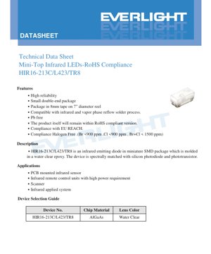
1. उत्पाद अवलोकन
The HIR16-213C/L423/TR8 एक उच्च विश्वसनीयता वाला, लघु सतह-माउंट डिवाइस (SMD) इन्फ्रारेड (IR) उत्सर्जक डायोड है। यह उन अनुप्रयोगों के लिए डिज़ाइन किया गया है जिन्हें आधुनिक स्वचालित असेंबली प्रक्रियाओं के साथ संगत एक कॉम्पैक्ट, कुशल इन्फ्रारेड स्रोत की आवश्यकता होती है। यह डिवाइस वाटर-क्लियर एपॉक्सी में ढाला गया है, जो एक मजबूत पैकेज प्रदान करता है और साथ ही इन्फ्रारेड प्रकाश के इष्टतम संचरण की अनुमति देता है।
मुख्य लाभ: The primary advantages of this component include its small double-ended package footprint, high reliability, and full compliance with environmental regulations such as RoHS, EU REACH, and halogen-free requirements (Br <900 ppm, Cl <900 ppm, Br+Cl < 1500 ppm). It is specifically spectrally matched with silicon photodiodes and phototransistors, making it ideal for sensing systems.
Target Market & Applications: यह आईआर एलईडी इलेक्ट्रॉनिक सिस्टम के डिजाइनरों और निर्माताओं को लक्षित करती है जिन्हें अवरक्त कार्यक्षमता की आवश्यकता है। मुख्य अनुप्रयोग क्षेत्रों में पीसीबी-माउंटेड अवरक्त सेंसर (निकटता या वस्तु पहचान के लिए), अवरक्त रिमोट कंट्रोल यूनिट (जहां उच्च विकिरण तीव्रता की आवश्यकता होती है), विभिन्न प्रकार के ऑप्टिकल स्कैनर और अन्य अवरक्त-आधारित प्रणालियाँ शामिल हैं।
2. तकनीकी विशिष्टताओं का गहन विश्लेषण
2.1 पूर्ण अधिकतम रेटिंग्स
ये रेटिंग्स उन सीमाओं को परिभाषित करती हैं जिनके बाहर डिवाइस को स्थायी क्षति हो सकती है। इन सीमाओं के बाहर संचालन की सलाह नहीं दी जाती है।
- Continuous Forward Current (IF): 50 mA. यह अधिकतम DC धारा है जो लगातार लगाई जा सकती है।
- Reverse Voltage (VR): 5 V. रिवर्स बायस में इस वोल्टेज से अधिक होने पर डायोड जंक्शन टूट सकता है।
- Operating & Storage Temperature (Topr, Tstg): -40°C से +100°C तक। यह व्यापक सीमा औद्योगिक और ऑटोमोटिव वातावरण के लिए उपयुक्तता सुनिश्चित करती है।
- Soldering Temperature (Tsol): 260°C for a maximum of 5 seconds, compatible with lead-free reflow profiles.
- Power Dissipation (Pc): 100 mW at or below 25°C ambient temperature. Derating is necessary at higher temperatures.
2.2 विद्युत-प्रकाशीय विशेषताएँ
These parameters are measured at a standard test condition of 25°C ambient temperature and a forward current of 20 mA, unless otherwise specified.
- Radiant Intensity (IE): Typical value is 1.50 mW/sr, with a minimum of 0.50 mW/sr. This measures the optical power emitted per unit solid angle.
- Peak Wavelength (λp): 850 nm (typical), ranging from 840 nm to 870 nm. This wavelength is near-optimal for silicon-based detectors.
- Spectral Bandwidth (Δλ): आमतौर पर 30 nm. यह अधिकतम तीव्रता के आधे पर स्पेक्ट्रल चौड़ाई को परिभाषित करता है।
- फॉरवर्ड वोल्टेज (VF): आमतौर पर 1.45V, IF=20mA पर अधिकतम 1.65V. 100mA (पल्स चौड़ाई ≤100μs, ड्यूटी ≤1%) की पल्स धारा पर, VF अधिकतम 2.00V तक बढ़ जाता है।
- रिवर्स करंट (IR): V पर अधिकतम 10 μAR=5V, जो अच्छी जंक्शन गुणवत्ता दर्शाता है।
- व्यू एंगल (2θ1/2): 145 डिग्री (सामान्य)। यह अत्यंत विस्तृत दृश्य कोण लेंस डिजाइन की विशेषता है, जो व्यापक उत्सर्जन प्रदान करता है।
3. बिनिंग सिस्टम व्याख्या
यह डिवाइस विभिन्न प्रदर्शन रैंकों में उपलब्ध है, मुख्य रूप से विकिरण तीव्रता के आधार पर। यह डिजाइनरों को उनकी विशिष्ट संवेदनशीलता या रेंज आवश्यकताओं के लिए उपयुक्त ग्रेड का चयन करने की अनुमति देता है।
- रैंक F: Radiant Intensity between 0.50 and 1.50 mW/sr at IF=20mA.
- Rank G: Radiant Intensity between 1.00 and 2.50 mW/sr.
- Rank H: 2.00 और 3.50 mW/sr के बीच विकिरण तीव्रता।
- Rank J: 3.00 और 4.50 mW/sr के बीच विकिरण तीव्रता।
मानक प्रस्ताव में फॉरवर्ड वोल्टेज या पीक वेवलेंथ के लिए कोई इंगित बिनिंग नहीं है, हालांकि इन मापदंडों के लिए निर्दिष्ट न्यूनतम/सामान्य/अधिकतम मान हैं।
4. Performance Curve Analysis
4.1 Radiant Intensity vs. Forward Current
प्रदत्त ग्राफ़ एक गैर-रैखिक संबंध दर्शाता है। रेडिएंट इंटेंसिटी फॉरवर्ड करंट के साथ बढ़ती है लेकिन थर्मल और दक्षता सीमाओं के कारण अंततः संतृप्त हो जाएगी। वांछित ऑप्टिकल आउटपुट प्राप्त करने के लिए आवश्यक ऑपरेटिंग करंट निर्धारित करने के लिए यह वक्र आवश्यक है।
4.2 फॉरवर्ड करंट बनाम फॉरवर्ड वोल्टेज
यह IV वक्र एक डायोड की मानक घातीय विशेषता प्रदर्शित करता है। 20mA पर 1.45V का विशिष्ट VF ड्राइविंग सर्किट डिज़ाइन (जैसे, श्रृंखला रोकनेवाला गणना) के लिए एक प्रमुख पैरामीटर है।
4.3 फॉरवर्ड करंट बनाम एम्बिएंट टेम्परेचर
डीरेटिंग वक्र दर्शाता है कि अधिकतम अनुमेय निरंतर फॉरवर्ड करंट परिवेश तापमान बढ़ने के साथ घटता है। दीर्घकालिक विश्वसनीयता सुनिश्चित करने के लिए यह महत्वपूर्ण है, विशेष रूप से उच्च-तापमान अनुप्रयोगों में। डिवाइस को पूरे तापमान सीमा में अपनी पूर्ण 50mA रेटिंग पर संचालित नहीं किया जा सकता है।
4.4 स्पेक्ट्रल डिस्ट्रीब्यूशन
स्पेक्ट्रल आउटपुट 850nm पर केंद्रित है जिसकी एक सामान्य बैंडविड्थ 30nm है। यह सामान्य सिलिकॉन फोटोडिटेक्टर्स के शिखर प्रतिसाद क्षेत्र से मेल खाता है, जिससे सिस्टम सिग्नल-टू-नॉइज़ अनुपात अधिकतम हो जाता है।
4.5 Relative Radiant Intensity vs. Angular Displacement
ध्रुवीय आरेख 145° के दृश्य कोण की पुष्टि करता है, जहाँ केंद्रीय अक्ष से ±72.5° पर तीव्रता अपने शिखर मान की आधी हो जाती है। उत्सर्जन प्रारूप लैम्बर्टियन के करीब प्रतीत होता है, जो व्यापक-क्षेत्र प्रकाशन के लिए उपयुक्त है।
5. Mechanical and Package Information
डिवाइस एक कॉम्पैक्ट "मिनी-टॉप" एसएमडी पैकेज का उपयोग करता है। डेटाशीट से प्रमुख आयामी नोट्स में शामिल हैं:
- सभी आयाम मिलीमीटर में हैं।
- अनिर्दिष्ट आयामों के लिए मानक सहनशीलता ±0.1mm है।
- पैकेज में सोल्डरिंग के दौरान यांत्रिक स्थिरता के लिए डबल-एंडेड डिज़ाइन है।
- वॉटर-क्लियर एपॉक्सी लेंस पैकेज बॉडी का अभिन्न अंग है।
ध्रुवीयता पहचान: कैथोड आमतौर पर पैकेज पर चिह्नित होता है, अक्सर एक हरे रंग के बिंदु, एक खांचे या एक छोटे लीड के साथ। सटीक चिह्नन योजना के लिए डेटाशीट आरेख से परामर्श करना चाहिए।
6. Soldering and Assembly Guidelines
6.1 Storage and Moisture Sensitivity
The device is moisture-sensitive (MSL). Precautions are critical:
- Do not open the moisture-proof bag until ready for use.
- खोलने से पहले भंडारण: ≤30°C / ≤90% RH। 1 वर्ष के भीतर उपयोग करें।
- खोलने के बाद भंडारण: ≤30°C / ≤60% RH। 168 घंटे (7 दिन) के भीतर उपयोग करें।
- यदि भंडारण समय सीमा से अधिक हो जाता है या नमी सोखने वाला पदार्थ नमी का संकेत देता है, तो रीफ्लो से पहले 60±5°C पर कम से कम 24 घंटे के लिए बेक करना आवश्यक है।
6.2 रीफ्लो सोल्डरिंग
यह घटक इन्फ्रारेड और वेपर फेज रीफ्लो प्रक्रियाओं के साथ संगत है।
- 260°C के शिखर वाला एक लीड-मुक्त तापमान प्रोफ़ाइल निर्दिष्ट है।
- रीफ्लो दो बार से अधिक नहीं किया जाना चाहिए।
- गर्म करने और ठंडा करने के दौरान पैकेज पर यांत्रिक तनाव से बचें।
- सोल्डरिंग के बाद पीसीबी को मोड़ें नहीं।
6.3 हाथ से सोल्डरिंग और पुनर्कार्य
यदि हाथ से सोल्डरिंग करना आवश्यक हो:
- Use a soldering iron with a tip temperature <350°C.
- प्रति टर्मिनल संपर्क समय ≤3 सेकंड तक सीमित करें।
- 25W से कम या बराबर पावर वाले सोल्डरिंग आयरन का उपयोग करें।
- Allow a cooling interval of >2 seconds between terminals.
- रीवर्क के लिए, दोनों टर्मिनलों को एक साथ गर्म करने और पैकेज को नुकसान से बचाने के लिए डुअल-हेड सोल्डरिंग आयरन की सिफारिश की जाती है। किसी भी रीवर्क के बाद डिवाइस की कार्यक्षमता हमेशा सत्यापित करें।
6.4 सर्किट सुरक्षा
महत्वपूर्ण: LED के साथ श्रृंखला में एक बाहरी करंट-सीमित रोकनेवाला का उपयोग अवश्य किया जाना चाहिए। फॉरवर्ड वोल्टेज का नकारात्मक तापमान गुणांक होता है, जिसका अर्थ है कि यदि उचित रूप से नियंत्रित नहीं किया गया तो करंट अनियंत्रित रूप से बढ़ सकता है। वोल्टेज में मामूली वृद्धि भी करंट में बड़ा परिवर्तन कर सकती है, जिससे तत्काल जलने का खतरा रहता है।
7. पैकेजिंग और ऑर्डर जानकारी
7.1 टेप और रील विनिर्देश
डिवाइस 7 इंच व्यास वाले रील पर 8mm कैरियर टेप में आपूर्ति की जाती है। प्रत्येक रील में 3000 टुकड़े होते हैं। कैरियर टेप के आयाम मानक SMD पिक-एंड-प्लेस उपकरणों के साथ संगतता सुनिश्चित करते हैं।
7.2 पैकिंग प्रक्रिया और लेबल
रील्स को डिसिकेंट के साथ एल्यूमीनियम नमी-रोधी बैग में पैक किया जाता है। बैग पर लेबल में ट्रेसबिलिटी और सही अनुप्रयोग के लिए महत्वपूर्ण जानकारी शामिल होती है:
- CPN (Customer's Part Number)
- P/N (Production Part Number: HIR16-213C/L423/TR8)
- QTY (Quantity)
- CAT (रैंक/बिन कोड, उदाहरणार्थ, F, G, H, J)
- HUE (पीक वेवलेंथ)
- LOT No. (मैन्युफैक्चरिंग लॉट नंबर)
- Production Origin
7.3 डिवाइस चयन गाइड
मॉडल नंबर HIR16-213C/L423/TR8 का डिकोडिंग इस प्रकार है: चिप सामग्री AlGaAs (एल्यूमीनियम गैलियम आर्सेनाइड) है, और लेंस का रंग वॉटर क्लियर है। "TR8" प्रत्यय 8mm टेप और रील पैकेजिंग को दर्शाता है।
8. एप्लिकेशन डिज़ाइन सुझाव
8.1 विशिष्ट एप्लिकेशन सर्किट
एक सामान्य ड्राइविंग सर्किट में, एलईडी को एक करंट-लिमिटिंग रेसिस्टर के साथ श्रृंखला में जोड़कर वोल्टेज सप्लाई (VCC) से कनेक्ट किया जाता है। रेसिस्टर का मान ओम के नियम का उपयोग करके गणना की जाती है: R = (VCC - VF) / IF. उदाहरण के लिए, VCC=5V, VF=1.45V, और IF=20mA, R = (5 - 1.45) / 0.02 = 177.5 Ω. एक मानक 180 Ω रेसिस्टर उपयुक्त होगा। उच्च धाराओं (जैसे, 100mA) पर स्पंदित संचालन के लिए, सुनिश्चित करें कि ड्राइवर (अक्सर एक ट्रांजिस्टर) शिखर धारा को संभाल सकता है और ड्यूटी साइकिल को अति निम्न (≤1%) रखा जाए ताकि अधिक गर्म होने से बचा जा सके।
8.2 ऑप्टिकल डिज़ाइन विचार
145° का विस्तृत दृश्य कोण इस LED को उन अनुप्रयोगों के लिए उत्कृष्ट बनाता है जिनमें व्यापक, विसरित प्रकाश व्यवस्था की आवश्यकता होती है, जैसे कि proximity sensors जिन्हें एक विस्तृत क्षेत्र को कवर करने की आवश्यकता होती है। लंबी दूरी या अधिक निर्देशित अनुप्रयोगों के लिए, किरण को समानांतर करने के लिए द्वितीयक प्रकाशिकी (लेंस) की आवश्यकता हो सकती है। water-clear लेंस न्यूनतम अवशोषण के साथ निकट-अवरक्त संचरण के लिए इष्टतम है।
8.3 तापीय प्रबंधन
हालांकि पैकेज छोटा है, लेकिन विशेष रूप से उच्च धाराओं या उच्च परिवेशी तापमान में शक्ति अपव्यय पर विचार किया जाना चाहिए। सुनिश्चित करें कि PCB पैड लेआउट पर्याप्त थर्मल रिलीफ प्रदान करता है और अधिकतम जंक्शन तापमान पार नहीं होता है। तापमान के विरुद्ध अग्र धारा के लिए डीरेटिंग वक्र प्राथमिक मार्गदर्शक है।
9. तकनीकी तुलना और विभेदन
मानक 5mm या 3mm थ्रू-होल IR LEDs की तुलना में, यह SMD डिवाइस महत्वपूर्ण लाभ प्रदान करता है:
- Size & Automation: लघु SMD पैकेज छोटे PCB डिज़ाइनों को सक्षम बनाता है और यह उच्च-गति स्वचालित पिक-एंड-प्लेस तथा रीफ्लो सोल्डरिंग के साथ पूरी तरह संगत है, जिससे असेंबली लागत कम होती है।
- देखने का कोण: एक SMD IR LED के लिए 145° का देखने का कोण असाधारण रूप से चौड़ा है, जो संकीर्ण बीम वाले कई प्रतिस्पर्धियों की तुलना में अधिक समान कवरेज प्रदान करता है।
- अनुपालन: RoHS, REACH और हैलोजन-मुक्त मानकों के साथ पूर्ण अनुपालन सख्त पर्यावरणीय नियमों वाले वैश्विक बाजारों के लिए उत्पादों के लिए एक प्रमुख अंतरकारक है।
- स्पेक्ट्रल मिलान: 850nm का शिखर जानबूझकर सिलिकॉन डिटेक्टरों से मेल खाता है, यह एक विशेषता है जो सभी सामान्य आईआर एलईडी में अनुकूलित नहीं हो सकती है।
10. अक्सर पूछे जाने वाले प्रश्न (तकनीकी मापदंडों के आधार पर)
10.1 रेडिएंट इंटेंसिटी (mW/sr) और रेडिएंट पावर (mW) में क्या अंतर है?
रेडिएंट इंटेंसिटी प्रति यूनिट सॉलिड एंगल (स्टेरेडियन) उत्सर्जित ऑप्टिकल पावर है। रेडिएंट पावर सभी दिशाओं में उत्सर्जित कुल ऑप्टिकल पावर है। ज्ञात इंटेंसिटी और व्यूइंग एंगल पैटर्न वाले LED के लिए, कुल पावर की गणना पूर्ण उत्सर्जन क्षेत्र पर इंटेंसिटी को इंटीग्रेट करके की जा सकती है। डेटाशीट इंटेंसिटी प्रदान करती है, जो किसी विशिष्ट दूरी और कोण पर डिटेक्टर पर इर्रडिएंस की गणना के लिए अधिक उपयोगी है।
10.2 क्या मैं इस LED को 50mA पर लगातार चला सकता हूँ?
आप इसे केवल 50mA DC पर चला सकते हैं यदि परिवेश का तापमान 25°C या उससे कम है और आपके पास पर्याप्त थर्मल मैनेजमेंट है। डिरेटिंग कर्व दर्शाता है कि अधिकतम अनुमत निरंतर करंट तापमान बढ़ने के साथ घटता है। पूर्ण तापमान रेंज में विश्वसनीय संचालन के लिए, कम करंट या पल्स्ड ऑपरेशन की सिफारिश की जाती है।
10.3 करंट-लिमिटिंग रेसिस्टर बिल्कुल आवश्यक क्यों है?
LED करंट-चालित उपकरण हैं, वोल्टेज-चालित नहीं। उनका V-I वक्र बहुत खड़ा होता है। फॉरवर्ड वोल्टेज में एक छोटी सी वृद्धि (तापमान या आपूर्ति भिन्नता के कारण) करंट में बहुत बड़ी, संभावित रूप से विनाशकारी वृद्धि का कारण बन सकती है। श्रृंखला रेसिस्टर नकारात्मक प्रतिक्रिया प्रदान करता है, जिससे ऑपरेटिंग पॉइंट स्थिर होता है।
10.4 मैं "रैंक" (F, G, H, J) की व्याख्या कैसे करूं?
रैंक रेडिएंट इंटेंसिटी के लिए एक बिनिंग कोड है। यह आपको अपने एप्लिकेशन के लिए गारंटीकृत न्यूनतम ऑप्टिकल आउटपुट वाला उपकरण चुनने की अनुमति देता है। उदाहरण के लिए, यदि आपके सेंसर को कम से कम 2.0 mW/sr की आवश्यकता है, तो आपको रैंक H या J निर्दिष्ट करनी चाहिए। कम रैंक (F या G) का उपयोग करने से ऐसा उपकरण मिल सकता है जो आपकी प्रणाली की संवेदनशीलता आवश्यकताओं को पूरा नहीं करता।
11. व्यावहारिक अनुप्रयोग उदाहरण
Design Case: Simple Proximity Sensor
Objective: संवेदक के 10 सेमी के भीतर कोई वस्तु आने पर पता लगाएं।
डिज़ाइन: HIR16-213C/L423/TR8 IR LED और एक मिलान करने वाला सिलिकॉन फोटोट्रांजिस्टर को PCB पर एक साथ, एक ही दिशा में रखें। LED को 20mA स्थिर धारा (गणना किए गए श्रृंखला प्रतिरोधक का उपयोग करके) से चलाएं। जब कोई वस्तु मौजूद नहीं होती है, तो IR प्रकाश दूर चला जाता है और फोटोट्रांजिस्टर को बहुत कम परावर्तित प्रकाश दिखाई देता है। जब कोई वस्तु संसूचन क्षेत्र में प्रवेश करती है, तो कुछ IR प्रकाश फोटोट्रांजिस्टर पर वापस परावर्तित होता है, जिससे इसका कलेक्टर धारा बढ़ जाती है। इस धारा परिवर्तन को एक तुलनित्र द्वारा प्रवर्धित और एक डिजिटल संकेत में परिवर्तित किया जा सकता है।
घटक चयन का तर्क: LED का 145° का विस्तृत दृश्य कोण एक व्यापक संसूचन क्षेत्र सुनिश्चित करता है। 850nm तरंगदैर्ध्य फोटोट्रांजिस्टर से अधिकतम प्रतिसाद क्षमता सुनिश्चित करती है। रैंक H या J LED का चयन उच्च विकिरण तीव्रता प्रदान करता है, जिससे परावर्तित प्रकाश की मात्रा बढ़ती है और संभावित रूप से संसूचन सीमा या विश्वसनीयता में वृद्धि होती है।
मुख्य गणनाएँ: ड्राइविंग रेसिस्टर मान (जैसा कि खंड 8.1 में गणना की गई है)। फोटोट्रांजिस्टर पर अपेक्षित सिग्नल स्तर वस्तु की परावर्तकता पर निर्भर करेगा और तुलनित्र (कम्पेरेटर) के थ्रेशोल्ड को सही ढंग से सेट करने के लिए इसे अनुभवजन्य रूप से अभिलक्षित (कैरेक्टराइज़) करने की आवश्यकता होगी।
12. Operating Principle
एक इन्फ्रारेड लाइट एमिटिंग डायोड (IR LED) एक अर्धचालक p-n जंक्शन डायोड है। जब एक फॉरवर्ड वोल्टेज लगाया जाता है, तो n-टाइप अर्धचालक से इलेक्ट्रॉन और p-टाइप अर्धचालक से होल जंक्शन के पार इंजेक्ट होते हैं। जब ये आवेश वाहक सक्रिय क्षेत्र (इस मामले में AlGaAs चिप) में पुनर्संयोजित होते हैं, तो ऊर्जा फोटॉन (प्रकाश) के रूप में मुक्त होती है। विशिष्ट सामग्री संरचना (AlGaAs) बैंडगैप ऊर्जा निर्धारित करती है, जो सीधे उत्सर्जित फोटॉन की तरंगदैर्ध्य को परिभाषित करती है—इस मामले में, लगभग 850 नैनोमीटर के निकट-इन्फ्रारेड स्पेक्ट्रम में। वाटर-क्लियर एपॉक्सी पैकेज चिप को एनकैप्सुलेट करता है, यांत्रिक सुरक्षा प्रदान करता है और उत्सर्जित प्रकाश के कोणीय वितरण को आकार देने के लिए प्राथमिक लेंस के रूप में कार्य करता है।
13. Technology Trends
Infrared LED technology continues to evolve alongside broader optoelectronics trends. Key directions include:
- Increased Efficiency: Development of new semiconductor materials and epitaxial structures aims to produce more optical power (higher radiant intensity) for the same electrical input, reducing system power consumption and heat generation.
- लघुरूपण: छोटे उपभोक्ता इलेक्ट्रॉनिक्स और IoT उपकरणों की मांग और भी छोटे पैकेज फुटप्रिंट की ओर धकेलती है, जबकि प्रकाशीय प्रदर्शन को बनाए रखती या सुधारती है।
- एकीकृत समाधान: IR emitter, detector, aur kabhi-kabhi control logic ko ek hi module ya package mein milane ka trend hai, jo gesture sensing ya active 3D imaging jaise specific applications ke liye design ko saral banata hai aur performance ko behtar karta hai.
- Wavelength Diversification: Jabki 850nm aur 940nm aam hain, spectroscopy ya eye-safe systems jaise specialized applications ke liye anya wavelengths ka vikas kiya ja raha hai.
- Enhanced Reliability & अनुपालन: जैसे-जैसे नियम कड़े होते हैं और उत्पादों का जीवनकाल बढ़ता है, मजबूत पैकेजिंग, बेहतर नमी प्रतिरोध और वैश्विक पर्यावरणीय एवं सुरक्षा मानकों के साथ गारंटीकृत अनुपालन पर ध्यान केंद्रित करना सर्वोपरि बना हुआ है।
अस्वीकरण सूचना: यहां प्रस्तुत जानकारी प्रदान की गई डेटाशीट की तकनीकी सामग्री से ली गई है और उसका प्रतिनिधित्व करती है। विशिष्ट मान गारंटीकृत नहीं हैं। डिजाइनरों को पूर्ण अधिकतम रेटिंग और अनुप्रयोग निर्देशों के लिए आधिकारिक डेटाशीट से परामर्श करना चाहिए। निर्माता निर्दिष्ट शर्तों से बाहर उपयोग के परिणामस्वरूप होने वाली क्षति के लिए कोई जिम्मेदारी नहीं लेता है। सभी विशिष्टताएं निर्माता द्वारा बदले जाने के अधीन हैं।
LED विनिर्देशन शब्दावली
LED तकनीकी शब्दों की संपूर्ण व्याख्या
प्रकाशविद्युत प्रदर्शन
| शब्द | इकाई/प्रतिनिधित्व | सरल व्याख्या | महत्वपूर्ण क्यों |
|---|---|---|---|
| Luminous Efficacy | lm/W (लुमेन प्रति वाट) | विद्युत के प्रति वाट प्रकाश उत्पादन, अधिक होने का अर्थ है अधिक ऊर्जा कुशल। | सीधे ऊर्जा दक्षता ग्रेड और बिजली लागत निर्धारित करता है। |
| Luminous Flux | lm (lumens) | स्रोत द्वारा उत्सर्जित कुल प्रकाश, जिसे आमतौर पर "चमक" कहा जाता है। | यह निर्धारित करता है कि प्रकाश पर्याप्त चमकीला है या नहीं। |
| देखने का कोण | ° (डिग्री), उदाहरण के लिए, 120° | वह कोण जहां प्रकाश की तीव्रता आधी रह जाती है, बीम की चौड़ाई निर्धारित करता है। | प्रकाश की सीमा और एकरूपता को प्रभावित करता है। |
| CCT (Color Temperature) | K (Kelvin), जैसे, 2700K/6500K | प्रकाश की गर्माहट/ठंडक, कम मान पीलेपन/गर्म, अधिक मान सफेदी/ठंडे स्वर का संकेत देते हैं। | प्रकाश व्यवस्था का वातावरण और उपयुक्त परिदृश्य निर्धारित करता है। |
| CRI / Ra | इकाईहीन, 0–100 | वस्तुओं के रंगों को सटीक रूप से प्रस्तुत करने की क्षमता, Ra≥80 अच्छा माना जाता है। | रंग की प्रामाणिकता को प्रभावित करता है, मॉल, संग्रहालय जैसे उच्च मांग वाले स्थानों में उपयोग किया जाता है। |
| SDCM | MacAdam ellipse steps, उदाहरण के लिए, "5-step" | Color consistency metric, छोटे steps का मतलब है अधिक सुसंगत रंग। | एक ही बैच के एलईडी में समान रंग सुनिश्चित करता है। |
| प्रमुख तरंगदैर्ध्य | nm (nanometers), उदाहरण के लिए, 620nm (लाल) | Rangin LEDs ke rang ke anukool wavelength. | Laal, peele, hare monochrome LEDs ke hue ka nirdhaaran karta hai. |
| स्पेक्ट्रम वितरण | तरंगदैर्ध्य बनाम तीव्रता वक्र | तरंगदैर्ध्यों पर तीव्रता वितरण दर्शाता है। | रंग प्रतिपादन और गुणवत्ता को प्रभावित करता है। |
Electrical Parameters
| शब्द | प्रतीक | सरल व्याख्या | डिज़ाइन विचार |
|---|---|---|---|
| Forward Voltage | Vf | Minimum voltage to turn on LED, like "starting threshold". | ड्राइवर वोल्टेज Vf से अधिक या बराबर होना चाहिए, श्रृंखला में जुड़े एलईडी के लिए वोल्टेज जुड़ते हैं। |
| Forward Current | If | सामान्य एलईडी संचालन के लिए वर्तमान मूल्य। | Usually constant current drive, current determines brightness & lifespan. |
| अधिकतम पल्स धारा | Ifp | कम अवधि के लिए सहनीय शिखर धारा, जिसका उपयोग डिमिंग या फ्लैशिंग के लिए किया जाता है। | Pulse width & duty cycle must be strictly controlled to avoid damage. |
| Reverse Voltage | Vr | एलईडी सहन कर सकने वाला अधिकतम रिवर्स वोल्टेज, इससे अधिक होने पर ब्रेकडाउन हो सकता है। | सर्किट को रिवर्स कनेक्शन या वोल्टेज स्पाइक्स को रोकना चाहिए। |
| थर्मल रेजिस्टेंस | Rth (°C/W) | चिप से सोल्डर तक ऊष्मा स्थानांतरण के प्रतिरोध, कम होना बेहतर है। | उच्च तापीय प्रतिरोध के लिए अधिक मजबूत ऊष्मा अपव्यय की आवश्यकता होती है। |
| ESD Immunity | V (HBM), e.g., 1000V | Ability to withstand electrostatic discharge, higher means less vulnerable. | उत्पादन में एंटी-स्टैटिक उपायों की आवश्यकता है, विशेष रूप से संवेदनशील एलईडी के लिए। |
Thermal Management & Reliability
| शब्द | मुख्य मापदंड | सरल व्याख्या | प्रभाव |
|---|---|---|---|
| Junction Temperature | Tj (°C) | एलईडी चिप के अंदर का वास्तविक संचालन तापमान। | हर 10°C कमी जीवनकाल को दोगुना कर सकती है; बहुत अधिक तापमान प्रकाश क्षय और रंग परिवर्तन का कारण बनता है। |
| लुमेन मूल्यह्रास | L70 / L80 (घंटे) | प्रारंभिक चमक के 70% या 80% तक गिरने में लगने वाला समय। | सीधे तौर पर LED "service life" को परिभाषित करता है। |
| Lumen Maintenance | % (उदाहरण के लिए, 70%) | समय के बाद बची हुई चमक का प्रतिशत। | दीर्घकालिक उपयोग के दौरान चमक बनाए रखने का संकेत देता है। |
| रंग परिवर्तन | Δu′v′ or MacAdam ellipse | उपयोग के दौरान रंग परिवर्तन की डिग्री। | प्रकाश व्यवस्था के दृश्यों में रंग स्थिरता को प्रभावित करता है। |
| थर्मल एजिंग | सामग्री क्षरण | दीर्घकालिक उच्च तापमान के कारण ह्रास। | चमक में कमी, रंग परिवर्तन, या ओपन-सर्किट विफलता का कारण बन सकता है। |
Packaging & Materials
| शब्द | सामान्य प्रकार | सरल व्याख्या | Features & Applications |
|---|---|---|---|
| Package Type | EMC, PPA, Ceramic | हाउसिंग सामग्री चिप की सुरक्षा करती है, ऑप्टिकल/थर्मल इंटरफेस प्रदान करती है। | EMC: अच्छी ताप प्रतिरोधकता, कम लागत; Ceramic: बेहतर ताप अपव्यय, लंबी आयु। |
| Chip Structure | Front, Flip Chip | Chip electrode arrangement. | Flip chip: better heat dissipation, higher efficacy, for high-power. |
| फॉस्फर कोटिंग | YAG, Silicate, Nitride | नीले चिप को ढकता है, कुछ को पीले/लाल रंग में परिवर्तित करता है, मिलाकर सफेद बनाता है। | विभिन्न फॉस्फर्स प्रभावकारिता, CCT, और CRI को प्रभावित करते हैं। |
| लेंस/ऑप्टिक्स | फ्लैट, माइक्रोलेंस, टीआईआर | सतह पर प्रकाश वितरण को नियंत्रित करने वाली प्रकाशीय संरचना। | दृश्य कोण और प्रकाश वितरण वक्र निर्धारित करता है। |
Quality Control & Binning
| शब्द | बिनिंग सामग्री | सरल व्याख्या | उद्देश्य |
|---|---|---|---|
| ल्यूमिनस फ्लक्स बिन | कोड उदाहरणार्थ, 2G, 2H | चमक के आधार पर समूहीकृत, प्रत्येक समूह में न्यूनतम/अधिकतम ल्यूमेन मान हैं। | एक ही बैच में समान चमक सुनिश्चित करता है। |
| Voltage Bin | Code e.g., 6W, 6X | Grouped by forward voltage range. | ड्राइवर मिलान सुविधाजनक बनाता है, सिस्टम दक्षता में सुधार करता है। |
| Color Bin | 5-step MacAdam ellipse | रंग निर्देशांकों के अनुसार समूहीकृत, सुनिश्चित करता है कि सीमा सघन हो। | रंग स्थिरता की गारंटी देता है, फिक्स्चर के भीतर असमान रंग से बचाता है। |
| CCT Bin | 2700K, 3000K आदि। | CCT के अनुसार समूहीकृत, प्रत्येक की संबंधित निर्देशांक सीमा होती है। | विभिन्न दृश्य CCT आवश्यकताओं को पूरा करता है। |
Testing & Certification
| शब्द | मानक/परीक्षण | सरल व्याख्या | महत्व |
|---|---|---|---|
| LM-80 | ल्यूमेन रखरखाव परीक्षण | निरंतर तापमान पर दीर्घकालिक प्रकाश व्यवस्था, चमक क्षय का रिकॉर्डिंग। | एलईडी जीवन का अनुमान लगाने के लिए उपयोग किया जाता है (TM-21 के साथ)। |
| TM-21 | जीवन अनुमान मानक | LM-80 डेटा के आधार पर वास्तविक परिस्थितियों में जीवन का अनुमान लगाता है। | वैज्ञानिक जीवन पूर्वानुमान प्रदान करता है। |
| IESNA | Illuminating Engineering Society | प्रकाशिक, विद्युत, तापीय परीक्षण विधियों को शामिल करता है। | उद्योग-मान्यता प्राप्त परीक्षण आधार। |
| RoHS / REACH | पर्यावरण प्रमाणन | हानिकारक पदार्थों (सीसा, पारा) की अनुपस्थिति सुनिश्चित करता है। | अंतरराष्ट्रीय स्तर पर बाजार पहुंच आवश्यकता। |
| ENERGY STAR / DLC | ऊर्जा दक्षता प्रमाणन | Energy efficiency and performance certification for lighting. | Used in government procurement, subsidy programs, enhances competitiveness. |