विषय-सूची
- 1. उत्पाद अवलोकन
- 1.1 उत्पाद स्थिति और मुख्य लाभ
- 1.2 लक्षित बाजार और अनुप्रयोग
- 2. तकनीकी मापदंडों का गहन विश्लेषण
- 2.1 Absolute Maximum Ratings
- 2.2 इलेक्ट्रो-ऑप्टिकल विशेषताएँ
- 3. बिनिंग सिस्टम व्याख्या
- 3.1 Luminous Intensity Binning
- 3.2 Dominant Wavelength Binning
- 4. यांत्रिक और पैकेज सूचना
- 4.1 पैकेज आयाम
- 4.2 ध्रुवीयता पहचान
- 5. Soldering and Assembly Guide
- 5.1 Reflow Soldering Profile
- 5.2 भंडारण और नमी संवेदनशीलता
- 5.3 हाथ से सोल्डरिंग और पुनर्कार्य
- 6. पैकेजिंग और आर्डर जानकारी
- 6.1 मानक पैकेजिंग
- 6.2 लेबल स्पष्टीकरण
- 7. अनुप्रयोग सुझाव और डिज़ाइन विचार
- 7.1 करंट लिमिटिंग अनिवार्य है
- 7.2 थर्मल मैनेजमेंट
- 7.3 ESD सावधानियाँ
- 8. तकनीकी तुलना और विभेदन
- 9. अक्सर पूछे जाने वाले प्रश्न (तकनीकी मापदंडों के आधार पर)
- 9.1 क्या मैं इस LED को करंट-लिमिटिंग रेसिस्टर के बिना चला सकता हूँ?
- 9.2 रिवर्स वोल्टेज रेटिंग केवल 5V क्यों है, और नोट का क्या अर्थ है?
- 9.3 मैं सही बिन कोड कैसे चुनूं?
- 10. डिज़ाइन और उपयोग केस स्टडी
- 10.1 एक कॉम्पैक्ट स्टेटस इंडिकेटर पैनल डिज़ाइन करना
- 11. Operating Principle Introduction
- 12. Technology Trends and Context
1. उत्पाद अवलोकन
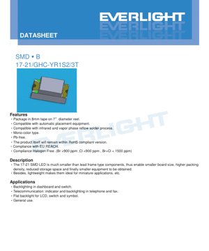
The 17-21/GHC-YR1S2/3T एक सतह-माउंट डिवाइस (SMD) LED है जो आधुनिक, कॉम्पैक्ट इलेक्ट्रॉनिक अनुप्रयोगों के लिए डिज़ाइन किया गया है। यह घटक पारंपरिक लीड-फ्रेम एलईडी की तुलना में एक महत्वपूर्ण प्रगति का प्रतिनिधित्व करता है, जो बोर्ड स्थान के उपयोग और असेंबली दक्षता के मामले में पर्याप्त लाभ प्रदान करता है।
1.1 उत्पाद स्थिति और मुख्य लाभ
यह LED एक मोनो-कलर प्रकार है, जो एक चमकदार हरी रोशनी उत्सर्जित करती है। इसका प्राथमिक लाभ इसके लघु आकार में निहित है। लीडेड घटकों की तुलना में काफी छोटा आकार डिजाइनरों को मुद्रित सर्किट बोर्ड (PCBs) पर उच्च पैकिंग घनत्व प्राप्त करने में सक्षम बनाता है। इसका सीधा परिणाम बोर्ड के आकार में कमी, घटकों के भंडारण की आवश्यकताओं में न्यूनीकरण और अंततः, छोटे और हल्के अंतिम-उपयोगकर्ता उपकरणों के निर्माण के रूप में होता है। पैकेज की हल्की प्रकृति इसे उन अनुप्रयोगों के लिए एक आदर्श विकल्प बनाती है जहां वजन एक महत्वपूर्ण कारक है।
1.2 लक्षित बाजार और अनुप्रयोग
यह उपकरण उपभोक्ता और औद्योगिक इलेक्ट्रॉनिक्स की एक विस्तृत श्रृंखला के लिए लक्षित है। इसके विशिष्ट अनुप्रयोगों में इंस्ट्रूमेंट पैनल, स्विच और प्रतीकों के लिए बैकलाइटिंग शामिल है। यह टेलीफोन और फैक्स मशीन जैसे उपकरणों के लिए स्टेटस संकेतक या बैकलाइट के रूप में दूरसंचार उपकरण में उपयोग के लिए भी उपयुक्त है। इसके अलावा, यह विभिन्न इलेक्ट्रॉनिक उत्पादों में एक सामान्य-उद्देश्य संकेतक प्रकाश के रूप में कार्य करता है।
2. तकनीकी मापदंडों का गहन विश्लेषण
यह खंड डेटाशीट में परिभाषित एलईडी के प्रमुख तकनीकी मापदंडों का विस्तृत, वस्तुनिष्ठ विश्लेषण प्रदान करता है।
2.1 Absolute Maximum Ratings
Absolute maximum ratings उन सीमाओं को परिभाषित करते हैं जिनके परे डिवाइस को स्थायी क्षति हो सकती है। ये संचालन की स्थितियाँ नहीं हैं।
- रिवर्स वोल्टेज (VR): 5V. यह ध्यान रखना महत्वपूर्ण है कि यह रेटिंग केवल इन्फ्रारेड (IR) परीक्षण स्थितियों के लिए निर्दिष्ट है। डेटाशीट स्पष्ट रूप से बताती है कि डिवाइस को वास्तविक सर्किट में रिवर्स संचालन के लिए डिज़ाइन नहीं किया गया है। रिवर्स बायस में इस वोल्टेज से अधिक होने पर तत्काल विफलता हो सकती है।
- फॉरवर्ड करंट (IF): 25 mA. यह एलईडी पर लगाया जा सकने वाला अधिकतम निरंतर डीसी करंट है।
- Peak Forward Current (IFP): 100 mA. यह अधिकतम पल्स करंट है, जो केवल 1 kHz पर 1/10 ड्यूटी साइकिल के तहत अनुमेय है। यह पैरामीटर मल्टीप्लेक्सिंग या PWM डिमिंग एप्लिकेशन के लिए प्रासंगिक है, लेकिन ओवरहीटिंग से बचने के लिए इसका उपयोग सावधानी से किया जाना चाहिए।
- Power Dissipation (Pd): 95 mW. यह पैकेज द्वारा व्यय की जा सकने वाली अधिकतम शक्ति है, जिसकी गणना अग्र वोल्टेज और धारा सीमाओं से की गई है, और यह तापीय प्रबंधन के लिए महत्वपूर्ण है।
- Operating & Storage Temperature: यह उपकरण -40°C से +85°C तक संचालित हो सकता है और -40°C से +90°C तक संग्रहीत किया जा सकता है। यह विस्तृत सीमा इसे कठोर वातावरण के लिए उपयुक्त बनाती है।
- सोल्डरिंग तापमान: रीफ्लो सोल्डरिंग के लिए, अधिकतम 10 सेकंड के लिए 260°C का शिखर तापमान निर्दिष्ट है। हैंड सोल्डरिंग के लिए, आयरन टिप का तापमान 350°C से अधिक नहीं होना चाहिए, और प्रति टर्मिनल संपर्क समय 3 सेकंड तक सीमित होना चाहिए।
2.2 इलेक्ट्रो-ऑप्टिकल विशेषताएँ
ये मापदंड 20 mA के फॉरवर्ड करंट (IF) और 25°C के परिवेश तापमान (Ta) की मानक परीक्षण स्थिति में मापे जाते हैं।
- Luminous Intensity (Iv): न्यूनतम 112.0 mcd से लेकर अधिकतम 285.0 mcd तक का परिसर है। विशिष्ट मान निर्दिष्ट नहीं है, जो दर्शाता है कि प्रदर्शन एक बिनिंग प्रणाली (विस्तार से बाद में) के माध्यम से प्रबंधित किया जाता है। सहनशीलता ±11% है।
- दृश्य कोण (2θ1/2): 140 डिग्री का एक विशिष्ट मान। यह चौड़ा दृश्य कोण LED को उन अनुप्रयोगों के लिए उपयुक्त बनाता है जिनमें व्यापक प्रकाश व्यवस्था या कई कोणों से दृश्यता की आवश्यकता होती है।
- शिखर तरंगदैर्ध्य (λp): आमतौर पर 518 nm, जो इसे दृश्यमान स्पेक्ट्रम के चमकीले हरे क्षेत्र में स्थापित करता है।
- प्रमुख तरंगदैर्ध्य (λd): 520.0 nm से 535.0 nm तक की सीमा में, ±1 nm की सख्त सहनशीलता के साथ। यह पैरामीटर प्रकाश के अनुभव किए गए रंग से अधिक निकटता से संबंधित है।
- स्पेक्ट्रल बैंडविड्थ (Δλ): आमतौर पर 35 nm, जो शिखर के आसपास उत्सर्जित प्रकाश की तरंगदैर्ध्य के प्रसार का वर्णन करता है।
- फॉरवर्ड वोल्टेज (VF): आमतौर पर 3.5V, 20 mA पर अधिकतम 4.0V। सर्किट डिजाइन के लिए यह एक महत्वपूर्ण पैरामीटर है, क्योंकि यह LED के पार वोल्टेज ड्रॉप और आवश्यक करंट-लिमिटिंग रेसिस्टर मान निर्धारित करता है।
- रिवर्स करंट (IR): 5V रिवर्स वोल्टेज पर अधिकतम 50 μA (टेस्ट कंडीशन)।
3. बिनिंग सिस्टम व्याख्या
सुसंगत प्रदर्शन सुनिश्चित करने के लिए, एलईडी को प्रमुख प्रकाशिक मापदंडों के आधार पर बिन में वर्गीकृत किया जाता है। यह डिजाइनरों को विशिष्ट चमक और रंग आवश्यकताओं को पूरा करने वाले भागों का चयन करने की अनुमति देता है।
3.1 Luminous Intensity Binning
एलईडी को 20 एमए पर मापी गई उनकी चमकदार तीव्रता के आधार पर चार श्रेणियों (आर1, आर2, एस1, एस2) में वर्गीकृत किया गया है।
- श्रेणी आर1: 112.0 – 140.0 mcd
- Bin R2: 140.0 – 180.0 mcd
- Bin S1: 180.0 – 225.0 mcd
- Bin S2: 225.0 – 285.0 mcd
The selection of a higher bin (e.g., S2) guarantees higher minimum brightness, which is essential for applications requiring high visibility or where multiple LEDs need to be matched for uniform appearance.
3.2 Dominant Wavelength Binning
रंग स्थिरता नियंत्रित करने के लिए एलईडी को उनकी प्रमुख तरंगदैर्ध्य के आधार पर तीन समूहों (X, Y, Z) में भी वर्गीकृत किया जाता है।
- Bin X: 520.0 – 525.0 nm
- Bin Y: 525.0 – 530.0 nm
- Bin Z: 530.0 – 535.0 nm
For applications where color matching between multiple LEDs is critical (e.g., status bars, backlight arrays), specifying a single, narrow bin is necessary to avoid visible color differences.
4. यांत्रिक और पैकेज सूचना
4.1 पैकेज आयाम
17-21 SMD LED का एक कॉम्पैक्ट आयताकार पैकेज होता है। मुख्य आयामों में 1.6 मिमी लंबाई, 0.8 मिमी चौड़ाई और 0.6 मिमी ऊंचाई शामिल है (सहनशीलता ±0.1 मिमी जब तक अन्यथा नोट न किया गया हो)। डेटाशीट में पैड लेआउट सहित एक विस्तृत आयामी चित्र प्रदान किया गया है, जो PCB फुटप्रिंट बनाने के लिए आवश्यक है। सही पैड डिजाइन उचित सोल्डरिंग, संरेखण और थर्मल प्रदर्शन सुनिश्चित करता है।
4.2 ध्रुवीयता पहचान
कैथोड को आमतौर पर पैकेज पर एक चिह्न या एक विशिष्ट पैड ज्यामिति (जैसे, एक चैम्फर्ड कोना) द्वारा पहचाना जाता है। प्लेसमेंट के दौरान सही पोलैरिटी ओरिएंटेशन सर्किट के कार्य करने के लिए महत्वपूर्ण है।
5. Soldering and Assembly Guide
एसएमडी एलईडी की विश्वसनीयता और प्रदर्शन के लिए उचित हैंडलिंग और सोल्डरिंग महत्वपूर्ण है।
5.1 Reflow Soldering Profile
The datasheet specifies a lead-free reflow soldering profile. Key phases include:
- प्री-हीटिंग: 60-120 सेकंड में परिवेशी तापमान से 150-200°C तक रैंप करें।
- सोक/रीफ्लो: लिक्विडस (217°C) से ऊपर का समय 60-150 सेकंड होना चाहिए। शीर्ष तापमान 260°C से अधिक नहीं होना चाहिए, और 255°C या उससे ऊपर का समय अधिकतम 30 सेकंड तक सीमित होना चाहिए।
- शीतलन: अधिकतम शीतलन दर 6°C प्रति सेकंड से अधिक नहीं होनी चाहिए।
महत्वपूर्ण नोट: एक ही एलईडी असेंबली पर रीफ्लो सोल्डरिंग दो बार से अधिक नहीं की जानी चाहिए ताकि पैकेज और डाई को थर्मल क्षति से बचाया जा सके।
5.2 भंडारण और नमी संवेदनशीलता
यह घटक नमी-संवेदनशील है। सावधानियों में शामिल हैं:
- जब तक घटक उपयोग के लिए तैयार न हों, तब तक नमी-रोधी बैरियर बैग न खोलें।
- खोलने के बाद, अनुपयोगी LEDs को ≤30°C और ≤60% सापेक्ष आर्द्रता पर संग्रहित किया जाना चाहिए।
- बैग खोलने के बाद "फ्लोर लाइफ" 168 घंटे (7 दिन) है। यदि इस समय के भीतर उपयोग नहीं किया जाता है, तो उपयोग से पहले LEDs को 60 ±5°C पर 24 घंटे के लिए पुनः बेक किया जाना चाहिए।
- यदि डिसिकेंट इंडिकेटर का रंग बदल गया है, तो समय की परवाह किए बिना बेकिंग आवश्यक है।
5.3 हाथ से सोल्डरिंग और पुनर्कार्य
यदि हाथ से सोल्डरिंग अपरिहार्य है, तो अत्यधिक सावधानी बरतनी चाहिए:
- सोल्डरिंग आयरन टिप का तापमान ≤350°C होना चाहिए।
- प्रत्येक टर्मिनल पर संपर्क समय ≤3 सेकंड होना चाहिए, प्रत्येक टर्मिनल की सोल्डरिंग के बीच कम से कम 2 सेकंड का अंतराल ठंडा होने के लिए देना चाहिए।
- सोल्डरिंग के बाद मरम्मत की दृढ़ता से हतोत्साहित किया जाता है। यदि बिल्कुल आवश्यक हो, तो दोनों टर्मिनलों को एक साथ गर्म करने के लिए दोहरे सिरे वाले सोल्डरिंग आयरन का उपयोग किया जाना चाहिए, ताकि थर्मल स्ट्रेस कम से कम हो। LED विशेषताओं पर प्रभाव की पूर्व जांच आवश्यक है।
6. पैकेजिंग और आर्डर जानकारी
6.1 मानक पैकेजिंग
एलईडी को नमी-प्रतिरोधी पैकेजिंग में आपूर्ति की जाती है, जिसमें शामिल हैं:
- 8mm चौड़ी वाहक टेप में रखे गए घटक।
- The tape is wound on a 7-inch diameter reel.
- A standard reel contains 3000 pieces.
- रील को एक एल्यूमीनियम नमी-रोधी बैग के अंदर रखा जाता है, जिसमें एक सिलिका जेल पैकेट और एक आर्द्रता संकेतक कार्ड होता है।
6.2 लेबल स्पष्टीकरण
रील लेबल में कोड होते हैं जो उस रील पर लगे एलईडी की सटीक विशेषताओं को निर्दिष्ट करते हैं:
- P/N: Product Number (e.g., 17-21/GHC-YR1S2/3T).
- CAT: चमकदार तीव्रता रैंक (बिन कोड से संबंधित: R1, R2, S1, S2).
- HUE: Chromaticity Coordinates & Dominant Wavelength Rank (corresponds to the bin code: X, Y, Z).
- संदर्भ: फॉरवर्ड वोल्टेज रैंक.
- LOT No: ट्रेस करने योग्य निर्माण लॉट नंबर।
7. अनुप्रयोग सुझाव और डिज़ाइन विचार
7.1 करंट लिमिटिंग अनिवार्य है
एक बाहरी करंट-लिमिटिंग रेसिस्टर नितांत आवश्यक है। एलईडी करंट-संचालित उपकरण हैं। फॉरवर्ड वोल्टेज में एक छोटी सी वृद्धि फॉरवर्ड करंट में एक बड़ी, संभावित रूप से विनाशकारी वृद्धि का कारण बन सकती है। रेसिस्टर मान (R) की गणना ओम के नियम का उपयोग करके की जा सकती है: R = (V_supply - VF_LED) / I_desired। हमेशा *टिपिकल* VF के लिए डिज़ाइन करें ताकि यह सुनिश्चित हो सके कि यदि वास्तविक VF निर्दिष्ट न्यूनतम मान पर है तो करंट सीमा के भीतर रहे।
7.2 थर्मल मैनेजमेंट
छोटा होने के बावजूद, एलईडी ऊष्मा उत्पन्न करती है। 95 mW पावर डिसिपेशन सीमा का पालन किया जाना चाहिए। सुनिश्चित करें कि पीसीबी पैड डिज़ाइन पर्याप्त थर्मल रिलीफ प्रदान करता है, खासकर यदि अधिकतम निरंतर करंट (25 mA) पर या उसके निकट संचालित किया जा रहा हो। एलईडी को अन्य ऊष्मा उत्पन्न करने वाले घटकों के पास रखने से बचें।
7.3 ESD सावधानियाँ
डिवाइस की ESD रेटिंग 1000V (ह्यूमन बॉडी मॉडल) है। असेंबली और हैंडलिंग के दौरान मानक ESD हैंडलिंग प्रक्रियाओं का पालन किया जाना चाहिए ताकि अव्यक्त क्षति को रोका जा सके, जो तत्काल विफलता का कारण नहीं बन सकती है लेकिन दीर्घकालिक विश्वसनीयता को कम कर सकती है।
8. तकनीकी तुलना और विभेदन
17-21 LED की प्राथमिक विशिष्टता इसके फॉर्म फैक्टर और प्रदर्शन संतुलन में निहित है।
- vs. Larger SMD LEDs (e.g., 3528, 5050): यह काफी छोटा फुटप्रिंट प्रदान करता है, जो उच्च-घनत्व डिज़ाइन सक्षम करता है, लेकिन आमतौर पर प्रति डिवाइस कुल प्रकाश उत्पादन कम होता है।
- बनाम चिप-स्केल पैकेज (सीएसपी): यह अत्याधुनिक सीएसपी एलईडी से बड़ा है, लेकिन मानक एसएमटी उपकरणों से संभालना आसान है और कई अनुप्रयोगों के लिए एक अधिक मजबूत पैकेज प्रदान करता है।
- बनाम लीडेड एलईडी: यह थ्रू-होल्स की आवश्यकता को समाप्त करता है, स्वचालित पिक-एंड-प्लेस असेंबली को सक्षम बनाता है, परजीवी प्रेरकत्व को कम करता है, और बहुत छोटे और हल्के अंतिम उत्पादों की अनुमति देता है।
9. अक्सर पूछे जाने वाले प्रश्न (तकनीकी मापदंडों के आधार पर)
9.1 क्या मैं इस LED को करंट-लिमिटिंग रेसिस्टर के बिना चला सकता हूँ?
नहीं। "उपयोग के लिए सावधानियाँ" खंड में इसके विरुद्ध स्पष्ट चेतावनी दी गई है। फॉरवर्ड वोल्टेज की एक सीमा होती है (सामान्यतः 3.5V, अधिकतम 4.0V)। इसे सीधे एक वोल्टेज स्रोत से जोड़ना, भले ही वह इसके VF से थोड़ा ही अधिक हो, अत्यधिक करंट का कारण बनेगा, जिससे तेजी से अधिक गर्मी होगी और यह खराब हो जाएगा। सुरक्षित संचालन के लिए एक श्रृंखला रेसिस्टर अनिवार्य है।
9.2 रिवर्स वोल्टेज रेटिंग केवल 5V क्यों है, और नोट का क्या अर्थ है?
5V रेटिंग केवल रिवर्स लीकेज करंट (IR) मापने के परीक्षण उद्देश्यों के लिए है। डेटाशीट स्पष्ट रूप से कहती है "The device is not designed for reverse operation." एक सर्किट में, आपको यह सुनिश्चित करना चाहिए कि LED कभी भी रिवर्स बायस के अधीन न हो, क्योंकि यह एक जेनर डायोड नहीं है और यदि रिवर्स-बायस्ड किया जाता है तो 5V से काफी नीचे वोल्टेज पर भी क्षतिग्रस्त होने की संभावना है। उन सर्किटों में सुरक्षा डायोड का उपयोग करें जहां रिवर्स वोल्टेज संभव है (जैसे, AC coupling, inductive loads).
9.3 मैं सही बिन कोड कैसे चुनूं?
अपने एप्लिकेशन की आवश्यकताओं के आधार पर बिन का चयन करें:
10. डिज़ाइन और उपयोग केस स्टडी
10.1 एक कॉम्पैक्ट स्टेटस इंडिकेटर पैनल डिज़ाइन करना
परिदृश्य: एक नेटवर्किंग डिवाइस के लिए 20 स्टेटस इंडिकेटर्स का एक घना पैनल डिजाइन करना। यूजर अनुभव के लिए एकसमान चमक और रंग महत्वपूर्ण हैं। डिज़ाइन चरण: 1. वर्तमान सेटिंग: अच्छी चमक और लंबी उम्र के लिए 15 mA (25 mA अधिकतम से कम) की ड्राइव धारा चुनें। 5V आपूर्ति के लिए प्रतिरोधक मान की गणना करें: R = (5V - 3.5V) / 0.015A = 100 ओम। 1% सहनशीलता वाला प्रतिरोधक उपयोग करें। बिनिंग चयन: एकरूपता सुनिश्चित करने के लिए, सभी एलईडी एक ही चमकदार तीव्रता बिन (जैसे, S1) और एक ही प्रमुख तरंगदैर्ध्य बिन (जैसे, Y) से निर्दिष्ट करें। ऑर्डर करते समय यह जानकारी प्रदान की जानी चाहिए। पीसीबी लेआउट: डेटाशीट से पैड के सटीक आयामों का उपयोग करें। सोल्डरिंग में सहायता और टॉम्बस्टोनिंग को रोकने के लिए प्रत्येक पैड के लिए एक छोटा थर्मल रिलीफ कनेक्शन प्रदान करें, लेकिन यह सुनिश्चित करें कि तांबे का क्षेत्र हीट डिसिपेशन के लिए पर्याप्त है। असेंबली: निर्दिष्ट रीफ्लो प्रोफाइल का पालन करें। 7-दिन के फ्लोर लाइफ का सम्मान करने के लिए, पैनलों को सीलबंद बैग में तब तक रखें जब तक उन्हें पिक-एंड-प्लेस मशीन में लोड नहीं किया जाता।
11. Operating Principle Introduction
17-21/GHC-YR1S2/3T LED, डिवाइस चयन गाइड के अनुसार, इंडियम गैलियम नाइट्राइड (InGaN) से बने एक सेमीकंडक्टर चिप पर आधारित है। जब डायोड के अंतर्निहित विभव से अधिक का फॉरवर्ड वोल्टेज लगाया जाता है, तो इलेक्ट्रॉन और होल सेमीकंडक्टर के सक्रिय क्षेत्र में इंजेक्ट होते हैं। उनके पुनर्संयोजन से फोटॉन (प्रकाश) के रूप में ऊर्जा मुक्त होती है। InGaN सामग्री की विशिष्ट संरचना बैंडगैप ऊर्जा निर्धारित करती है, जो सीधे उत्सर्जित प्रकाश की तरंगदैर्ध्य (रंग) से संबंधित होती है—इस मामले में, चमकदार हरा (~518 nm पीक)। वाटर-क्लियर रेजिन एनकैप्सुलेंट चिप की सुरक्षा करता है और एक लेंस के रूप में कार्य करते हुए, उत्सर्जित प्रकाश के 140-डिग्री व्यूइंग एंगल को आकार देता है।
12. Technology Trends and Context
17-21 पैकेज SMD LED बाजार में एक परिपक्व और व्यापक रूप से अपनाई गई फॉर्म फैक्टर का प्रतिनिधित्व करता है। LED प्रौद्योगिकी का सामान्य रुझान ऐसे घटकों से संबंधित कई प्रमुख क्षेत्रों की ओर बना हुआ है:
- बढ़ी हुई दक्षता: सामग्री विज्ञान में निरंतर सुधार का लक्ष्य प्रति वाट अधिक लुमेन (उच्च दक्षता) उत्पन्न करना है, जिसका अर्थ है समान आकार के पैकेज के लिए चमकदार प्रकाश या कम बिजली की खपत।
- लघुरूपण: हालांकि 17-21 (1.6x0.8mm) आकार में छोटा है, उद्योग और भी छोटे चिप-स्केल पैकेज (CSP) की ओर बढ़ रहा है जो लगभग नग्न सेमीकंडक्टर डाई के आकार के होते हैं, जिससे अति-उच्च-घनत्व प्रकाश व्यवस्था सरणियाँ संभव होती हैं।
- बेहतर रंग स्थिरता: एपिटैक्सियल विकास और बिनिंग प्रक्रियाओं में प्रगति से प्रमुख तरंगदैर्ध्य और दीप्त तीव्रता पर सख्त नियंत्रण संभव हुआ है, जिससे कुछ अनुप्रयोगों में कठोर बिन चयन की आवश्यकता कम हो गई है।
- बढ़ी हुई विश्वसनीयता: पैकेजिंग सामग्रियों में सुधार, जैसे कि अधिक मजबूत सिलिकोन और फॉस्फर (सफेद एलईडी के लिए), और बेहतर थर्मल प्रबंधन डिजाइन, संचालन जीवनकाल को बढ़ाते हैं और उच्च-तापमान वाले वातावरण में उपयोग की अनुमति देते हैं।
यह डेटाशीट एक विश्वसनीय, अच्छी तरह से चरित्रित घटक को दर्शाती है जो मुख्यधारा के इलेक्ट्रॉनिक अनुप्रयोगों की एक विस्तृत श्रृंखला के लिए प्रदर्शन, आकार और निर्माण क्षमता के बीच संतुलन बनाती है।
LED Specification Terminology
LED तकनीकी शब्दों की पूर्ण व्याख्या
प्रकाशविद्युत प्रदर्शन
| शब्द | इकाई/प्रतिनिधित्व | सरल व्याख्या | महत्वपूर्ण क्यों |
|---|---|---|---|
| दीप्त प्रभावकारिता | lm/W (लुमेन प्रति वाट) | प्रति वाट बिजली से प्रकाश उत्पादन, अधिक होने का अर्थ है अधिक ऊर्जा कुशल। | सीधे ऊर्जा दक्षता ग्रेड और बिजली लागत निर्धारित करता है। |
| Luminous Flux | lm (लुमेन) | स्रोत द्वारा उत्सर्जित कुल प्रकाश, जिसे आमतौर पर "चमक" कहा जाता है। | प्रकाश पर्याप्त चमकीला है या नहीं, यह निर्धारित करता है। |
| Viewing Angle | ° (degrees), e.g., 120° | वह कोण जहाँ प्रकाश की तीव्रता आधी रह जाती है, यह बीम की चौड़ाई निर्धारित करता है। | प्रकाशन सीमा और एकरूपता को प्रभावित करता है। |
| CCT (रंग तापमान) | K (केल्विन), उदाहरणार्थ, 2700K/6500K | प्रकाश की गर्माहट/ठंडक, कम मान पीलेपन/गर्माहट, अधिक मान सफेदी/ठंडक दर्शाते हैं। | प्रकाश व्यवस्था का वातावरण और उपयुक्त परिदृश्य निर्धारित करता है। |
| CRI / Ra | इकाईहीन, 0–100 | वस्तुओं के रंगों को सटीकता से प्रस्तुत करने की क्षमता, Ra≥80 अच्छा माना जाता है। | रंग की प्रामाणिकता को प्रभावित करता है, मॉल, संग्रहालय जैसे उच्च मांग वाले स्थानों में प्रयुक्त। |
| SDCM | मैकएडम दीर्घवृत्त चरण, उदाहरण के लिए, "5-चरण" | रंग स्थिरता मापदंड, छोटे चरण अधिक सुसंगत रंग का संकेत देते हैं। | एलईडी के समान बैच में एकसमान रंग सुनिश्चित करता है। |
| Dominant Wavelength | nm (नैनोमीटर), उदाहरणार्थ, 620nm (लाल) | रंगीन एलईडी के रंग के अनुरूप तरंगदैर्ध्य। | लाल, पीले, हरे मोनोक्रोम LED के रंग का स्वर निर्धारित करता है। |
| Spectral Distribution | Wavelength vs intensity curve | Shows intensity distribution across wavelengths. | Affects color rendering and quality. |
विद्युत मापदंड
| शब्द | प्रतीक | सरल व्याख्या | डिज़ाइन संबंधी विचार |
|---|---|---|---|
| अग्र वोल्टेज | Vf | एलईडी चालू करने के लिए न्यूनतम वोल्टेज, जैसे "प्रारंभिक सीमा"। | ड्राइवर वोल्टेज ≥Vf होना चाहिए, श्रृंखला में जुड़े एलईडी के लिए वोल्टेज जुड़ते हैं। |
| Forward Current | If | Current value for normal LED operation. | Usually constant current drive, current determines brightness & lifespan. |
| अधिकतम पल्स धारा | Ifp | कम समय के लिए सहन करने योग्य शिखर धारा, मंद या चमक के लिए उपयोग की जाती है। | Pulse width & duty cycle must be strictly controlled to avoid damage. |
| Reverse Voltage | Vr | Max reverse voltage LED can withstand, beyond may cause breakdown. | सर्किट को रिवर्स कनेक्शन या वोल्टेज स्पाइक्स को रोकना चाहिए। |
| Thermal Resistance | Rth (°C/W) | चिप से सोल्डर तक ऊष्मा स्थानांतरण के लिए प्रतिरोध, कम होना बेहतर है। | उच्च तापीय प्रतिरोध के लिए मजबूत ऊष्मा अपव्यय की आवश्यकता होती है। |
| ESD Immunity | V (HBM), e.g., 1000V | इलेक्ट्रोस्टैटिक डिस्चार्ज को सहन करने की क्षमता, उच्च मान का अर्थ है कम संवेदनशीलता। | उत्पादन में एंटी-स्टैटिक उपायों की आवश्यकता, विशेष रूप से संवेदनशील एलईडी के लिए। |
Thermal Management & Reliability
| शब्द | प्रमुख मापदंड | सरल व्याख्या | प्रभाव |
|---|---|---|---|
| जंक्शन तापमान | Tj (°C) | एलईडी चिप के अंदर का वास्तविक कार्यशील तापमान। | हर 10°C कमी जीवनकाल को दोगुना कर सकती है; बहुत अधिक तापमान प्रकाश क्षय, रंग परिवर्तन का कारण बनता है। |
| Lumen Depreciation | L70 / L80 (घंटे) | प्रारंभिक चमक के 70% या 80% तक गिरने में लगा समय। | सीधे तौर पर LED की "सेवा जीवन" को परिभाषित करता है। |
| लुमेन रखरखाव | % (उदाहरण के लिए, 70%) | समय के बाद बची हुई चमक का प्रतिशत। | दीर्घकालिक उपयोग में चमक की स्थिरता को दर्शाता है। |
| Color Shift | Δu′v′ या मैकएडम दीर्घवृत्त | उपयोग के दौरान रंग परिवर्तन की डिग्री। | प्रकाश दृश्यों में रंग स्थिरता को प्रभावित करता है। |
| Thermal Aging | सामग्री अवक्रमण | दीर्घकालिक उच्च तापमान के कारण ह्रास। | इससे चमक में कमी, रंग परिवर्तन, या ओपन-सर्किट विफलता हो सकती है। |
Packaging & Materials
| शब्द | सामान्य प्रकार | सरल व्याख्या | Features & Applications |
|---|---|---|---|
| पैकेज प्रकार | EMC, PPA, Ceramic | हाउसिंग सामग्री चिप की सुरक्षा करती है, ऑप्टिकल/थर्मल इंटरफेस प्रदान करती है। | EMC: अच्छी हीट रेजिस्टेंस, कम लागत; Ceramic: बेहतर हीट डिसिपेशन, लंबी लाइफ। |
| Chip Structure | फ्रंट, फ्लिप चिप | चिप इलेक्ट्रोड व्यवस्था। | फ्लिप चिप: बेहतर ताप अपव्यय, उच्च प्रभावकारिता, उच्च-शक्ति के लिए। |
| फॉस्फर कोटिंग | YAG, Silicate, Nitride | नीले चिप को कवर करता है, कुछ को पीले/लाल में परिवर्तित करता है, सफेद में मिलाता है। | विभिन्न फॉस्फर प्रभावकारिता, CCT, और CRI को प्रभावित करते हैं। |
| लेंस/ऑप्टिक्स | फ्लैट, माइक्रोलेंस, TIR | सतह पर प्रकाश वितरण को नियंत्रित करने वाली प्रकाशीय संरचना। | दृश्य कोण और प्रकाश वितरण वक्र निर्धारित करता है। |
Quality Control & Binning
| शब्द | बिनिंग कंटेंट | सरल व्याख्या | उद्देश्य |
|---|---|---|---|
| Luminous Flux Bin | कोड उदाहरण के लिए, 2G, 2H | चमक के आधार पर समूहीकृत, प्रत्येक समूह के न्यूनतम/अधिकतम लुमेन मान होते हैं। | एक ही बैच में समान चमक सुनिश्चित करता है। |
| Voltage Bin | Code e.g., 6W, 6X | Forward voltage range ke anusaar vargikrit. | Driver matching ko sahaj banata hai, system efficiency ko sudhaarta hai. |
| Color Bin | 5-step MacAdam ellipse | रंग निर्देशांकों के आधार पर समूहीकृत, सुनिश्चित करता है कि सीमा सघन हो। | रंग स्थिरता की गारंटी देता है, फिक्स्चर के भीतर असमान रंग से बचाता है। |
| CCT Bin | 2700K, 3000K आदि। | CCT के अनुसार समूहीकृत, प्रत्येक की एक संगत निर्देशांक सीमा होती है। | विभिन्न दृश्य CCT आवश्यकताओं को पूरा करता है। |
Testing & Certification
| शब्द | Standard/Test | सरल व्याख्या | महत्त्व |
|---|---|---|---|
| LM-80 | लुमेन रखरखाव परीक्षण | निरंतर तापमान पर दीर्घकालिक प्रकाश व्यवस्था, चमक क्षय रिकॉर्ड करना। | LED जीवन का अनुमान लगाने के लिए उपयोग किया जाता है (TM-21 के साथ)। |
| TM-21 | जीवन अनुमान मानक | LM-80 डेटा के आधार पर वास्तविक परिस्थितियों में जीवन का अनुमान लगाता है। | वैज्ञानिक जीवन पूर्वानुमान प्रदान करता है। |
| IESNA | Illuminating Engineering Society | प्रकाशिक, विद्युत, तापीय परीक्षण विधियों को शामिल करता है। | उद्योग-मान्यता प्राप्त परीक्षण आधार। |
| RoHS / REACH | पर्यावरण प्रमाणन | यह सुनिश्चित करता है कि कोई हानिकारक पदार्थ (सीसा, पारा) न हों। | अंतरराष्ट्रीय स्तर पर बाजार पहुंच आवश्यकता। |
| ENERGY STAR / DLC | ऊर्जा दक्षता प्रमाणन | प्रकाश व्यवस्था के लिए ऊर्जा दक्षता और प्रदर्शन प्रमाणन। | सरकारी खरीद, सब्सिडी कार्यक्रमों में प्रयुक्त, प्रतिस्पर्धात्मकता बढ़ाता है। |