목차
1. 제품 개요
EL111X-G 시리즈는 광트랜지스터 기반의 광커플러(광결합기)로, 서로 다른 전위를 가진 회로 간에 신뢰할 수 있는 전기적 절연과 신호 전송이 필요한 애플리케이션을 위해 설계되었습니다. 이 소자의 핵심 기능은 빛을 이용해 전기 신호를 전송하여 입력측(적외선 발광 다이오드)과 출력측(광트랜지스터 검출기) 사이에 전기적 절연을 제공하는 것입니다. 이러한 절연은 고전압, 노이즈 및 접지 루프로부터 민감한 회로를 보호하는 데 매우 중요합니다.
该系列的特点是采用紧凑的5引脚小外形封装(SOP),高度仅为2.0毫米,适合空间受限的PCB设计。一个关键的区分特征是8毫米的长爬电距离,通过增加沿封装体表面的导电部件之间的距离,提高了高压环境下的可靠性和安全性。器件采用不含卤素(溴<900 ppm,氯<900 ppm,Br+Cl<1500 ppm)和三氧化二锑(Sb2O3)的复合材料制造,符合环境和安全法规。
2. 기술 사양 상세 설명
2.1 절대 최대 정격
이 정격값들은 소자에 영구적인 손상을 초래할 수 있는 한계를 정의합니다. 이러한 조건에서 동작할 경우 성능이 보장되지 않습니다.
- 입력 순방향 전류(IF):60 mA (연속). 1µs 펄스의 경우, 피크 순방향 전류는 스위칭 시 짧은 과전류를 허용하기 위해 1.5 A로 훨씬 더 높습니다.
- 입력 역전압(VR):6 V. 역방향 바이어스에서 이 전압을 초과하면 입력 LED가 손상될 수 있습니다.
- 출력 컬렉터-이미터 전압(VCEO):80 V. 이는 베이스가 개방되었을 때 출력 트랜지스터 양단에 인가할 수 있는 최대 전압입니다.
- 출력 컬렉터 전류(IC):50 mA.
- 총 소비 전력(PTOT):250 mW. 이는 입력 및 출력 양측의 최대 총 소비 전력입니다.
- 절연 전압(VISO):5000 Vrms(40-60% 상대 습도에서 1분간 유지). 이는 핵심 안전 파라미터로, 테스트 시 입력 핀(1,2)을 함께 단락시키고 출력 핀(3,4,5)을 함께 단락시킵니다.
- 동작 온도 (TOPR):-55°C ~ +110°C.
- 솔더링 온도 (TSOL):260°C에서 10초간 유지, 일반적인 리플로우 솔더링 온도 프로파일 준수.
2.2 광전 특성
이 매개변수들은 정상 작동 조건에서의 소자 성능을 정의합니다 (별도 명시되지 않는 한, Ta=25°C).
2.2.1 입력 특성 (적외선 LED)
- 순방향 전압(VF):IF = 50 mA일 때, 최대값은 1.5 V입니다. 일반적인 값은 더 낮으며, 대략 1.1-1.3V 정도입니다.
- 역방향 전류(IR):VR = 6 V일 때, 최대값은 10 µA입니다.
- 입력 커패시턴스 (Cin):1 kHz에서 전형적인 값은 50 pF입니다. 이는 고주파 스위칭 성능에 영향을 미칩니다.
2.2.2 출력 특성 (포토트랜지스터)
- 컬렉터-이미터 암전류 (ICEO):V에서CE= 20V, IF= 0mA일 때, 최대값은 100 nA입니다. 이는 LED가 꺼져 있을 때의 누설 전류입니다.
- 콜렉터-이미터 항복 전압 (BVCEO):IC= 0.1mA일 때, 최소값은 80 V입니다.
- 콜렉터-이미터 포화 전압 (VCE(sat)):IF= 10mA, IC= 1mA일 때, 최대값은 0.4V입니다. 논리 레벨 입력을 구동하는 출력 단의 경우, 낮은 포화 전압이 바람직합니다.
2.2.3 전달 특성
이 매개변수들은 입력과 출력 간의 결합 효율과 속도를 설명합니다.
- 전류 전송비(CTR):이는 출력 컬렉터 전류(IC)와 입력 순방향 전류(IF)의 비율을 백분율로 나타낸 것입니다. EL111X-G 시리즈는 다양한 CTR 등급을 제공하며, 각 등급은 지정된 테스트 조건에서 명시된 최소/최대 범위를 가집니다. 이를 통해 설계자는 일관된 이득을 가진 소자를 자신의 애플리케이션에 맞게 선택할 수 있습니다.
- EL1110, EL1116, EL1117, EL1118, EL1119:IF= 5mA, VCE= 5V 조건에서 테스트. 범위는 50-600%(EL1110)에서 200-400%(EL1119)까지 다양함.
- EL1112, EL1113, EL1114:IF= 10mA, VCE= 5V 조건에서 테스트. 범위는 각각 63-125%, 100-200% 및 160-320%입니다. 이 소자들은 IF= 1mA에서도 지정된 최소 CTR 값을 가집니다.
- 절연 저항 (RIO):500V DC에서 최소값은 5 x 10¹⁰Ω입니다. 이는 절연 측 사이의 DC 저항이 매우 높음을 나타냅니다.
- 부유 커패시턴스(CIO):1 MHz에서 최대값은 1.0 pF입니다. 이 낮은 커패시턴스는 노이즈의 용량성 결합을 최소화하여 높은 공통 모드 과도 내성(CMTI)을 유지하는 데 기여합니다.
- 스위칭 시간:V에서CE= 5V, IC= 5mA, RL= 100Ω 조건에서 측정.
- 켜짐 시간 (ton):전형값 4 µs.
- 차단 시간 (toff):전형값 3 µs.
- 상승 시간 (tr):전형값 2 µs, 최대값 18 µs.
- 하강 시간 (tf):전형값 3 µs, 최대값 18 µs.
3. 등급 시스템 설명
EL111X-G 시리즈의 주요 등급 시스템은전류 전달비(CTR). 서로 다른 부품 번호(EL111X의 'X'로 표시)는 표준 조건(IF=5mA 또는 10mA, VCE=5V)로 측정된 특정하고 보장된 CTR 범위입니다. 이를 통해 설계자는 다음과 같은 작업을 할 수 있습니다:
- 회로 안정성 확보:더 좁은 CTR 범위(예: EL1117: 80-160%)를 선택하면 주어진 입력 전류에 대해 더 예측 가능한 출력 전류를 제공하여 광범위 허용 오차 바이어스 회로의 필요성을 줄일 수 있습니다.
- 전력 소모 최적화:원하는 출력 전류의 경우, 더 높은 CTR 소자(예: EL1119)를 더 낮은 입력 LED 전류로 구동하여 일차측 전력을 절약할 수 있습니다.
- 설계 요구사항 맞춤:다양한 응용 분야는 서로 다른 이득을 필요로 할 수 있습니다. 논리 인터페이스 회로는 표준 CTR 소자를 사용할 수 있는 반면, 아날로그 신호 전송은 더 높고 선형적인 CTR 소자를 사용함으로써 이점을 얻을 수 있습니다.
주문 정보는 'X' 문자(0, 2, 3, 4, 6, 7, 8, 9)를 통해 이러한 등급을 명확히 정의합니다.
4. 성능 곡선 분석
데이터시트에 구체적인 그래프 곡선("전형적인 광전 특성 곡선")이 인용되어 있지만, 광전 트랜지스터 광커플러의 원리에 따라 전형적인 동작을 설명할 수 있습니다:
- CTR과 순방향 전류(IF)의 관계:CTR는 일정하지 않습니다. 일반적으로 중간 수준의 순방향 전류(이러한 소자의 경우 보통 5-10mA 정도)에서 최고치에 도달하며, 매우 낮거나 매우 높은 전류에서는 LED 효율과 트랜지스터 포화 효과로 인해 감소할 수 있습니다.
- CTR과 온도의 관계:CTR은 일반적으로 음의 온도 계수를 갖습니다; 접합 온도가 상승함에 따라 감소합니다. 설계자는 전체 작동 온도 범위에서 이러한 감액을 고려해야 합니다.
- 출력 전류(IC)와 콜렉터-에미터 전압(VCE)의 관계:고정된 LED 전류에 대해, 포토트랜지스터는 포화 상태에 진입할 때까지 전류원과 유사하게 동작합니다. 포화 영역은 낮은 VCE(sat)을 특징으로 하며, 사양에 표시된 바와 같습니다.
- 스위칭 시간과 부하 저항(RL)의 관계:스위칭 시간(tr, tf)은 부하 저항과 기생 커패시턴스에 크게 의존합니다. 더 작은 RL은 일반적으로 더 빠른 하강 시간을 제공하지만, 출력 스윙을 감소시키고 전력 소비를 증가시킵니다.
5. 기계 및 패키징 정보
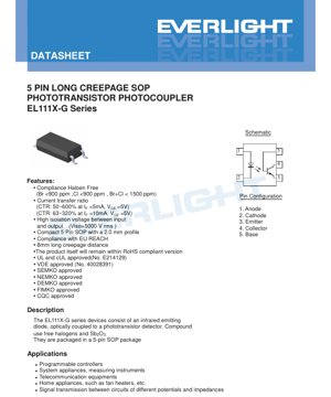
해당 소자는 높이 2.0mm의 5핀 SOP(소형 패키지)를 채용합니다. 핀 구성은 표준화되어 있습니다:
- 애노드(입력 LED+)
- 캐소드(입력 LED-)
- 이미터(포토트랜지스터)
- 콜렉터(포토트랜지스터)
- 베이스(포토트랜지스터, 일반적으로 개방 또는 가속 기술에 연결)
패키지는 하나를 포함합니다권장 패드 레이아웃, 표면 실장 어셈블리를 위한 것으로, 리플로우 솔더링 과정에서 신뢰할 수 있는 솔더 접합과 적절한 기계적 안정성을 확보하는 데 중요합니다.8mm 길이 크리프이지 거리이는 패키지 몰드의 물리적 설계 특징으로, 입력 및 출력 핀 간의 표면 거리를 증가시켜 5000Vrms의 높은 절연 정격을 달성하고 안전 표준을 준수하는 데 직접적으로 기여합니다.
6. 용접 및 조립 가이드
해당 소자의 최고 솔더링 온도 정격은 260°C에서 10초 동안 유지입니다. 이는 표준 무연 리플로우 솔더링 온도 프로파일(IPC/JEDEC J-STD-020)을 준수합니다. 주요 주의사항은 다음과 같습니다:
- 권장 PCB 패드 패턴을 사용하여 툼스토닝(tombstoning) 또는 오정렬을 방지하십시오.
- 과도한 솔더 페이스트 사용을 피하십시오. 이는 리드 간 브리징(bridging) 또는 크리피지 거리(creepage distance) 단락을 초래할 수 있습니다.
- 플라스틱 패키지의 표준 Moisture Sensitivity Level(MSL) 처리 절차를 따르십시오. 부품이 지정된 저장 수명 이상의 환경 습도에 노출된 경우, 일반적으로 베이킹(baking)이 필요합니다.
- 저장 온도 범위는 -55°C ~ +125°C입니다.
7. 포장 및 주문 정보
이 제품은 다양한 생산 규모에 맞춰 여러 가지 포장 옵션을 제공합니다:
- 튜브 포장:튜브당 100개 단위(표준 또는 VDE 옵션 포함).
- 리본 테이프 패키징:권당 3000개 단위. 두 가지 리본 테이프 옵션(TA, TB)을 제공하며, 테이프 폭이나 부품 방향에서 차이가 있을 수 있습니다. 두 옵션 모두 VDE 안전 인증 옵션과 결합 가능합니다.
부품번호 구조는: EL111X(Y)-VG
- EL111:기본 부품 번호.
- X:CTR 등급(0,2,3,4,6,7,8,9).
- Y:리본 옵션(TA, TB, 또는 튜브는 공백으로 둠).
- V:선택적 VDE 안전 인증 마크.
- G:무할로겐 구조를 나타냅니다.
패키지 상의 장치 마킹에는 제조 연도 및 주 코드, 장치 번호 및 선택적 VDE 표시기가 포함됩니다.
8. 적용 제안
8.1 대표적인 적용 시나리오
- 프로그래머블 로직 컨트롤러(PLC) I/O 모듈:현장 센서/액추에이터의 디지털 신호를 중앙 처리 장치와 격리합니다.
- 스위칭 전원 공급 장치:플라이백 또는 기타 절연형 컨버터 토폴로지에서 피드백 절연을 제공합니다.
- 산업 통신 인터페이스:접지 루프를 방지하고 노이즈 내성을 향상시키기 위해 RS-485, CAN 또는 기타 직렬 버스 라인을 절연합니다.
- 의료 기기:안전 절연이 중요한, 환자 연결 회로를 상용 전원 공급 부분으로부터 절연합니다.
- 가전 제어:선풍기, 히터 등 전기기기에서 저전압 마이크로컨트롤러 신호와 사이리스터로 구동되는 교류 모터 또는 히터 회로를 절연합니다.
- 측정 기기:아날로그 신호 조정 단계와 데이터 수집 시스템을 절연합니다.
8.2 설계 시 고려사항
- 입력 전류 제한:LED 순방향 전류(IF) 필요한 값으로 제한하며, 계산식은 (전원 전압 - VF) / IF. 절대 최대 정격값을 초과하지 마십시오.
- CTR 감쇠:주의: CTR은 특히 고온 또는 높은 LED 전류에서 작동할 때 장치 수명 동안 감쇠할 수 있습니다. 중요한 설계에서는 초기 CTR 값을 감액하여 적용해야 합니다.
- 속도와 전류의 트레이드오프:높은 IF는 일반적으로 스위칭 속도를 높이지만, 전력 소비를 증가시키고 CTR 감쇠를 가속화할 수 있습니다. 부하 저항 RL스위칭 속도와 출력 전압 스윙에도 심각한 영향을 미칩니다.
- 노이즈 내성:높은 절연 저항과 낮은 결합 커패시턴스는 우수한 공통 모드 제거비를 제공합니다. 매우 노이즈가 많은 환경의 경우, 레이아웃을 깨끗하게 유지하고 접지를 잘하며, 장치 핀 근처에 바이패스 커패시터를 추가하는 것을 고려하십시오.
- 베이스 핀(핀 5) 사용:베이스를 개방하는 것이 표준적인 방법입니다. 베이스와 이미터 사이에 저항을 연결하면 포토트랜지스터의 이득은 감소하지만, 저장된 전하를 제거하는 경로를 제공함으로써 스위칭 속도(특히 오프 시간)를 크게 향상시킬 수 있습니다.
9. 기술 대비 및 장점
EL111X-G 시리즈는 몇 가지 핵심 기능을 통해 광커플러 시장에서 두각을 나타냅니다:
- 장 크리프 SOP 패키지:표준 SOP 패키지 크기에서 8mm 크리프 거리를 구현하여, 2500Vrms 또는 3750Vrms로 정격된 많은 표준 SOP 광커플러 대비 우수한 절연 정격(5000Vrms)을 제공합니다. 이는 더 큰 패키지로 전환할 필요 없이 안전 여유를 확보하고 더 엄격한 절연 요구 사항을 충족시킵니다.
- 포괄적인 안전 인증:해당 시리즈는 주요 국제 안전 기관(UL, cUL, VDE, SEMKO, NEMKO, DEMKO, FIMKO, CQC)의 인증을 획득하여 글로벌 제품 규정 준수를 간소화합니다.
- 환경 규정 준수:무할로겐 및 RoHS 준수 구조는 환경 규정 및 공급망 요구사항을 충족합니다.
- 광범위한 CTR 선택:다양한 명확하게 정의된 CTR 등급은 설계자가 이득, 전력 또는 비용에 따라 최적화할 수 있는 유연성을 제공합니다.
10. 자주 묻는 질문 (기술 파라미터 기반)
- Q: 긴 크리프 거리의 목적은 무엇입니까?
답변: 크리프이지 거리는 절연체 표면을 따라 측정한 두 도전성 부품 사이의 최단 거리입니다. 8mm의 크리프이지 거리는 표면 오염(먼지, 습기)에 의한 절연 파괴 경로 길이를 크게 증가시켜, 특히 습하거나 오염된 환경에서 높은 5000Vrms 절연 전압 등급을 달성하고 유지하는 데 중요합니다. - 질문: 올바른 CTR 등급은 어떻게 선택하나요?
답변: 회로에 필요한 출력 전류와 입력 구동 능력에 따라 선택하십시오. 마이크로컨트롤러 GPIO 핀이 5mA 전류만 공급할 수 있다면, 충분한 출력 전류를 얻기 위해 더 높은 CTR 등급(예: EL1119)을 선택하세요. 아날로그 센싱을 위해 일관되고 예측 가능한 이득이 필요하다면, 범위가 더 좁은 등급(예: EL1117)을 선택하십시오. 특정 동작 지점의 최소/최대값을 항상 참조하세요. - 질문: 아날로그 신호 전송에 사용할 수 있나요?
답변: 가능하지만 주의사항이 있습니다. 포토트랜지스터의 응답은 완전히 선형적이지 않으며, CTR은 온도와 전류에 따라 변합니다. 이는 저주파나 PWM과 같이 디지털 방식으로 표현된 아날로그 신호에 가장 적합합니다. 정밀한 아날로그 절연을 위해서는 전용 선형 광커플러나 절연 증폭기가 더 적합합니다. - 질문: TA와 TB 리얼 옵션의 차이점은 무엇인가요?
답변: 데이터시트에는 두 가지 다른 리얼 테이프 치수도가 표시되어 있습니다. 주요 차이점은 부품이 리얼 테이프 포켓 내에서의 방향("리얼 테이프 이송 방향")에 있을 수 있으며, 테이프 폭의 차이도 포함될 수 있습니다. TB 옵션의 Ko 치수는 2.25mm입니다. 귀하의 픽앤플레이스 머신과의 호환성을 보장하기 위해 제조업체에 문의하거나 상세한 리얼 테이프 사양을 확인하십시오. - 질문: 온도가 성능에 어떤 영향을 미칩니까?
답변: 온도는 주로 CTR(온도 상승에 따라 감소)과 입력 LED의 순방향 전압 VF(또한 감소)에 영향을 미칩니다. 스위칭 속도도 변화할 수 있습니다. -55°C에서 +110°C의 전체 범위에서 사용되도록 설계된 경우, 특히 CTR 감소를 고려하여 이러한 변화를 반드시 고려해야 합니다.
11. 실제 설계 예시
시나리오:3.3V 마이크로컨트롤러 GPIO 신호를 격리하여 격리 측의 12V 릴레이를 제어합니다. 릴레이 코일은 동작에 30mA가 필요합니다.
설계 단계:
- CTR 등급 선택:필요한 IC30mA입니다. 마이크로컨트롤러는 약 10mA의 전류를 제공할 수 있습니다. 필요한 CTR = (30mA / 10mA) * 100% = 300%입니다. IF=10mA일 때, EL1114의 CTR 범위는 160-320%입니다. EL1114를 선택하지만, 최소 CTR(160%)에서 IC는 16mA가 되어 충분하지 않을 수 있습니다. LED를 더 큰 전류로 구동하거나 다른 등급/소자를 선택해야 할 수도 있습니다.
- EL1119를 사용하여 재계산:EL1119의 정격 테스트 조건은 IF=5mA입니다. CTR 범위는 200-400%입니다. 만약 IF=7.5mA(정격 내)로 구동하고, 전형적인 CTR을 사용한다면, IC는 약 22.5-30mA 정도로 예상할 수 있습니다. 이는 임계 상태에 있습니다. 더 나은 해결책은 출력단에 트랜지스터를 사용하여 릴레이를 구동하고, 광커플러는 논리 레벨 절연기로만 사용하는 것입니다.
- 입력 저항 계산 (EL1114 사용, IF=10mA):VF~ 1.2V로 가정합니다. 마이크로컨트롤러 전압은 3.3V입니다. Rlimit= (3.3V - 1.2V) / 0.01A = 210 Ω. 표준 200 Ω 저항을 사용한다.
- 출력측:광트랜지스터 컬렉터를 릴레이 코일을 통해 12V 전원에 연결한다. 이미터는 접지한다. 릴레이 코일 양단에 플라이백 다이오드를 역방향으로 배치한다. 광트랜지스터가 도통되면 포화 상태가 되어, VCE(sat)< 0.4V,将几乎全部的12V电压施加到继电器上。
- 속도 고려사항:릴레이의 속도가 느리기 때문에 광커플러의 약 4µs의 턴온 시간은 중요하지 않습니다. 속도를 높이기 위한 베이스 저항이 필요하지 않습니다.
12. 작동 원리
광커플러(광커플러)는 빛을 이용하여 두 개의 격리된 회로 사이에서 전기 신호를 전송하는 장치입니다. EL111X-G 시리즈에서는:
- 입력 핀(1-애노드, 2-캐소드)에 전류를 인가하면 내부의적외선 발광 다이오드(IRED).
- IRED는 순방향 전류에 비례하는 적외선을 방출합니다.
- 이 빛은 투명한 절연 간극(일반적으로 성형 플라스틱)을 통과하여 출력측의실리콘 포토트랜지스터베이스 영역.
- 입사광이 베이스에서 전자-정공 쌍을 생성하여, 효과적으로 베이스 전류 역할을 합니다. 이로 인해 포토트랜지스터가 콜렉터(핀 4)와 이미터(핀 3) 사이에서 도통됩니다.
- 생성된 출력 콜렉터 전류(IC)는 대략 입력 LED 전류(IF)에 정비례하며, 비례 상수는 전류 전달비(CTR)입니다.
- 핵심은 입력과 출력 사이의 유일한 연결이 광선이라는 점입니다. 전기 전도 경로가 존재하지 않습니다. 이는 갈바닉 절연을 제공하여 고전압, 접지 전위차 및 노이즈를 차단합니다.
13. 기술 트렌드
광커플러 기술은 시스템 요구에 따라 지속적으로 발전하고 있습니다:
- 더 높은 속도:모터 드라이브, 통신 및 ADC에서 더 빠른 디지털 절연에 대한 수요는 더 빠른 스위칭 시간(나노초 수준)과 더 높은 공통 모드 과도 현상 내성(CMTI)을 갖춘 광커플러의 개발을 촉진했습니다.
- 통합화:IGBT/MOSFET용 게이트 드라이버, 전원용 오차 증폭기, 심지어는 하나의 패키지에 다중 채널을 포함하는 디지털 아이솔레이터와 같은 통합 부가 기능을 포함하는 추세가 있습니다.
- 신뢰성 및 수명 향상:특히 고온 자동차 및 산업용 애플리케이션을 대상으로 장기적인 CTR 감소를 줄이기 위한 재료 및 설계에 집중합니다.
- 소형화:회로 기판 공간 절약을 위해 격리 정격을 유지하거나 향상시키면서 패키지 크기가 계속 축소되고 있습니다(예: 초소형 SOP, 웨이퍼 레벨 패키지).
- 대체 기술:광커플러는 SiO2 배리어를 사용하는 커패시티브 아이솔레이터나 트랜스포머 기반의 매그네틱 아이솔레이터와 같은 다른 아이솔레이션 기술과 경쟁에 직면해 있습니다. 이러한 기술들은 더 높은 속도, 더 낮은 전력 소비, 더 나은 집적도를 제공할 수 있습니다. 그러나 광커플러는 그 단순성, 높은 전압 내성, 이해하기 쉬운 신뢰성, 그리고 표준 속도 요구사항에 대한 비용 효율성 덕분에 많은 응용 분야에서 여전히 주도적인 위치를 차지하고 있습니다.
EL111X-G 시리즈는 컴팩트하고 환경 규정을 준수하는 패키지 내에서 높은 아이솔레이션 전압을 구현하는 데 중점을 두어, 다양한 산업 및 소비자 응용 분야에서 신뢰할 수 있고 안전 인증을 받은 신호 아이솔레이션에 대한 지속적인 수요를 충족시킵니다.
LED 사양 용어 상세 설명
LED 기술 용어 완전 해설
1. 광전 성능 핵심 지표
| 용어 | 단위/표시 | 일반적인 설명 | 왜 중요한가 |
|---|---|---|---|
| 광효율 (Luminous Efficacy) | lm/W (루멘/와트) | 와트당 전력으로 발생하는 광속, 높을수록 에너지 효율이 높습니다. | 직접 조명기구의 에너지 효율 등급과 전기요금 비용을 결정합니다. |
| 광속 (Luminous Flux) | lm(루멘) | 광원이 방출하는 총 빛의 양으로, 통상적으로 "밝기"라고 부릅니다. | 조명이 충분히 밝은지 결정합니다. |
| 발광 각도 (Viewing Angle) | ° (도), 예: 120° | 광강도가 절반으로 감소하는 각도로, 빔의 너비를 결정합니다. | 조명 범위와 균일도에 영향을 미칩니다. |
| 색온도(CCT) | K(켈빈), 예: 2700K/6500K | 빛의 색상 따뜻함과 차가움, 낮은 값은 노랑/따뜻함, 높은 값은 흰색/차가움. | 조명의 분위기와 적용 가능한 장면을 결정합니다. |
| 현색지수 (CRI / Ra) | 단위 없음, 0–100 | 광원이 물체의 실제 색상을 재현하는 능력, Ra≥80이 좋음. | 색상의 현실감에 영향을 미치며, 백화점, 미술관 등 높은 요구가 있는 장소에 사용됨. |
| 색상 허용 오차 (SDCM) | 맥아담 타원 스텝 수, 예: "5-step" | 색상 일관성의 정량적 지표로, 단계 수가 작을수록 색상이 더 일치합니다. | 동일 로트의 조명기구 색상 차이가 없음을 보장합니다. |
| 주파장 (Dominant Wavelength) | nm(나노미터), 예: 620nm(적색) | 컬러 LED 색상에 대응하는 파장 값. | 적색, 황색, 녹색 등 단색 LED의 색상을 결정합니다. |
| 스펙트럼 분포 (Spectral Distribution) | 파장 대 강도 곡선 | LED가 방출하는 빛의 각 파장별 강도 분포를 나타냅니다. | 현색성과 색상 품질에 영향을 미칩니다. |
2. 전기적 파라미터
| 용어 | 기호 | 일반적인 설명 | 설계 시 고려사항 |
|---|---|---|---|
| 순방향 전압(Forward Voltage) | Vf | LED가 점등되기 위해 필요한 최소 전압으로, 일종의 "시동 문턱"과 유사합니다. | 구동 전원 전압은 Vf 이상이어야 하며, 여러 LED가 직렬 연결될 경우 전압이 누적됩니다. |
| 순방향 전류 (Forward Current) | If | LED가 정상적으로 발광하는 전류값. | 일반적으로 정전류 구동 방식을 채택하며, 전류는 밝기와 수명을 결정합니다. |
| 최대 펄스 전류 (Pulse Current) | Ifp | 디밍 또는 플래시에 사용되는 단시간 동안 견딜 수 있는 피크 전류. | 펄스 폭과 듀티 사이클을 엄격히 제어해야 하며, 그렇지 않으면 과열로 손상될 수 있습니다. |
| 역전압 (Reverse Voltage) | Vr | LED가 견딜 수 있는 최대 역전압으로, 이를 초과하면 항복(Breakdown)이 발생할 수 있습니다. | 회로에서 역접속 또는 전압 서지(voltage surge)를 방지해야 합니다. |
| 열저항 (Thermal Resistance) | Rth(°C/W) | 칩에서 솔더 접점으로 열이 전달되는 저항으로, 값이 낮을수록 방열 성능이 우수합니다. | 열저항이 높을 경우 더 강력한 방열 설계가 필요하며, 그렇지 않으면 접합 온도가 상승합니다. |
| 정전기 방전 내성 (ESD Immunity) | V (HBM), 예: 1000V | 정전기 내성, 값이 높을수록 정전기로 인한 손상 가능성이 낮습니다. | 생산 과정에서 정전기 방지 조치를 철저히 해야 하며, 특히 고감도 LED의 경우 더욱 주의해야 합니다. |
三、열 관리와 신뢰성
| 용어 | 핵심 지표 | 일반적인 설명 | 영향 |
|---|---|---|---|
| 접합 온도 (Junction Temperature) | Tj (°C) | LED 칩 내부의 실제 작동 온도. | 온도가 10°C 낮아질 때마다 수명이 두 배로 연장될 수 있으며, 과도한 온도는 광속 저하와 색상 편이를 초래합니다. |
| 광속 저하 (Lumen Depreciation) | L70 / L80 (시간) | 밝기가 초기값의 70% 또는 80%로 감소하는 데 필요한 시간. | LED의 "수명"을 직접 정의함. |
| 광유지율 (Lumen Maintenance) | % (예: 70%) | 일정 기간 사용 후 남은 밝기의 백분율. | 장기 사용 후 밝기 유지 능력을 나타냅니다. |
| Color Shift | Δu′v′ 또는 맥아담 타원 | 사용 과정에서 색상의 변화 정도. | 조명 장면의 색상 일관성에 영향을 미칩니다. |
| 열화 (Thermal Aging) | 재료 성능 저하 | 장기간 고온으로 인한 봉재 재료의 열화. | 휘도 저하, 색상 변화 또는 개방 회로(Open Circuit) 실패를 초래할 수 있습니다. |
4. 패키징 및 재료
| 용어 | 일반적인 유형 | 일반적인 설명 | 특징 및 응용 |
|---|---|---|---|
| 패키지 유형 | EMC, PPA, 세라믹 | 칩을 보호하고 광학 및 열학적 인터페이스를 제공하는 패키지 재료. | EMC는 내열성이 우수하고 비용이 저렴하며, 세라믹은 방열 성능이 우수하고 수명이 깁니다. |
| 칩 구조 | 정장, 도장(Flip Chip) | 칩 전극 배치 방식. | 플립칩 방식은 방열 성능이 더 우수하고 광효율이 더 높아 고출력에 적합합니다. |
| 형광체 코팅 | YAG, 실리케이트, 질화물 | 청색 칩 위에 도포되어, 일부가 황/적색광으로 변환되어 백색광으로 혼합됩니다. | 서로 다른 형광체는 광효율, 색온도 및 색재현성에 영향을 미칩니다. |
| 렌즈/광학 설계 | 평면, 마이크로 렌즈, 전반사 | 패키징 표면의 광학 구조, 광선 분포 제어. | 발광 각도와 배광 곡선을 결정합니다. |
五、 품질 관리와 등급 분류
| 용어 | 분류 내용 | 일반적인 설명 | 목적 |
|---|---|---|---|
| 광속(光通量) 분류 | 코드 예: 2G, 2H | 밝기 수준에 따라 그룹화하며, 각 그룹은 최소/최대 루멘 값을 가집니다. | 동일 로트 제품의 밝기가 일정하도록 보장합니다. |
| 전압 분류 | 코드 예: 6W, 6X | 순방향 전압 범위에 따라 그룹화한다. | 구동 전원 매칭을 용이하게 하여 시스템 효율을 향상시킨다. |
| 색상 구분 등급 | 5-step MacAdam 타원 | 색도 좌표에 따라 그룹화하여 색상이 극히 좁은 범위 내에 위치하도록 보장합니다. | 동일 조명기구 내 색상 불균일을 방지하여 색상 일관성을 보장합니다. |
| 색온도 분류 | 2700K, 3000K 등 | 색온도별로 그룹화하며, 각 그룹에는 해당하는 좌표 범위가 있습니다. | 다양한 시나리오의 색온도 요구를 충족합니다. |
6. 시험 및 인증
| 용어 | 표준/시험 | 일반적인 설명 | 의미 |
|---|---|---|---|
| LM-80 | 루멘 유지 테스트 | 항온 조건에서 장기간 점등하여 휘도 감쇠 데이터를 기록합니다. | LED 수명 추정에 사용됩니다(TM-21 결합). |
| TM-21 | 수명 추정 표준 | LM-80 데이터를 기반으로 실제 사용 조건에서의 수명을 추정합니다. | 과학적인 수명 예측을 제공합니다. |
| IESNA 표준 | 조명공학회 표준 | 광학, 전기, 열학 시험 방법을 포괄합니다. | 업계에서 공인된 시험 기준. |
| RoHS / REACH | 환경 인증 | 제품이 유해 물질(예: 납, 수은)을 함유하지 않도록 보장합니다. | 국제 시장 진입을 위한 조건. |
| ENERGY STAR / DLC | 에너지 효율 인증 | 조명 제품에 대한 에너지 효율 및 성능 인증. | 정부 조달, 보조금 사업에 자주 활용되며 시장 경쟁력을 향상시킵니다. |