Table of Contents
- 1. Product Overview
- 2. Detailed Technical Parameters
- 2.1 Absolute Maximum Ratings
- 2.2 Electro-Optical Characteristics
- 2.2.1 Input Characteristics (LED Side)
- 2.2.2 Sifa za Pato (Upande wa Phototransistor)
- 2.2.3 Sifa za Usafirishaji
- 3. Uchambuzi wa Mkunjo wa Utendaji
- 4. Taarifa za Mitambo na Ufungaji
- 4.1 Package Options and Dimensions
- 4.2 Pin Configuration and Polarity
- 4.3 Recommended PCB Pad Layout
- 5. Soldering and Assembly Guide
- 6. Packaging and Ordering Information
- 7. Mapendekezo ya Utumiaji
- 7.1 Matumizi ya Kawaida
- 7.2 Mambo ya Kuzingatia katika Ubunifu
- 8. Technical Comparison and Positioning
- 9. Frequently Asked Questions (Based on Technical Parameters)
- 10. Mifano Halisi ya Ubunifu
- 11. Kanuni za Uendeshaji
- 12. Mwelekeo wa Teknolojia
1. Product Overview
Mfululizo wa EL2514-G ni aina ya viunganishi vya mwanga vya fototransista vya utendaji wa juu vilivyofungwa kwa mfumo wa DIP wenye pini nne. Vifaa hivi vimeundwa kutoa utengano wa umeme unaotegemewa na usafirishaji wa ishara kati ya saketi mbili. Kiini chake ni diode inayotoa mwanga wa infrared, ambayo imeunganishwa kwa mwanga kwa kigunduzi cha fototransista cha silikoni. Kipengele kikuu cha muundo wa EL2514-G ni kuwa kimeboreshwa kwa kasi ya kubadili-badili ya juu kiasi, hata wakati upinzani wa mzigo uko katika kiwango cha kilo-ohms. Hii inafanya iwe inafaa kwa matumizi yanayohitaji utengano na upana wa kati wa bandi.
Mfululizo huu unajulikana kwa kukidhi viwango vikali vya mazingira na usalama. Umetengenezwa kwa mchakato usio na halojeni, na viwango vya bromini (Br) na klorini (Cl) vinakidhi kikomo maalum. Zaidi ya hayo, umeidhinishwa na taasisi kuu za kimataifa za usalama zikiwemo UL, cUL, VDE, SEMKO, NEMKO, DEMKO, FIMKO na CQC, na hivyo kuhakikisha umekubalika katika soko la kimataifa na matumizi yanayodhibitiwa.
2. Detailed Technical Parameters
2.1 Absolute Maximum Ratings
This device is designed to operate reliably within the specified limits. Exceeding these Absolute Maximum Ratings may cause permanent damage. Key ratings include: the continuous forward current (IF) for the input LED is 50 mA, and the peak forward current (IFP) is 0.5 A, and the reverse voltage (VR) is 6 V. On the output side, the collector current (IC) is rated at 20 mA, and the collector-emitter voltage (VCEO) is 40 V. The total power consumption (PTOT) is 200 mW. A key safety parameter is the isolation voltage (VISO) is 5000 Vrms, under specific humidity conditions (40-60% RH), with input and output pins short-circuited respectively, test for 1 minute. The operating temperature range is wide, from -55°C to +110°C.
2.2 Electro-Optical Characteristics
Vigezo hivi vinafafanua utendaji wa kifaa chini ya hali ya kawaida ya uendeshaji ya 25°C.
2.2.1 Input Characteristics (LED Side)
- Voltage ya Mbele (VF):Thamani ya kawaida ni 1.2 V, na upeo wa 1.4 V wakati inaendeshwa na IF= 20 mA. Hii ni muhimu sana kwa kubuni voltage ya usambazaji wa mzunguko wa kuendesha.
- Reverse current (IR):At VR= 4V, it is a maximum of 10 µA, indicating good diode characteristics.
- Input capacitance (Cin):Mbalimbali kutoka kwa kawaida ya 30 pF hadi upeo wa 250 pF. Uwezo huu wa umeme unaathiri uwezo wa kuendesha wa masafa ya juu.
2.2.2 Sifa za Pato (Upande wa Phototransistor)
- Mkondo wa Giza wa Collector-Emitter (ICEO):When the LED is off and VCE= 10V, the maximum is 100 nA. This low leakage current is crucial for achieving a good "off" state.
- Collector-Emitter Breakdown Voltage (BVCEO):Minimum 40 V, measured under IC= 0.1 mA condition.
- Emitter-Collector Breakdown Voltage (BVECO):The minimum is 0.45 V, which is relatively low, indicating the asymmetry of the phototransistor.
2.2.3 Sifa za Usafirishaji
- Current Transfer Ratio (CTR):This is a core performance metric, defined as (IC/ IF) * 100%. For the EL2514-G, under standard test conditions IF= 5 mA and VCEAt 5V, the CTR range is 50% to 200%. This wide range requires appropriate circuit design to accommodate variations between devices.
- Collector-Emitter Saturation Voltage (VCE(sat)):At IF= 5 mA na IC= 0.4 mA kiwango cha juu cha 0.35 V. Voltage ya chini ya kujaa inasaidia kufanikisha pato la kimantiki la chini lenye nguvu.
- Upinzani wa kutengwa (RIO):At 500 V10The minimum is 5 x 10DCΩ, ensuring excellent DC isolation.
- Floating capacitance (CIO):Typical value is 0.6 pF, maximum is 1.0 pF. This low capacitance helps improve common-mode transient immunity.
- Switching time:At Von) and turn-off time (toffThe maximum specification for both is 25 µs. This defines the speed at which the device operates for digital signal transmission.CC= 5V, IF= 5 mA, RL= 5 kΩ, turn-on time (t
3. Uchambuzi wa Mkunjo wa Utendaji
The datasheet references typical photoelectric characteristic curves. While the provided text does not detail specific charts, such curves typically illustrate the relationship between key parameters. Designers should expect to see curves describing the following:
- CTR vs. Forward Current (IF):Showing how the Current Transfer Ratio varies with different LED drive currents.
- CTR vs. Ambient Temperature (TA):Elelezea utegemezi wa joto wa CTR, kwa kawaida hupungua kadri joto linavyoongezeka.
- Mkondo wa kolekta (IC) dhidi ya voltage ya kolekta-emiteri (VCE):) kwa familia ya mikondo tofauti ya LED, inayoonyesha sifa za pato la fototransista.
- Switching waveform:A test circuit and associated waveforms (Figure 7) are provided to define the conditions for measuring tonand toff. This typically involves a pulse generator driving the LED and an oscilloscope monitoring the phototransistor output across a load resistor.
Kuchambua mstari huu ni muhimu kwa kuboresha utendaji wa saketi ndani ya anuwai ya joto na mkondo unaotarajiwa wa uendeshaji.
4. Taarifa za Mitambo na Ufungaji
4.1 Package Options and Dimensions
EL2514-G offers multiple 4-pin DIP package variants to accommodate different assembly processes:
- Standard DIP:Classic through-hole package.
- Option M:Features "wide lead bend" providing a 0.4-inch (approximately 10.16 mm) lead pitch, which may be useful for specific PCB layout or creepage distance requirements.
- Option S1:Aina ya pini ya kufungia kwenye uso (SMD) yenye umbo la chini. Inatoa chaguo mbili za ufungaji wa mkanda (TU, TD), kila mkusanyiko una vifaa 1500.
- Chaguo S2:Aina nyingine ya pini ya kufungia kwenye uso, pia yenye umbo la chini, chaguo la ufungaji wa mkanda kila mkusanyiko una vifaa 2000.
Detailed dimension drawings are provided for each package type, including key dimensions such as body size, lead length, lead pitch, and standoff height. The creepage distance between the input and output sides is specified to be greater than 7.62 mm, which contributes to achieving a high isolation rating.
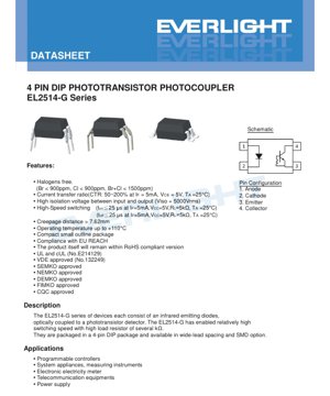
4.2 Pin Configuration and Polarity
The device utilizes a standard 4-pin DIP pin arrangement:
- Pin 1: Anode (Input LED)
- Pin 2: Cathode (Input LED)
- Pin 3: Emitter (Output Phototransistor)
- Pini 4: Kolekta (Pato la fototransista)
4.3 Recommended PCB Pad Layout
For surface-mount options (S1 and S2), the datasheet provides recommended pad layouts. These are reference designs intended to ensure reliable soldering and mechanical stability. The document explicitly states that these dimensions should be modified based on specific manufacturing processes and requirements (such as solder paste volume and thermal relief considerations).
5. Soldering and Assembly Guide
The soldering temperature (TSOL) rating for this device is 260°C for a maximum of 10 seconds. This is consistent with typical lead-free reflow profiles. For through-hole packages using wave soldering, standard industry practices should be followed, taking care not to exceed the maximum body temperature of the package. The storage temperature range is -55°C to +125°C. For SMD assembly, it is recommended to store the device in moisture barrier packaging, and if the moisture exposure level is exceeded, appropriate baking procedures should be followed.
6. Packaging and Ordering Information
Msimbo wa kuagiza unafuata muundo ufuatao: EL2514X(Y)-VG.
- X:Chaguo za umbo la pini (S1, S2, M, au kuacha wazi kwa DIP ya kawaida).
- Y:Tape and reel packaging options (TU, TD, or leave blank for tube).
- V:Inaonyesha uthibitisho wa usalama wa VDE (hiari).
- G:Inaonyesha muundo usio na halojeni.
7. Mapendekezo ya Utumiaji
7.1 Matumizi ya Kawaida
EL2514-G inafaa kabisa kwa matumizi yanayohitaji kutengwa kwa umeme, upinzani wa kelele, au ubadilishaji wa viwango. Matumizi maalum yaliyotajwa ni pamoja na:
- Programmable Logic Controller (PLC):Used to isolate digital I/O modules from the central processing unit and field devices.
- System Equipment and Measuring Instruments:Kutenganishwa kwa ishara za sensor au mistari ya mawasiliano katika vifaa vya viwanda.
- Mita ya umeme ya elektroniki:Kutoa kutenganishwa katika saketi ya kipimo ili kuhakikisha usalama na kuzuia kelele.
- Vifaa vya mawasiliano:Signal isolation in data lines or power supply feedback loops.
- Power Supply:Commonly used in the feedback loop of Switch-Mode Power Supplies (SMPS) to isolate the feedback signal from the secondary side from the controller on the primary side, thereby enhancing safety and stability.
7.2 Mambo ya Kuzingatia katika Ubunifu
- CTR Variation:When designing the receiving circuit (e.g., comparator threshold, pull-up resistor value), ensure it operates reliably across the entire CTR range of 50-200%.
- Kasi na Mzigo:Kasi ya kubadili imebainishwa chini ya mzigo wa 5 kΩ. Kutumia upinzani wa mzigo mdogo kwa kawaida huongeza kasi ya kubadili, lakini hupunguza mwingilio wa pato na kuongeza matumizi ya nguvu. Upinzani mkubwa zaidi hupunguza kasi ya kuitikia, hasa wakati wa kuzima, kutokana na muda wa kuhifadhi wa transistor ya mwanga.
- Kikomo cha Mkondo wa LED:Hakikisha unatumia upinzani wa mfululizo ili kuzuia mkondo wa mbele (IF) ndani ya anuwai ya kazi inayopendekezwa (kawaida 5-7 mA) au chini ya thamani kamili ya juu. Hii inahakikisha uimara wa muda mrefu na uwiano thabiti wa uhamishaji wa mkondo (CTR).
- Ukinzani wa kelele:Ingawa kuunganisha kwa mwanga (photocoupler) hutoa ukandamizaji bora wa hali ya kawaida, muundo sahihi wa bodi ya mzunguko uliochapishwa (PCB) unapaswa kuhakikishwa kwa kuzuia kelele za masafa ya juu kwa kuhifadhi nyuzi za pembejeo na pato zikitengwa na kutumia kondakta za kupita karibu na pini za kifaa.
8. Technical Comparison and Positioning
EL2514-G hutofautishwa katika soko kwa kuchanganya sifa muhimu. Voltage yake ya juu ya kutengwa (5000 Vrms) na umbali mrefu wa kupanda umeme hufanya iwe mteule mzuri kwa matumizi yenye mahitaji madhubuti ya usalama. Muundo usio na halojeni unakidhi kanuni za kimazingira na upendeleo wa wateja kwa vifaa vya elektroniki "vya kijani". Uhakikisho mpana (UL, VDE, n.k.) hupunguza vikwazo vya uthibitishaji kwa bidhaa za mwisho zinazolenga soko la kimataifa. Ingawa kasi yake ya kubadili (25 µs) inafaa kwa matumizi mengi ya kutengwa kidijitali na mrejesho wa umeme, haijaainishwa kama kiunganishi cha haraka sana cha mawasiliano ya data; matumizi hayo yanahitaji vifaa vilivyo na wakati wa kubadili wa kiwango cha nanosekunde. Kwa hivyo, EL2514-G inapaswa kuonwa kama kiunganishi cha nuru kinachostahimili, cha matumizi mengi, kilichoboreshwa kwa kuaminika, kufuata usalama, na utendaji wa wastani.
9. Frequently Asked Questions (Based on Technical Parameters)
Swali: Inamaanisha nini kwa muundo wangu wa saketi anuwai ya CTR ya 50-200%?
Jibu: Hii inamaanisha ya kwamba mkondo wa pato unaweza kuwa chini hadi nusu ya mkondo wa kuingiza, au juu hadi mara mbili yake. Saketi yako lazima ifanye kazi vizuri katika hali zote mbili za mwisho. Kwa kiolesura cha dijiti, hii inaathiri uchaguzi wa upinzani wa kuinua (pull-up) na kizingiti cha kuingiza cha geti inayofuata au kidhibiti-kichakato (microcontroller).
Swali: Je, naweza kutumia chanzo cha voltage kuendesha LED moja kwa moja?
A: Hapana. LED ni kifaa kinachoendeshwa na mkondo. Lazima uwe unatumia daima kizuizi cha mkondo kwenye mfululizo na LED ili kuweka I inayohitajika.Fna kuzuia uharibifu wa mkondo kupita kiasi, hata kama voltage ya usambazaji wako inalingana na V ya kawaida.F.
Q: Voltage ya kutengwa ni 5000 Vrms. Je, hii inamaanisha naweza kutumia voltage ya 5000V kwa uendelevu kati ya pembejeo na pato?
A: Hapana. Hii ni thamani ya uvumilivu wa voltage iliyojaribiwa kwa dakika moja chini ya hali zilizodhibitiwa. Voltage ya kazi ya kuendelea katika matumizi inapaswa kuwa chini sana kuliko hii, inafafanuliwa na viwango vya usalama vinavyohusiana vya kifaa cha mwisho.
Swali: Kuna tofauti gani kati ya chaguo S1 na S2?
Jibu: Tofauti kuu iko katika ukubwa wa ufungashaji na ukubwa wa mkanda wa kuviringisha. Upana wa kiini cha S2 (kipimo B0) ni mkubwa kidogo, na hutumia mkanda mpana zaidi (S1 ni 16mm, S2 ni 24mm), na kila mkanda unaweza kubeba vifaa zaidi (S1 ni 1500, S2 ni 2000). Uchaguzi unategemea vikwazo vya nafasi kwenye PCB yako na utangamano wa feeder ya mstari wa usanikishaji.
10. Mifano Halisi ya Ubunifu
Scenario: Isolating the digital signal of a microcontroller to the high-voltage section.
A microcontroller (3.3V logic) needs to send an ON/OFF signal to a circuit operating at a different and noisy high-voltage potential. The EL2514-G can be used for isolation.
Design Steps:
- Upande wa Ingizo:Kupitia kizuizi cha upinzani wa umeme (Rlimit) Unganisha pini ya GPIO ya microcontroller kwenye anode ya optocoupler. Hesabu Rlimit= (VCC_MCU- VF) / IF. For VCC_MCU=3.3V, VF~1.2V, target IF=5mA, then Rlimit= (3.3-1.2)/0.005 = 420Ω. Tumia upinzani wa kawaida wa 470Ω. Unganisha cathode kwenye ardhi.
- Upande wa pato:Unganisha collector kwenye upinzani wa kuvuta (RL). Unganisha emitter kwenye ardhi iliyotengwa. RLThamani yake huathiri kasi na mkondo. Kutumia upinzani wa 5kΩ katika hali ya majaribio ya karatasi ya data hutoa muda maalum wa kubadili. Kisha, ishara kutoka kwenye nodi ya kolekta inaweza kuendesha mlango wa MOSFET upande wa kutengwa au ingizo lingine la mantiki.
- Mpangilio:Tenga kimwili sehemu za ingizo na pato kwenye PCB. Weka umbali wa kutambaa zaidi ya milimita 7.62 kulingana na uwezo wa kifuniko. Weka kondakta dogo la kupita (mfano 0.1µF) karibu na pini za kifaa kati ya nguvu na ardhi pande zote mbili za kuunganisha.
11. Kanuni za Uendeshaji
Kipishaji cha mwanga na umeme ni kifaa kinachotumia mwanga kuhamisha ishara za umeme kati ya saketi mbili zilizotengwa. Katika EL2514-G, mkondo unaotumika kwenye pini za pembejeo (1 na 2) husababisha diode inayotoa mwanga wa infrared (LED) kutolea fotoni. Fotoni hizi hupita kwenye pengo la wazi la kuzuia (kwa kawaida linalotengenezwa kwa misombo iliyochujwa) na kugonga eneo la msingi la transistor ya fotoni ya silikoni upande wa pato (pini 3 na 4). Mwanga unaoingia husababisha jozi za elektroni na shimo katika eneo la msingi, kazi kwa ufanisi kama mkondo wa msingi. Kisha, mkondo huu wa msingi unaozalishwa na mwanga unakuza kwa faida ya transistor, na kuzalisha mkondo wa kolekta (IC) sawia na mkondo wa pembejeo wa LED (IF). Uwiano IC/IFNi uwiano wa uhamishaji wa mkondo (CTR). Jambo muhimu ni kwamba muunganisho pekee kati ya pembejeo na pato ni mwanga, na hivyo kutoa kutengwa kwa umeme.
12. Mwelekeo wa Teknolojia
Soko la viunganishi vya mwanga na umeme linaendelea kukua. Mienendo inayoathiri vifaa kama vile EL2514-G ni pamoja na:
- Kuongeza kiwango cha ushirikiano:Kuchanganya njia nyingi za kutengwa pamoja, au kuunganisha utendaji wa ziada kama vile kiendeshi cha lango au kikukuza kosa ndani ya kifurushi kimoja.
- Kukuza viunganishi vinavyotumia vigunduzi vya haraka (kama vile photodiode yenye kikukuza kilichounganishwa) ili kusaidia itifaki za mawasiliano ya dijiti za kiwango cha Mbps (USB, CAN, RS-485).Kuongeza Uaminifu na Maisha ya Huduma:
- Kulenga kuboresha uthabiti wa muda mrefu wa CTR, ambayo hupungua kwa muda kutokana na uzee wa LED (hasa kwenye joto la juu na mkondo mkubwa).Uzingatiaji Mkali zaidi wa Mazingira:
- Zaidi ya RoHS na halojeni-bure, umakini unaongezeka kwenye mnyororo wa usambazaji kuhusu vitu kama PFAS na viashiria vya upendeleo zaidi endelevu.Mbinu mbadala za kutenganisha:
- Ingawa optocouplers bado zinatawala katika matumizi mengi, utenganishaji wa capacitive (kutumia SiOkizuizi) na utenganishaji wa sumaku (kutumia transfoma) zinashindana katika nyanja zinazohitaji kasi kubwa sana, matumizi ya nguvu ya chini, au msongamano wa juu wa ujumuishaji. Optocouplers zinaendelea kuwa na faida katika urahisi, upinzani wa juu wa mishtuko ya hali ya kawaida (CMTI), na uthibitisho wa usalama uliokomaa.2EL2514-G inalenga uthibitisho wa usalama, kufuata mazingira, na utendaji thabiti, ikikidhi mahitaji ya kudumu katika soko la viwanda, umeme na vifaa ambapo mwelekeo huu ni muhimu.
Maelezo ya kina ya istilahi za vipimo vya LED
Ufafanuzi kamili wa istilahi za kiteknolojia ya LED
I. Viashiria Muhimu vya Utendaji wa Kielektroniki na Mwanga
| Istilahi | Unit/Representation | Layman's Explanation | Why It Is Important |
|---|---|---|---|
| Ufanisi wa Mwanga (Luminous Efficacy) | lm/W (lumen kwa watt) | Kiasi cha mwanga kinachotolewa kwa kila wati wa umeme, cha juu zaidi ndivyo kinavyotumia nishati kwa ufanisi zaidi. | Huamua moja kwa moja kiwango cha ufanisi wa nishati ya taa na gharama ya umeme. |
| Luminous Flux | lm (lumen) | Jumla ya kiasi cha mwanga kinachotolewa na chanzo cha mwanga, kinachojulikana kwa kawaida kama "mwangaza". | Kuamua kama taa inatoa mwanga wa kutosha. |
| Pembe ya kuona mwanga (Viewing Angle) | ° (digrii), kama 120° | Pembe wakati ukali wa mwanga unapungua kwa nusu, huamua upana wa boriti ya mwanga. | Huathiri eneo la mwangaza na usawa wake. |
| Joto la rangi (CCT) | K (Kelvin), k.m. 2700K/6500K | Joto la rangi ya mwanga, thamani ya chini huelekea manjano/joto, thamani ya juu huelekea nyeupe/baridi. | Huamua mazingira ya taa na matumizi yanayofaa. |
| Kielelezo cha Uonyeshaji Rangi (CRI / Ra) | No unit, 0–100 | The ability of a light source to reproduce the true colors of objects, Ra≥80 is recommended. | Affects color fidelity, used in high-demand places such as shopping malls and art galleries. |
| Tofauti ya rangi (SDCM) | Hatua za duaradufu ya MacAdam, k.m. "5-step" | Kipimo cha nambari cha usawa wa rangi, hatua ndogo zaidi inaonyesha usawa mkubwa wa rangi. | Hakikisha hakuna tofauti ya rangi kati ya taa za kundi moja. |
| Dominant Wavelength | nm (nanomita), k.m. 620nm (nyekundu) | Thamani ya wavelength inayolingana na rangi ya LED ya rangi. | Amua rangi ya LED za rangi moja kama nyekundu, manjano, kijani, n.k. |
| Spectral Distribution | Wavelength vs. Intensity Curve | Inaonyesha usambazaji wa ukubwa wa mwanga katika kila urefu wa wimbi unaotolewa na LED. | Inaathiri ubora wa kuonyesha rangi na ubora wa rangi. |
II. Vigezo vya Umeme
| Istilahi | Ishara | Layman's Explanation | Uzingatiaji wa Ubunifu |
|---|---|---|---|
| Voltage ya Mbele (Forward Voltage) | Vf | Voltage ya chini inayohitajika kuwasha LED, kama "kizingiti cha kuanzisha". | Voltage ya chanzo cha usukumaji lazima iwe ≥ Vf, voltage inajumlishwa wakati LED nyingi zimeunganishwa mfululizo. |
| Forward Current | If | The current value that allows the LED to emit light normally. | Mara nyingi hutumia usukumaji wa mkondo wa mara kwa mara, mkondo huamua mwangaza na maisha ya taa. |
| Mkondo wa juu zaidi wa msukumo (Pulse Current) | Ifp | Kilele cha mkondo kinachoweza kustahimili kwa muda mfupi, kinachotumiwa kwa kudimisha au kumulika. | Upana wa msukumo na uwiano wa wakati wa kufanya kazi lazima udhibitiwe kwa uangalifu, vinginevyo kuharibika kwa joto kupita kiasi. |
| Reverse Voltage | Vr | The maximum reverse voltage that an LED can withstand; exceeding it may cause breakdown. | Mzunguko unahitaji kuzuia kuingizwa kinyume au mshtuko wa voltage. |
| Thermal Resistance | Rth (°C/W) | Upinzani wa joto kutoka kwenye chip hadi kwenye sehemu ya kuunganishia, thamani ya chini inaonyesha usambazaji bora wa joto. | Upinzani mkubwa wa joto unahitaji muundo wenye nguvu zaidi wa kupoza joto, vinginevyo joto la kiungo litaongezeka. |
| Uvumilivu wa kutokwa umeme tuli (ESD Immunity) | V (HBM), k.m. 1000V | Uwezo wa kupiga umeme wa tuli, thamani ya juu haifanyi uharibifu wa umeme wa tuli. | Hatua za kuzuia umeme wa tuli zinahitajika katika uzalishaji, hasa kwa LED zenye usikivu mkubwa. |
Tatu, Usimamizi wa Joto na Uaminifu
| Istilahi | Viashiria Muhimu | Layman's Explanation | Athari |
|---|---|---|---|
| Joto la Kiungo (Junction Temperature) | Tj (°C) | Joto halisi la uendeshaji ndani ya Chip ya LED. | For every 10°C reduction, the lifespan may double; excessively high temperatures lead to lumen depreciation and color shift. |
| Lumen Depreciation | L70 / L80 (saa) | Muda unaohitajika ili mwangaza upunguke hadi 70% au 80% ya thamani ya awali. | Kufafanua moja kwa moja "maisha ya huduma" ya LED. |
| Lumen Maintenance | % (e.g., 70%) | Asilimia ya mwangaza uliobaki baada ya kutumia kwa muda fulani. | Inaonyesha uwezo wa kudumisha mwangaza baada ya matumizi ya muda mrefu. |
| Color Shift | Δu′v′ or MacAdam Ellipse | The degree of color change during usage. | Inaathiri usawa wa rangi katika mandhari ya taa. |
| Uzeefu wa joto (Thermal Aging) | Kupungua kwa utendaji wa nyenzo | Uharibifu wa nyenzo za ufungaji unaosababishwa na joto la muda mrefu. | Inaweza kusababisha kupungua kwa mwangaza, mabadiliko ya rangi, au kushindwa kwa mzunguko wazi. |
IV. Ufungaji na Nyenzo
| Istilahi | Aina za Kawaida | Layman's Explanation | Sifa na Matumizi |
|---|---|---|---|
| Aina ya Ufungashaji | EMC, PPA, Kauri | Nyenzo za kifuniko zinazolinda chip na kutoa mwingiliano wa mwanga na joto. | EMC ina msimamo mzuri dhidi ya joto na gharama nafuu; kauri ina ufanisi bora wa upunguzaji joto na maisha marefu. |
| Muundo wa chip | Front-side, Flip Chip | Chip Electrode Layout. | Inverted mounting offers better heat dissipation and higher luminous efficacy, making it suitable for high-power applications. |
| Phosphor coating | YAG, silicate, nitride | Coated on the blue LED chip, partially converted to yellow/red light, mixed to form white light. | Different phosphors affect luminous efficacy, color temperature, and color rendering. |
| Lens/Optical Design | Flat, Microlens, Total Internal Reflection | Optical structures on the encapsulation surface control light distribution. | Determines the emission angle and light distribution curve. |
V. Quality Control and Binning
| Istilahi | Bin Content | Layman's Explanation | Purpose |
|---|---|---|---|
| Luminous Flux Binning | Codes such as 2G, 2H | Grouped by brightness level, each group has a minimum/maximum lumen value. | Hakikisha mwangaza wa bidhaa za kundi moja unaolingana. |
| Voltage binning | Codes such as 6W, 6X | Grouped by forward voltage range. | Facilitates driver power supply matching and improves system efficiency. |
| Color Grading | 5-step MacAdam ellipse | Group by color coordinates to ensure colors fall within a minimal range. | Ensure color consistency to avoid uneven colors within the same luminaire. |
| Color temperature binning | 2700K, 3000K, n.k. | Pangwa kundi kulingana na joto la rangi, kila kundi kina anuwai ya kuratibu inayolingana. | Kukidhi mahitaji ya joto la rangi kwa matukio tofauti. |
Sita, Uchunguzi na Uthibitishaji
| Istilahi | Kigezo/Uchunguzi | Layman's Explanation | Maana |
|---|---|---|---|
| LM-80 | Mtihani wa Kudumisha Lumen | Long-term illumination under constant temperature conditions, recording brightness attenuation data. | Used to estimate LED lifetime (in conjunction with TM-21). |
| TM-21 | Life Projection Standard | Projecting lifetime under actual use conditions based on LM-80 data. | Toa utabiri wa kisayansi wa maisha. |
| IESNA standard | Illuminating Engineering Society Standards | Covers optical, electrical, and thermal test methods. | Industry-recognized testing basis. |
| RoHS / REACH | Environmental certification | Hakikisha bidhaa hazina vitu hatari (kama risasi, zebaki). | Masharti ya kuingia soko la kimataifa. |
| ENERGY STAR / DLC | Uthibitisho wa Ufanisi wa Nishati | Uthibitisho wa Ufanisi wa Nishati na Utendaji kwa Bidhaa za Taa. | Inatumika kwa shughuli za ununuzi wa serikali na miradi ya ruzuku, kuimarisha ushindani wa soko. |