Orodha ya Yaliyomo
- 1. Muhtasari wa Bidhaa
- 2. Uchunguzi wa kina wa Vigezo vya Kiufundi
- 2.1 Viwango vya Juu Kabisa
- 2.2 Tabia za Umeme na Mwanga
- 2.2.1 Tabia za Ingizo (Upande wa LED)
- 2.2.2 Tabia za Pato (Upande wa Phototransistor)
- 2.2.3 Tabia za Uhamishaji
- 3. Maelezo ya Mfumo wa Kupanga Daraja
- 4. Uchambuzi wa Mviringo wa Utendaji
- 5. Taarifa za Mitambo na Kifurushi
- 5.1 Usanidi wa Pini
- 5.2 Vipimo vya Kifurushi na Ukubwa wa Nyayo
- 6. Miongozo ya Kuuza na Usanikishaji
- 7. Taarifa za Ufungaji na Kuagiza
- 7.1 Kanuni ya Kuhesabu Nambari ya Mfano
- 7.2 Vipimo vya Ufungaji
- 7.3 Alama ya Kifaa
- 8. Mapendekezo ya Matumizi
- 8.1 Saketi za Kawaida za Matumizi
- 8.2 Mambo ya Kuzingatia katika Ubunifu
- 9. Ulinganisho wa Kiufundi na Faida
- 10. Maswali Yanayoulizwa Mara kwa Mara (Kulingana na Vigezo vya Kiufundi)
- 11. Uchunguzi wa Kesi ya Ubunifu wa Vitendo
- 12. Kanuni ya Uendeshaji
- 13. Mienendo ya Sekta
1. Muhtasari wa Bidhaa
Mfululizo wa EL101XH-G unawakilisha familia ya photocouplers za phototransistor zenye utendaji wa juu (optocouplers) zilizoundwa kwa ajili ya utofautishaji thabiti wa ishara katika matumizi magumu ya elektroniki. Vifaa hivi vimeundwa kutoa kizuizi thabiti cha galvaniki kati ya saketi za ingizo na pato, kuzuia vitanzi vya ardhi, mipigo ya voltage, na kelele kusambaa kati ya sehemu tofauti za mfumo. Kazi kuu hufikiwa kwa diode inayotoa mwanga wa infrared inayounganishwa kwa mwanga kwa kigunduzi cha phototransistor cha silikoni, yote yakiwa ndani ya kifurushi kidogo cha 4-pin Small Outline Package (SOP).
Kipengele kikuu cha kutofautisha cha mfululizo huu niumbali mrefu wa creepage wa 8mm, ambao huongeza kwa kiasi kikubwa usalama na uaminifu katika matumizi yanayohitaji voltage za juu za utofautishaji. Ubunifu huu, ukichanganywa na5000 Vrmskiwango cha voltage ya utofautishaji, hufanya mfululizo huu ufawe kwa mifumo ya udhibiti wa viwanda, vifaa vya usambazaji wa umeme, na vifaa ambapo usalama wa mtumiaji na ulinzi wa vifaa ni muhimu zaidi. Vifaa hivi pia hutengenezwa kuwabila halojeni, kuzingatia kanuni za kimazingira kwa kuzuia maudhui ya bromini (Br) na klorini (Cl).
Soko la lengo la mfululizo wa EL101XH-G ni pana, likijumuisha otomatiki ya viwanda, mawasiliano, vyombo vya kupimia, na vifaa vya watumiaji. Matumizi ya kawaida ni pamoja na utofautishaji katika moduli za I/O za programu ya udhibiti wa mantiki (PLC), usambazaji wa ishara katika vifaa vya mawasiliano, utofautishaji wa kiolesura katika vyombo vya kupimia, na utofautishaji wa usalama katika vifaa vya nyumbani kama vile jiko la joto la upepo.
. Technical Parameter Deep-Dive
.1 Absolute Maximum Ratings
These ratings define the stress limits beyond which permanent damage to the device may occur. Operation under or at these limits is not guaranteed.
- Input Forward Current (IF): 50 mA (Continuous). This is the maximum DC current that can be passed through the input infrared LED.
- Peak Forward Current (IFP): 1 A for 1 µs pulse. This rating is crucial for withstanding brief current surges during switching events.
- Input Reverse Voltage (VR): 6 V. Exceeding this voltage in reverse bias can damage the LED.
- Output Collector-Emitter Voltage (VCEO): 80 V. This is the maximum voltage the phototransistor's collector can withstand relative to its emitter when the base (driven by light) is open.
- Total Power Dissipation (PTOT): 250 mW. This is the maximum combined power the entire device can dissipate, limiting the product of input current/voltage and output current/voltage.
- Isolation Voltage (VISO): 5000 Vrmsfor 1 minute. This critical safety parameter is tested with pins 1 & 2 shorted together and pins 3 & 4 shorted together, applying high voltage between these two groups.
- Operating Temperature (TOPR): -55°C to +125°C. This wide range ensures functionality in harsh industrial and automotive environments.
- Soldering Temperature (TSOL): 260°C for 10 seconds. This guides the reflow soldering process.
.2 Electro-Optical Characteristics
These parameters define the device's performance under normal operating conditions (Ta= 25°C unless noted).
.2.1 Input Characteristics (LED Side)
- Forward Voltage (VF): Typically 1.2V, with a maximum of 1.4V at IF= 10 mA. This is used to calculate the required current-limiting resistor.
- Reverse Current (IR): Maximum 10 µA at VR= 6V, indicating good diode leakage characteristics.
- Input Capacitance (Cin): Typically 50 pF. This affects high-frequency switching performance on the input side.
.2.2 Output Characteristics (Phototransistor Side)
- Collector-Emitter Dark Current (ICEO): Maximum 200 nA at VCE= 48V, IF= 0mA. This is the leakage current when the LED is off, important for off-state signal integrity.
- Collector-Emitter Breakdown Voltage (BVCEO): Minimum 80V at IC= 0.1mA, confirming the high voltage capability.
- Collector-Emitter Saturation Voltage (VCE(sat)): Maximum 0.3V at IF= 10mA, IC= 1mA. A low saturation voltage is desirable when the output is used as a switch in the "on" state.
.2.3 Transfer Characteristics
These parameters define the coupling efficiency and speed between input and output.
- Current Transfer Ratio (CTR): This is the core performance metric, defined as (IC/ IF) * 100% at specified conditions (VCE=5V, IF=5mA). The EL101XH-G series is offered in multiple CTR grades:
- EL1010H: 50% to 600% (Wide range)
- EL1011H: 100% to 200%
- EL1017H: 80% to 160%
- EL1018H: 130% to 260%
- EL1019H: 200% to 400%
- Isolation Resistance (RIO): Minimum 5 x 10¹⁰Ω at 500V DC. This extremely high resistance confirms the quality of the internal insulation material.
- Floating Capacitance (CIO): Maximum 1.0 pF. This low inter-package capacitance is key for achieving high common-mode transient immunity (CMTI) in noisy environments.
- Switching Times: Tested with VCE=5V, IC=5mA, RL=100Ω.
- Turn-on time (ton): Typically 12 µs.
- Turn-off time (toff): Typically 10 µs.
- Rise time (tr) and Fall time (tf): Maximum 18 µs each.
. Grading System Explanation
The EL101XH-G series utilizes aCTR-based grading system, which is the primary differentiator between part numbers. The "X" in the part number EL101XH-G denotes the CTR rank (0, 1, 7, 8, 9). Each rank corresponds to a specific minimum and typical CTR range, as detailed in section 2.2.3. This allows designers to select a device with the precise gain needed for their application. Choosing a higher CTR grade (e.g., EL1019H) can reduce the required drive current for the input LED, lowering power consumption and heat generation. Conversely, a lower CTR grade might be sufficient for applications with ample drive current available.
. Performance Curve Analysis
While the PDF indicates the presence of "Typical Electro-Optical Characteristics Curves," the specific graphs are not provided in the text content. Typically, such datasheets include curves showing the relationship between:
- CTR vs. Forward Current (IF): This curve shows how the current transfer ratio changes with the LED drive current. CTR often decreases at very high IFdue to heating and efficiency droop.
- CTR vs. Ambient Temperature (Ta): This is a critical curve for thermal design. CTR for phototransistor couplers typically has a negative temperature coefficient, meaning it decreases as temperature increases. Designers must account for this derating over the full operating temperature range.
- Collector Current vs. Collector-Emitter Voltage (IC-VCE): These output characteristic curves, plotted for different input currents (IF), show the phototransistor's operating regions (saturation, active).
- Forward Voltage vs. Forward Current (VF-IF): The standard LED I-V curve, useful for thermal management of the input side.
Designers should consult the official datasheet with graphical plots to accurately model device behavior under non-standard conditions.
. Mechanical and Package Information
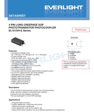
.1 Pin Configuration
The 4-pin SOP package has the following pinout:
- Anodeof the input infrared LED.
- Cathodeof the input infrared LED.
- Emitterof the output phototransistor.
- Collectorof the output phototransistor.
.2 Package Dimensions and Footprint
The device is described as a "Compact 4 Pin SOP with a 2.2 mm profile." The PDF includes a "Package Dimension" diagram and a "Recommended pad layout for surface mount." The pad layout suggestion is provided as a reference, and the datasheet explicitly advises designers to modify the pad dimensions based on their specific PCB manufacturing processes and thermal requirements. Proper pad design is essential for reliable soldering and mechanical strength.
. Soldering and Assembly Guidelines
The key parameter provided is thesoldering temperature: 260°C for 10 seconds. This aligns with typical lead-free reflow soldering profiles (IPC/JEDEC J-STD-020). Designers and manufacturers must ensure their reflow oven profile does not exceed this time-at-temperature to prevent damage to the internal epoxy mold compound and the wire bonds. Standard handling procedures for moisture-sensitive devices (MSL rating, which is not specified in the provided text but should be checked in the full datasheet) should be followed, including baking if the packaging has been exposed to ambient humidity beyond its rated level.
. Packaging and Ordering Information
.1 Model Numbering Rule
The part number follows the format:EL101X H(Y)- VG
- EL101: Base part number.
- X: CTR Rank (0, 1, 7, 8, 9).
- H: Denotes high-temperature operation capability.
- (Y): Tape and reel option. Can be TA, TB, or none (for tube packaging).
- V: Optional suffix denoting VDE safety certification.
- G: Denotes halogen-free construction.
.2 Packaging Specifications
The device is available in two main packaging forms:
- Tube: 100 units per tube. Options are standard or with VDE certification.
- Tape and Reel: 3000 units per reel. Two feed direction options are available (TA and TB), with detailed tape dimensions (Ao, Bo, Po, P, etc.) provided in the datasheet for automated pick-and-place machine programming.
.3 Device Marking
The top of the SOP package is marked with a code:EL 101X H Y WW V
- EL: Manufacturer code.
- X: Device number (X indicates CTR rank).
- H: High-temperature operating designation.
- Y: 1-digit year code.
- WW: 2-digit week code.
- V: Optional marking for VDE-approved versions.
. Application Recommendations
.1 Typical Application Circuits
The photocoupler can be used in two primary modes:
- Digital Switching / Isolation: The input LED is driven by a digital signal (e.g., from a microcontroller GPIO). The phototransistor output acts as a switch, pulling a line to ground or VCCthrough a pull-up resistor. The switching time specifications determine the maximum data rate.
- Linear Signal Isolation: By operating the phototransistor in its active region (not saturated), it can be used to transmit analog signals. However, the non-linear CTR and its variation with temperature make this challenging without additional compensation circuitry. It is more common to use a dedicated linear optocoupler for such tasks.
.2 Design Considerations
- Input Current Limiting: An external resistor isalwaysrequired in series with the input LED to set the forward current (IF). Calculate Rlimit= (Vdrive- VF) / IF. Ensure IFdoes not exceed 50 mA DC.
- CTR Derating with Temperature: Account for the decrease in CTR at high temperatures. Design the circuit to function correctly at the maximum operating temperature with the minimum CTR from the selected grade.
- Output Load Resistor (RL): The value of the pull-up resistor on the collector affects switching speed, power consumption, and noise immunity. A smaller RLgives faster switching but higher current draw. The test condition of RL= 100Ω is for characterization; practical values often range from 1kΩ to 10kΩ.
- Noise Immunity: The low coupling capacitance (<1pF) provides good common-mode rejection. For very noisy environments, ensure a clean layout with proper grounding and consider adding a small bypass capacitor (e.g., 0.1µF) across the output side supply rails.
. Technical Comparison and Advantages
The EL101XH-G series differentiates itself in the market through several key features:
- Long Creepage Distance (8mm): Compared to standard SOP optocouplers, this extended creepage is a significant advantage for applications requiring reinforced insulation or operating in polluted environments, as it reduces the risk of surface tracking.
- High Isolation Voltage (5000Vrms): This is a robust isolation rating suitable for industrial mains-connected equipment (e.g., 240V/480V systems).
- Halogen-Free Compliance: Meets environmental and regulatory requirements for reduced halogen content, which is increasingly important in green electronics.
- Wide Operating Temperature Range (-55°C to +125°C): Exceeds the typical commercial range (0°C to 70°C), making it fit for industrial, automotive, and military-grade applications.
- Pending Safety Approvals: The datasheet lists approvals from UL, cUL, VDE, SEMKO, NEMKO, DEMKO, FIMKO, and CQC as "pending." This indicates the device is designed to meet these stringent international safety standards.
. Frequently Asked Questions (Based on Technical Parameters)
Q1: What is the purpose of the long creepage distance?
A1: Creepage distance is the shortest path along the surface of the insulating package between two conductive parts (input and output pins). An 8mm distance increases protection against high-voltage arcing or tracking across the package surface, especially in humid or contaminated environments, enhancing long-term reliability and safety.
Q2: How do I choose the right CTR grade?
A2: Select based on your available drive current and required output current. If your microcontroller can only provide 5mA, choose a high-CTR grade (e.g., EL1019H) to get sufficient output current. If you have ample drive current, a lower grade may be more cost-effective. Always design for the worst-case (minimum CTR at maximum temperature).
Q3: Can this be used for AC signal isolation?
A3: The phototransistor output is unidirectional (current flows from Collector to Emitter). To isolate an AC signal, you would typically use two devices in inverse-parallel configuration or a dedicated AC-input optocoupler. For digital AC zero-crossing detection, it can be used with a bridge rectifier on the input.
Q4: What is the difference between isolation voltage and collector-emitter voltage rating?
A4: Isolation voltage (5000Vrms) is the dielectric withstand voltagebetweenthe input and output sides of the package. Collector-emitter voltage (80V) is the maximum voltage that can be appliedacross the output transistor itselfduring normal operation. They are completely different parameters.
. Practical Design Case Study
Scenario:Isolating a 3.3V microcontroller GPIO signal to control a 24V relay coil on a separate power domain in an industrial PLC module.
Design Steps:
- Input Side:The MCU GPIO is 3.3V. Assuming a desired IFof 5mA and a typical VFof 1.2V, calculate Rlimit= (3.3V - 1.2V) / 0.005A = 420Ω. Use a standard 430Ω resistor.
- CTR Selection:The relay coil driver transistor base requires ~5mA. With IF=5mA, minimum required CTR = (5mA / 5mA)*100% = 100%. To ensure operation at 125°C (where CTR is lower), select a grade with comfortable margin. EL1018H (min CTR 130%) is a good choice.
- Output Side:Connect the phototransistor collector to the 24V supply via a pull-up resistor (RL). The emitter connects to the base of the relay driver transistor (an NPN BJT or an N-channel MOSFET gate). When the MCU output is high, the LED is on, the phototransistor saturates, pulling the base to near ground, turning off the driver. When the MCU output is low, the LED is off, the phototransistor is off, and a separate bias resistor pulls the driver base high to activate the relay. A snubber diode is required across the relay coil.
- Layout:Keep the input and output traces physically separated on the PCB. Place the bypass capacitors close to the device pins. Follow the recommended pad layout for reliable soldering.
. Operating Principle
A photocoupler (or optocoupler) is a device that transfers electrical signals between two isolated circuits using light. In the EL101XH-G series:
- An electrical current applied to theinput pins (Anode and Cathode)causes the integratedinfrared light-emitting diode (LED)to emit photons.
- These photons travel through a transparent insulating material (typically a molded epoxy) within the package.
- The photons strike the base region of asilicon phototransistoron theoutput side.
- This light energy generates electron-hole pairs in the base, effectively acting as a base current and causing the transistor to conduct between itsCollector and Emitter pins.
- The amount of output collector current (IC) is proportional to the input LED current (IF), with the proportionality constant being the Current Transfer Ratio (CTR).
. Industry Trends
The market for isolation components like photocouplers is evolving driven by several key trends:
- Higher Speed and Bandwidth:Demand is growing for digital isolators and high-speed optocouplers capable of supporting communication protocols like USB, CAN FD, and Ethernet in isolated networks, pushing data rates into the tens and hundreds of Mbps.
- Integration:There is a trend towards integrating multiple isolation channels into a single package, or combining isolation with other functions like gate drivers for power MOSFETs/IGBTs.
- Enhanced Safety and Reliability Standards:Regulations in industrial, automotive (ISO 26262), and medical equipment continue to tighten, requiring components with higher certified isolation ratings, longer creepage/clearance, and proven reliability data.
- Miniaturization:While maintaining or improving isolation performance, packages are becoming smaller (e.g., wide-body SOIC, DSOP) to save board space.
- Alternative Technologies:Photocouplers face competition from capacitive and magnetic (transformer-based) isolation technologies, which can offer advantages in speed, power consumption, and integration. However, optocouplers retain strong advantages in simplicity, high common-mode transient immunity (CMTI), and well-established safety certifications.
Istilahi ya Mafanikio ya LED
Maelezo kamili ya istilahi za kiufundi za LED
Utendaji wa Fotoelektriki
| Neno | Kipimo/Uwakilishaji | Maelezo Rahisi | Kwa Nini Muhimu |
|---|---|---|---|
| Ufanisi wa Mwanga | lm/W (lumen kwa watt) | Pato la mwanga kwa watt ya umeme, juu zaidi inamaanisha ufanisi zaidi wa nishati. | Moja kwa moja huamua daraja la ufanisi wa nishati na gharama ya umeme. |
| Mtiririko wa Mwanga | lm (lumen) | Jumla ya mwanga unaotolewa na chanzo, kwa kawaida huitwa "mwangaza". | Huamua ikiwa mwanga ni mkali wa kutosha. |
| Pembe ya Kutazama | ° (digrii), k.m., 120° | Pembe ambayo ukali wa mwanga hupungua hadi nusu, huamua upana wa boriti. | Husaidiana na anuwai ya taa na usawa. |
| Joto la Rangi | K (Kelvin), k.m., 2700K/6500K | Uzito/baridi ya mwanga, thamani za chini ni za manjano/moto, za juu ni nyeupe/baridi. | Huamua mazingira ya taa na matukio yanayofaa. |
| Kiwango cha Kurejesha Rangi | Hakuna kipimo, 0–100 | Uwezo wa kuonyesha rangi za vitu kwa usahihi, Ra≥80 ni nzuri. | Husaidiana na ukweli wa rangi, hutumiwa katika maeneo yenye mahitaji makubwa kama vile maduka makubwa, makumbusho. |
| UVumilivu wa Rangi | Hatua za duaradufu za MacAdam, k.m., "hatua 5" | Kipimo cha uthabiti wa rangi, hatua ndogo zina maana rangi thabiti zaidi. | Inahakikisha rangi sawa katika kundi moja ya LED. |
| Urefu wa Mawimbi Kuu | nm (nanomita), k.m., 620nm (nyekundu) | Urefu wa mawimbi unaolingana na rangi ya LED zenye rangi. | Huamua rangi ya LED nyekundu, ya manjano, ya kijani kibichi zenye rangi moja. |
| Usambazaji wa Wigo | Mkondo wa urefu wa mawimbi dhidi ya ukali | Inaonyesha usambazaji wa ukali katika urefu wa mawimbi. | Husaidiana na uwasilishaji wa rangi na ubora. |
Vigezo vya Umeme
| Neno | Ishara | Maelezo Rahisi | Vizingatiaji vya Uundaji |
|---|---|---|---|
| Voltage ya Mbele | Vf | Voltage ya chini kabisa kuwasha LED, kama "kizingiti cha kuanza". | Voltage ya kiendeshi lazima iwe ≥Vf, voltage huongezeka kwa LED zinazofuatana. |
| Mkondo wa Mbele | If | Thamani ya mkondo wa uendeshaji wa kawaida wa LED. | Kwa kawaida kuendesha kwa mkondo wa mara kwa mara, mkondo huamua mwangaza na muda wa maisha. |
| Mkondo wa Pigo wa Juu | Ifp | Mkondo wa kilele unaoweza kustahimili kwa muda mfupi, hutumiwa kwa kudhoofisha au kumulika. | Upana wa pigo na mzunguko wa kazi lazima udhibitiwe kwa ukali ili kuzuia uharibifu. |
| Voltage ya Nyuma | Vr | Voltage ya juu ya nyuma ambayo LED inaweza kustahimili, zaidi ya hapo inaweza kusababisha kuvunjika. | Mzunguko lazima uzuie muunganisho wa nyuma au mipigo ya voltage. |
| Upinzani wa Moto | Rth (°C/W) | Upinzani wa uhamishaji wa joto kutoka chip hadi solder, chini ni bora. | Upinzani wa juu wa moto unahitaji upotezaji wa joto wa nguvu zaidi. |
| Kinga ya ESD | V (HBM), k.m., 1000V | Uwezo wa kustahimili utokaji umeme, juu zaidi inamaanisha hatari ndogo. | Hatua za kuzuia umeme zinahitajika katika uzalishaji, hasa kwa LED nyeti. |
Usimamizi wa Joto na Uaminifu
| Neno | Kipimo Muhimu | Maelezo Rahisi | Athari |
|---|---|---|---|
| Joto la Makutano | Tj (°C) | Joto halisi la uendeshaji ndani ya chip ya LED. | Kila kupungua kwa 10°C kunaweza kuongeza muda wa maisha maradufu; juu sana husababisha kupungua kwa mwanga, mabadiliko ya rangi. |
| Upungufu wa Lumen | L70 / L80 (saa) | Muda wa mwangaza kushuka hadi 70% au 80% ya mwanzo. | Moja kwa moja hufafanua "muda wa huduma" wa LED. |
| Matengenezo ya Lumen | % (k.m., 70%) | Asilimia ya mwangaza uliobakizwa baada ya muda. | Inaonyesha udumishaji wa mwangaza juu ya matumizi ya muda mrefu. |
| Mabadiliko ya Rangi | Δu′v′ au duaradufu ya MacAdam | Kiwango cha mabadiliko ya rangi wakati wa matumizi. | Husaidiana na uthabiti wa rangi katika mandhari ya taa. |
| Kuzeeka kwa Moto | Uharibifu wa nyenzo | Uharibifu kutokana na joto la juu la muda mrefu. | Kunaweza kusababisha kupungua kwa mwangaza, mabadiliko ya rangi, au kushindwa kwa mzunguko wazi. |
Ufungaji na Vifaa
| Neno | Aina za Kawaida | Maelezo Rahisi | Vipengele na Matumizi |
|---|---|---|---|
| Aina ya Kifurushi | EMC, PPA, Kauri | Nyenzo ya nyumba zinazolinda chip, zinazotoa kiolesura cha macho/moto. | EMC: upinzani mzuri wa joto, gharama nafuu; Kauri: upotezaji bora wa joto, maisha marefu. |
| Muundo wa Chip | Mbele, Chip ya Kugeuza | Upangaji wa elektrodi za chip. | Chip ya kugeuza: upotezaji bora wa joto, ufanisi wa juu, kwa nguvu ya juu. |
| Mipako ya Fosforasi | YAG, Siliketi, Nitradi | Inafunika chip ya bluu, inabadilisha baadhi kuwa manjano/nyekundu, huchanganya kuwa nyeupe. | Fosforasi tofauti huathiri ufanisi, CCT, na CRI. |
| Lensi/Optiki | Tambaa, Lensi Ndogo, TIR | Muundo wa macho juu ya uso unaodhibiti usambazaji wa mwanga. | Huamua pembe ya kutazama na mkunjo wa usambazaji wa mwanga. |
Udhibiti wa Ubora na Uainishaji
| Neno | Maudhui ya Kugawa | Maelezo Rahisi | Madhumuni |
|---|---|---|---|
| Bin ya Mtiririko wa Mwanga | Msimbo k.m. 2G, 2H | Imegawanywa kulingana na mwangaza, kila kikundi kina thamani ya chini/ya juu ya lumen. | Inahakikisha mwangaza sawa katika kundi moja. |
| Bin ya Voltage | Msimbo k.m. 6W, 6X | Imegawanywa kulingana na anuwai ya voltage ya mbele. | Hurahisisha mechi ya kiendeshi, huboresha ufanisi wa mfumo. |
| Bin ya Rangi | Duaradufu ya MacAdam ya hatua 5 | Imegawanywa kulingana na kuratibu za rangi, kuhakikisha anuwai nyembamba. | Inahakikisha uthabiti wa rangi, huzuia rangi isiyo sawa ndani ya kifaa. |
| Bin ya CCT | 2700K, 3000K n.k. | Imegawanywa kulingana na CCT, kila moja ina anuwai inayolingana ya kuratibu. | Inakidhi mahitaji tofauti ya CCT ya tukio. |
Kupima na Uthibitishaji
| Neno | Kiwango/Majaribio | Maelezo Rahisi | Umuhimu |
|---|---|---|---|
| LM-80 | Majaribio ya ulinzi wa lumen | Mwanga wa muda mrefu kwa joto la kawaida, kurekodi uharibifu wa mwangaza. | Inatumika kukadiria maisha ya LED (na TM-21). |
| TM-21 | Kiwango cha makadirio ya maisha | Inakadiria maisha chini ya hali halisi kulingana na data ya LM-80. | Inatoa utabiri wa kisayansi wa maisha. |
| IESNA | Jumuiya ya Uhandisi wa Taa | Inajumuisha mbinu za majaribio ya macho, umeme, joto. | Msingi wa majaribio unayotambuliwa na tasnia. |
| RoHS / REACH | Udhibitisho wa mazingira | Inahakikisha hakuna vitu vya hatari (risasi, zebaki). | Mahitaji ya kuingia kwenye soko kimataifa. |
| ENERGY STAR / DLC | Udhibitisho wa ufanisi wa nishati | Udhibitisho wa ufanisi wa nishati na utendaji wa taa. | Inatumika katika ununuzi wa serikali, programu za ruzuku, huongeza ushindani. |