İçindekiler
- 1. Ürün Genel Bakışı
- 2. Teknik Parametrelerin Detaylı Açıklaması
- 2.1 Mutlak Maksimum Değerler
- 2.2 Optoelektronik Özellikler
- 3. Performans Eğrisi Analizi
- 3.1 İleri Akım ile Ortam Sıcaklığı Arasındaki İlişki
- 3.2 Spektral Dağılım
- 3.3 İleri Akım ile İleri Gerilim Arasındaki İlişki (I-V Eğrisi)
- 3.4 Radyasyon Şiddeti ile İleri Akım Arasındaki İlişki
- 3.5 Bağıl Radyasyon Şiddeti ile Açısal Yer Değiştirme İlişkisi
- 4. Mekanik ve Paketleme Bilgileri
- 4.1 Paket Boyutları
- 4.2 Pad Tasarımı ve Stencil Önerileri
- 4.3 Polarite İşareti
- 5. Lehimleme ve Montaj Kılavuzu
- 5.1 Nem Hassasiyeti ve Depolama
- 5.2 Reflow Lehimleme Süreci
- 5.3 El Lehimleme ve Tamir
- 5.4 Devre Kartı İşleme
- 6. Paketleme ve Sipariş Bilgileri
- 6.1 Şeritleme ve Makara Özellikleri
- 6.2 Etiket Özellikleri
- 7. Uygulama Önerileri
- 7.1 Tipik Uygulama Senaryoları
- 7.2 Tasarım Hususları
- 8. Teknik Karşılaştırma ve Farklılıklar
- 9. Sıkça Sorulan Sorular (Teknik Parametrelere Dayalı)
- 9.1 Bu LED'i doğrudan 3.3V veya 5V mikrodenetleyici pini ile sürebilir miyim?
- 9.2 20mA DC anma değeri ile 100mA darbe anma değeri arasındaki fark nedir?
- 9.3 25 derecelik "görüş açısı" nasıl anlaşılır?
- 9.4 Nem hassasiyeti ve kızartma neden önemlidir?
- 10. Pratik Tasarım ve Kullanım Örnekleri
- 11. Çalışma Prensibi
- 12. Sektör Eğilimleri ve Gelişmeler
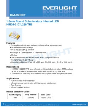
1. Ürün Genel Bakışı
HIR26-21C/L289/TR8, ultra küçük bir yüzey montaj cihazı (SMD) kızılötesi yayıcı diyottur. Kompakt, güvenilir kızılötesi ışık kaynağı gerektiren uygulamalar için tasarlanmış olup, modern otomatik montaj süreçleriyle uyumludur. Cihaz, ışık çıkışını optimize etmek için şeffaf plastik kılıf ve küresel üst lens ile 1.6 mm dairesel paket kullanır.
Temel avantajı, spektrumunun silikon fotodedektörlerle (fotodiyotlar ve fototransistörler) eşleşmesidir, bu da onu algılama sistemlerinde yüksek verimli kılar. Cihaz, bu dalga boyu aralığında yüksek performanslı kızılötesi yayıcılar için standart malzeme olan GaAlAs (galyum alüminyum arsenür) çip malzemesi kullanılarak üretilmiştir.
Hedef pazar, alanın kısıtlı olduğu ve güvenilir kızılötesi sinyal iletimi veya algılama gerektiren tüketici elektroniği, endüstriyel sensörler ve otomasyon ekipmanları için tasarımcılar ve üreticileri içerir.
2. Teknik Parametrelerin Detaylı Açıklaması
2.1 Mutlak Maksimum Değerler
Bu değerler, cihazda kalıcı hasara yol açabilecek limitleri tanımlar. Bu limitlerin ötesinde çalıştırılması önerilmez.
- Sürekli İleri Yön Akımı (IF)): 65 mA. Bu, ortam sıcaklığının (Ta) 25°C olduğu durumda sürekli olarak uygulanabilecek maksimum doğru akımdır.
- Tepe İleri Yön Akımı (IFP)): 1.0 A. Bu yüksek akım yalnızca darbe genişliği ≤100μs ve görev döngüsü ≤%1 olan darbe koşullarında izin verilir. Bu genellikle kısa, yüksek güçlü darbeler gerektiren uzaktan kumanda uygulamalarında kullanılır.
- Ters Gerilim (VR)): 5 V. Bu ters öngerilim voltajının aşılması, eklem delinmesine neden olabilir.
- Çalışma Sıcaklığı (Topr)): -40°C ila +85°C. Bu cihaz endüstriyel sıcaklık aralığı için uygundur.
- Depolama Sıcaklığı (Tstg)): -40°C ila +100°C.
- Lehimleme Sıcaklığı (Tsol)):260°C, süresi 5 saniyeyi geçmemek üzere, kurşunsuz geri akış işlemiyle uyumludur.
- Güç Tüketimi (Pd)):25°C veya altındaki serbest hava sıcaklığında 130 mW. Bu değer, elektrik gücü dönüşümünü ve cihazın ısı dağıtma kapasitesini dikkate alır.
2.2 Optoelektronik Özellikler
Bu parametreler Ta=25°C'de ölçülmüş olup, cihazın tipik çalışma koşullarındaki performansını tanımlar.
- Radyasyon Yoğunluğu (Ie)):Birim katı açı (steradyan) başına ışık gücü çıkışı. 20mA ileri akımda tipik değer 17 mW/sr'dir (minimum 10 mW/sr). Darbe koşullarında (100mA, ≤100μs, görev döngüsü ≤%1), tipik radyasyon yoğunluğu önemli ölçüde artarak 85 mW/sr'ye ulaşır ve darbe işleminin tepe çıkışı üzerindeki avantajını vurgular.
- Tepe Dalga Boyu (λp)): 850 nm (tipik değer). Bu, kızılötesi spektrumun yakın bölgesine aittir, silikon tabanlı dedektörler için çok uygundur ve 940 nm gibi daha kısa dalga boylarına kıyasla insan gözü için daha az görünürken, hala iyi bir atmosferik geçirgenliğe sahiptir.
- Spektral bant genişliği (Δλ)): 30 nm (tipik değer). Bu, tepe dalga boyu merkezli olarak yayılan dalga boyu aralığını tanımlar.
- İleri yönlü voltaj (VF)): 20mA'de, tipik ileri voltaj 1.40V'dir (aralık 1.20V ila 1.70V). 100mA darbe akımında, VFtipik olarak 1.60V'ye yükselir (aralık 1.40V ila 2.20V). Bu bilgi, sürücü devre tasarımı ve güç kaynağı seçimi için çok önemlidir.
- Ters yönlü akım (IR)): 5V ters voltajda maksimum 10 μA, iyi bir eklem kalitesini gösterir.
- Görüş açısı (2θ1/2)): 25 derece (tipik değer). Bu, radyasyon yoğunluğunun tepe (eksenel) değerinin yarısına düştüğü tam açıdır. 25° açı, yönlü algılama veya sinyal iletimi için uygun nispeten odaklanmış bir ışın sağlar.
3. Performans Eğrisi Analizi
Veri sayfası, bileşenin farklı koşullar altındaki davranışını anlamak için birkaç önemli grafik sağlar.
3.1 İleri Akım ile Ortam Sıcaklığı Arasındaki İlişki
Bu eğri, maksimum izin verilen sürekli ileri akımın, ortam sıcaklığı 25°C'yi aştıkça nasıl azaldığını gösterir. Aşırı ısınmayı önlemek için, sıcaklık maksimum çalışma sınırı olan 85°C'ye yaklaştıkça akım doğrusal olarak azaltılmalıdır. Tasarımcılar, uygulamalarının termal ortamında güvenilir çalışmayı sağlamak için bu grafiği kullanmalıdır.
3.2 Spektral Dağılım
Bu grafik, göreceli radyasyon yoğunluğunu dalga boyuna karşı çizerek, 850nm tepe noktasını ve yaklaşık 30nm'lik spektral bant genişliğini görsel olarak doğrular. Cihazın, belirtilen dalga boyu merkezli nispeten saf bir kızılötesi ışık yaydığını gösterir.
3.3 İleri Akım ile İleri Gerilim Arasındaki İlişki (I-V Eğrisi)
Bu temel karakteristik eğrisi, diyottaki akım ile voltaj arasındaki üstel ilişkiyi gösterir. Çalışma noktasını belirlemek ve akım sınırlama devreleri tasarlamak için çok önemlidir. Bu eğri sıcaklıkla birlikte kayar.
3.4 Radyasyon Şiddeti ile İleri Akım Arasındaki İlişki
Bu grafik, ışık çıkışını sürücü akımının bir fonksiyonu olarak gösterir. Genellikle doğrusal altı bir ilişki sergiler; çok yüksek akımlarda, termal etkiler ve diğer etkiler nedeniyle verimlilik (mA başına radyasyon yoğunluğu) düşebilir. Bu grafik, istenen ışık çıkış seviyesi için sürücü akımını optimize etmeye yardımcı olur.
3.5 Bağıl Radyasyon Şiddeti ile Açısal Yer Değiştirme İlişkisi
Bu kutupsal grafik, LED'in görüş açısını ve radyasyon modelini görsel olarak temsil eder. Gözlem açısı merkez eksenden (0°) saptıkça yoğunluğun, yaklaşık ±12.5°'de %50'ye düşerek (25° tam görüş açısını doğrulayarak) nasıl azaldığını gösterir. Bu, optik sistem tasarımı, hizalama ve yayılan ışığın kapsama alanını anlamak için çok önemlidir.
4. Mekanik ve Paketleme Bilgileri
4.1 Paket Boyutları
Bu cihaz, çift uçlu bir SMD paketidir ve gövde çapı 1.6 mm'dir. Veri sayfasındaki detaylı mekanik çizim, toplam yükseklik, bacak aralığı ve lens geometrisi dahil tüm kritik boyutları sağlar. Aksi belirtilmedikçe, tüm boyutlar milimetre cinsindendir ve standart tolerans ±0.1 mm'dir.
4.2 Pad Tasarımı ve Stencil Önerileri
Güvenilir lehimleme ve lehim topu gibi sorunlardan kaçınmak için önerilen pad yerleşimi ve stencil tasarımı sağlanmıştır. Temel öneriler şunları içerir:
- Lehim Pastası: Sn/Ag3.0/Cu0.5 (yaygın bir kurşunsuz alaşım).
- Şablon Kalınlığı: 0.10mm.
- Şablon açıklık deseni, küçük pedlerdeki lehim pastası hacmini kontrol etmek için tasarlanmış bir desen göstermektedir.
Önemli Not: Önerilen ped boyutları yalnızca referans içindir. Nihai PCB ped deseni, spesifik üretim sürecine, termal gereksinimlere ve bireysel tasarım ihtiyaçlarına göre değiştirilmelidir.
4.3 Polarite İşareti
Katot genellikle paket üzerindeki bir çentik, düz kenar veya tabandaki yeşil işaret gibi görsel işaretlerle belirtilir. Veri sayfası çizimleri, doğru PCB yönlendirmesi için kritik olan katot tarafını açıkça tanımlar.
5. Lehimleme ve Montaj Kılavuzu
5.1 Nem Hassasiyeti ve Depolama
Bu cihaz neme karşı hassastır. "Patlamış mısır" etkisini (reflow sırasında buharın hızlı genleşmesi nedeniyle paket çatlaması) önlemek için önlemler alınmalıdır.
- Kullanıma hazır olana kadar nem koruma torbasını açmayın.
- Açıldıktan sonra, ≤30°C sıcaklıkta ve ≤%60 bağıl nemde (RH) saklayın.
- Torba açıldıktan sonraki 168 saat (7 gün) içinde kullanın.
- Depolama süresi aşılırsa veya nem göstergesi nem girişini işaret ederse, bileşeni kullanmadan önce 60 ±5°C'de 24 saat boyunca ısıtın.
5.2 Reflow Lehimleme Süreci
Bu cihaz, kızılötesi ve buhar fazı reflow işlemleriyle uyumludur. Kurşunsuz reflow sıcaklık profili veri sayfasında önerilmiştir. Kritik parametreler ön ısıtma, ısı dengeleme, reflow tepe sıcaklığı (260°C'yi aşmamalı, süre ≤5 saniye) ve soğutma hızını içerir. Bileşenlere uygulanan termal stresi en aza indirmek için reflow işlemi iki defadan fazla uygulanmamalıdır.
5.3 El Lehimleme ve Tamir
El lehimleme yapılması gerekiyorsa, son derece dikkatli olunmalıdır:
- 使用烙铁头温度<350°C的烙铁。
- 每个端子接触时间限制在≤3秒。Gücü 25W veya daha düşük olan bir havya kullanın.
- Isı birikimini önlemek için her bir terminalin lehimlenmesi arasında ≥2 saniye ara verin.
- İlk lehimlemeden sonra onarım yapılması önerilmez. Kaçınılmazsa, lehim noktalarının ve LED'in kendisinin mekanik gerilime maruz kalmasını önlemek için çıkarma işleminde her iki terminali aynı anda ısıtmak için çift uçlu bir havya kullanın. Herhangi bir onarım işleminden sonra mutlaka cihaz fonksiyonunu doğrulayın.
5.4 Devre Kartı İşleme
Isıtma (lehimleme) işlemi sırasında LED'e mekanik stres uygulamaktan kaçının, lehimlemeden sonra devre kartını bükmeyin, çünkü bu bileşenin veya lehim bağlantılarının çatlamasına neden olabilir.
6. Paketleme ve Sipariş Bilgileri
6.1 Şeritleme ve Makara Özellikleri
Bu cihaz, endüstri standardı 7 inç çapındaki makaralarda, embosslu taşıyıcı şerit formunda sunulmaktadır. Taşıyıcı şerit boyutlarına (cep boyutu, aralık vb.) ilişkin detaylı çizimler sağlanmıştır. Her makara 1500 adet içerir.
6.2 Etiket Özellikleri
Makara etiketi, izlenebilirlik ve üretim için standart bilgileri içerir:
- CPN (Müşteri Parça Numarası)
- P/N (Üretici Parça Numarası: HIR26-21C/L289/TR8)
- ADET (Miktar)
- KAT (Sınıf/Kademe)
- RENK (Tepe Dalga Boyu)
- REF (Referans)
- LOT No. (Parti Numarası)
- MSL-X (Nem Duyarlılık Seviyesi)
- Made In (Üretildiği Ülke)
7. Uygulama Önerileri
7.1 Tipik Uygulama Senaryoları
- PCB'ye Monte Kızılötesi Sensör: Yakınlık Algılama, Nesne Tespiti, Robotlarda Hat Takibi.
- Kızılötesi Uzaktan Kumanda ÜnitesiStandart uzaktan kumanda LED'lerinden daha yüksek çıkış gücü gerektiren, parlak ortamlarda daha uzun mesafe veya daha iyi performans sağlaması muhtemel uygulamalar için uygundur.
- Gaz Sayacı/SayaçGenellikle kamu hizmeti sayaçları içindeki optik algılama mekanizmalarında kullanılır.
- Genel Amaçlı Kızılötesi SistemVeri iletimi, kodlama veya algılama için kompakt, güvenilir bir kızılötesi ışık kaynağı gerektiren herhangi bir gömülü sistem.
7.2 Tasarım Hususları
- Akım sınırlandırılmalıdır"Önemli Hususlar" bölümünde açıkça belirtildiği gibi, LED ile seri olarak harici bir akım sınırlama direnci (veya sabit akım sürücüsü) kullanılmalıdır. İleri voltajın bir aralığı vardır ve doğru şekilde sınırlanmazsa, güç kaynağı voltajındaki hafif bir artış, akımda büyük ve yıkıcı bir artışa neden olabilir.
- Termal YönetimGüç tüketimini (Pd=VF*IF) ve maksimum akımın sıcaklıkla azaltılmasını (derating) göz önünde bulundurun. Özellikle yüksek ortam sıcaklıklarında veya yüksek görev döngülü darbe uygulamalarında, yeterli PCB bakır alanı veya başka soğutma yöntemleri olduğundan emin olun.
- Optik Tasarım25° görüş açısı yönlülük sağlar. Daha geniş bir kapsama alanı için ikincil optik elemanlara (difüzör) ihtiyaç duyulabilir. Daha uzun mesafeler için ışın hüzmelerini paralel hale getirmek (kollime etmek) üzere lensler kullanılabilir.
- Sürücü Devresi1A'lik darbe işlemi için transistör veya MOSFET anahtarı gereklidir. Sürücünün tepe akımını ve gerekli hızlı yükselme/düşme sürelerini işleyebildiğinden emin olun.
8. Teknik Karşılaştırma ve Farklılıklar
Standart 5mm veya 3mm delikli kızılötesi LED'lere kıyasla, HIR26-21C/L289/TR8 belirgin avantajlara sahiptir:
- Boyut1.6mm SMD paketi, nihai ürünün küçültülmesini sağlar ve yüksek hızlı yüzey montajı ile uyumludur.
- Performans20mA'de tipik 17 mW/sr ışınım şiddeti rekabetçiyken, darbe koşullarında 85 mW/sr yüksek çıkış gereksinimleri için kritik bir özelliktir.
- Güvenilirlik: SMD yapısı ve standart reflow işlemiyle uyumluluğu, elle lehimlenmiş delikli bileşenlere kıyasla daha sağlam ve tutarlı lehim bağlantıları sağlar.
- Uygunluk:该器件无铅,符合RoHS、REACH标准,且无卤素(Br <900ppm,Cl <900ppm,Br+Cl <1500ppm),满足全球市场的严格环保法规。
9. Sıkça Sorulan Sorular (Teknik Parametrelere Dayalı)
9.1 Bu LED'i doğrudan 3.3V veya 5V mikrodenetleyici pini ile sürebilir miyim?
Hayır.Tipik ileri voltajı sadece 1.4V-1.6V'dir. Akım sınırlayıcı direnç kullanmadan doğrudan 3.3V veya 5V güç kaynağına bağlanırsa, aşırı akım nedeniyle LED neredeyse kesinlikle hasar görür. Seri bir direnç kullanmak şarttır ve bu direnç Ohm Kanunu'na göre hesaplanmalıdır: R = (VGüç Kaynağı- VF) / IF.
9.2 20mA DC anma değeri ile 100mA darbe anma değeri arasındaki fark nedir?
20mA anma değeri,sürekliçalışma için geçerlidir. 100mA anma değeri çok kısa sürelidarbe(≤100μs) ve düşük görev döngüsünde (≤%1). Bu, LED'in ortalama güç hala düşük olduğu için aşırı ısınmadan, daha kısa sürede daha güçlü sürülerek daha parlak bir flaş (85 mW/sr'ye karşı 17 mW/sr) üretmesini sağlar. Bu, uzaktan kumandalar için çok uygundur.
9.3 25 derecelik "görüş açısı" nasıl anlaşılır?
Bu, ışık şiddetinin maksimum değerinin (eksenel) yarısına düştüğü全açıdır. Bunu ana "ışın" veya ışık lobunun genişliği olarak düşünebilirsiniz. Bu açının ötesinde hala ışık yayılımı vardır, ancak şiddeti daha düşüktür. 25° açı orta derecede odaklanmıştır.
9.4 Nem hassasiyeti ve kızartma neden önemlidir?
Plastik SMD paketleri havadan nem emer. Yüksek sıcaklıktaki reflow lehimleme işlemi sırasında bu nem hızla buhara dönüşerek iç basınç oluşturur ve paketin çatlamasına veya çip ile tabakalaşmasına ("patlamış mısır" efekti) yol açabilir. Depolama ve ön ısıtma kurallarına uymak bu arıza modunu önler.
10. Pratik Tasarım ve Kullanım Örnekleri
Senaryo: Uzun Mesafeli Bir Kızılötesi İşaretçi (Beacon) Tasarımı
Tasarımcı, kapalı mekan ortamında ve bir miktar ortam kızılötesi gürültüsü varlığında, 20 metre uzaktaki bir sensör tarafından tespit edilebilen, kompakt, pil ile çalışan bir işaretçiye ihtiyaç duymaktadır.
- Sürüş yöntemi seçimi: Maksimum tespit mesafesi için, tasarımcı 85 mW/sr'ye varan darbe ışınım şiddetinden yararlanmak üzere darbe modu çalışmayı seçmiştir.
- Devre tasarımı: Mikrodenetleyici GPIO pini, bir N-kanal MOSFET'i kontrol eder. LED, bir güç kaynağı (örneğin 3.3V) ile MOSFET'in drenaj ucu arasına bir akım sınırlama direnci ile seri olarak bağlanır. Direnç değeri 100mA için hesaplanır: R = (3.3V - 1.6V) / 0.1A = 17Ω (18Ω standart değeri kullanılır). Mikrodenetleyici, genişliği 100μs ve görev döngüsü %1 olan (örneğin, 100μs açık, 9900μs kapalı) darbe üretir.
- PCB yerleşimiÖnerilen pad yerleşimini başlangıç noktası olarak alın. Yüksek akım darbeleri sırasında ısı dağılımına yardımcı olmak için padlerin etrafına ek termal padler ve bakır döküm (copper pour) ekleyin.
- MontajBileşenleri PCB üzerine yerleştirin. LED makaralarını uygun şekilde depolayın, monte edilmiş kartı önerilen kurşunsuz profil ile bir kez reflow lehimleyin.
- Optik (İsteğe Bağlı)Mesafeyi daha da artırmak için, LED'in üzerine ışın hüzmesini daraltmak ve çıkış gücünü hedef mesafedeki daha küçük bir alana yoğunlaştırmak için basit bir plastik kolimatör lens yerleştirilebilir.
Bu vaka çalışması, kilit veri sayfası parametrelerinin – darbe ışınım şiddeti, ileri yönlü voltaj, akım değerleri ve paket boyutları – pratik tasarımı nasıl doğrudan yönlendirdiğini göstermektedir.
11. Çalışma Prensibi
Kızılötesi Işık Yayan Diyot (IR LED), bir yarı iletken p-n eklemindeki elektrolüminesans prensibiyle çalışır. İleri yönlü bir voltaj uygulandığında, n-tipi malzemeden elektronlar ve p-tipi malzemeden delikler (hole'lar) eklem bölgesine enjekte edilir. Bu taşıyıcılar yeniden birleştiğinde enerji açığa çıkarır. GaAlAs diyotlarında olduğu gibi, yarı iletken malzemenin enerji bant aralığı, açığa çıkan enerjinin kızılötesi spektrumda, yaklaşık 850 nanometre gibi belirli bir dalga boyuna karşılık gelen fotonlara denk gelmesi için tasarlanmıştır. Şeffaf epoksi kılıf, yayılan ışığı belirtilen ışınım modeline (25° yarı güç açısı) şekillendiren bir lens görevi görür.
12. Sektör Eğilimleri ve Gelişmeler
Ultra küçük kızılötesi LED pazarı gelişmeye devam ediyor. HIR26-21C/L289/TR8 gibi cihazlarla ilişkili temel trendler şunları içerir:
- Artan Entegrasyon: Trend, sensör modüllerini basitleştirmek için kızılötesi vericileri sürücü IC'leri ve hatta fotodedektörlerle tek bir pakette entegre etmektir.
- Daha Yüksek Verimlilik: Devam eden malzeme bilimi araştırmaları, kızılötesi LED'lerin duvar verimliliğini (ışık güç çıkışı / elektrik güç girişi) artırmayı, böylece aynı boyuttaki paketlerde daha düşük güç tüketimi veya daha yüksek çıkış elde etmeyi amaçlamaktadır.
- Yeni Dalga Boyları: 850nm ve 940nm baskın olsa da, gaz algılama veya göz güvenliğinin artırılması gibi belirli uygulamalar için diğer kızılötesi dalga boylarına olan ilgi artıyor.
- Gelişmiş Paketleme: Boyut ve maliyeti daha da azaltırken termal performansı artırmak için Çip Ölçekli Paketleme (CSP) ve Wafer Seviyesi Paketleme geliştirilmesi.
- Uygulama Genişlemesi:
- Biyometrik ve Güvenlik: Yüz tanıma, iris tarama.
- OtomotivAraç içi yolcu algılama, sürücü izleme sistemi.
- Tüketici ElektroniğiTelefon/tablet yakınlık algılama, hareket tanıma.
- Endüstriyel Nesnelerin İnternetiMakine görüşü, durum izleme.
HIR26-21C/L289/TR8 gibi bileşenler, küçük boyutları, güvenilir performansları ve çevre dostu standartlara uyumları sayesinde, kompakt ve verimli kızılötesi ışık kaynaklarının temel bir gereklilik olduğu bu genişleyen pazarlara hizmet etmek için ideal bir seçenektir.
LED Özellik Terimlerinin Ayrıntılı Açıklaması
LED Teknik Terimlerinin Tam Açıklaması
I. Optoelektronik Performans Temel Göstergeleri
| Terim | Birim/Gösterim | Basit Açıklama | Neden Önemli |
|---|---|---|---|
| Işık Verimliliği (Luminous Efficacy) | lm/W (lümen/vat) | Bir vat elektrik enerjisi başına üretilen ışık akısı miktarıdır, değer ne kadar yüksekse enerji tasarrufu o kadar fazladır. | Aydınlatma armatürünün enerji verimliliği sınıfını ve elektrik maliyetini doğrudan belirler. |
| Işık Akısı (Luminous Flux) | lm (lümen) | Bir ışık kaynağı tarafından yayılan toplam ışık miktarıdır, halk arasında "parlaklık" olarak adlandırılır. | Bir armatürün yeterince parlak olup olmadığını belirler. |
| Işık Açısı (Viewing Angle) | ° (derece), örn. 120° | Işık şiddetinin yarıya düştüğü açı, ışık hüzmesinin genişliğini veya darlığını belirler. | Aydınlatma alanını ve düzgünlüğünü etkiler. |
| Renk Sıcaklığı (CCT) | K (Kelvin), örn. 2700K/6500K | Işığın sıcak veya soğuk rengi; düşük değer sarı/sıcak, yüksek değer beyaz/soğuk eğilimlidir. | Aydınlatma atmosferini ve uygun kullanım senaryolarını belirler. |
| Renksel Geriverim İndeksi (CRI / Ra) | Birimsiz, 0–100 | Işık kaynağının nesnelerin gerçek rengini yansıtma yeteneği; Ra≥80 tercih edilir. | Renk gerçekliğini etkiler; alışveriş merkezleri, sanat galerileri gibi yüksek gereksinimli mekanlarda kullanılır. |
| Renk toleransı (SDCM) | MacAdam elips adım sayısı, örn. "5-step" | Renk tutarlılığının nicel göstergesi, adım sayısı ne kadar küçükse renk tutarlılığı o kadar yüksektir. | Aynı parti aydınlatma armatürlerinin renklerinin farklılık göstermemesini garanti eder. |
| Baskın dalga boyu (Dominant Wavelength) | nm (nanometre), örn. 620nm (kırmızı) | Renkli LED'lerin rengine karşılık gelen dalga boyu değeri. | Kırmızı, sarı, yeşil gibi tek renkli LED'lerin renk tonunu belirler. |
| Spektral Dağılım (Spectral Distribution) | Dalga Boyu vs. Şiddet Eğrisi | LED'in yaydığı ışığın farklı dalga boylarındaki şiddet dağılımını gösterir. | Renksel geriverim ve renk kalitesini etkiler. |
II. Elektriksel Parametreler
| Terim | Sembol | Basit Açıklama | Tasarım Hususları |
|---|---|---|---|
| İleri Yönlü Gerilim (Forward Voltage) | Vf | LED'in yanması için gereken minimum voltaj, "başlangıç eşiği" gibi. | Sürücü güç kaynağı voltajı ≥Vf olmalıdır, birden fazla LED seri bağlandığında voltajlar toplanır. |
| İleri Yön Akımı (Forward Current) | If | LED'in normal şekilde ışık yaymasını sağlayan akım değeri. | Genellikle sabit akım sürücü kullanılır, akım parlaklığı ve ömrü belirler. |
| Maksimum Darbe Akımı (Pulse Current) | Ifp | Kısa süreliğe dayanabilen tepe akımı, karartma veya flaş için kullanılır. | Darbe genişliği ve görev döngüsü sıkı kontrol edilmelidir, aksi takdirde aşırı ısınma ve hasar oluşur. |
| Ters Gerilim (Reverse Voltage) | Vr | LED'nin dayanabileceği maksimum ters voltaj, aşılırsa delinme meydana gelebilir. | Devrede ters bağlantı veya voltaj darbelerinin önlenmesi gerekir. |
| Thermal Resistance | Rth(°C/W) | Isının çipten lehim noktasına iletilmesindeki direnç, değer ne kadar düşükse soğutma o kadar iyidir. | Yüksek termal direnç daha güçlü bir soğutma tasarımı gerektirir, aksi takdirde bağlantı sıcaklığı yükselir. |
| Elektrostatik Deşarj Direnci (ESD Immunity) | V (HBM), örneğin 1000V | Elektrostatik darbe direnci, değer ne kadar yüksekse elektrostatik hasara karşı o kadar dayanıklıdır. | Üretimde, özellikle yüksek hassasiyetli LED'ler için elektrostatik koruma önlemleri alınmalıdır. |
Üç. Termal Yönetim ve Güvenilirlik
| Terim | Kritik Göstergeler | Basit Açıklama | Etki |
|---|---|---|---|
| Kavşak Sıcaklığı (Junction Temperature) | Tj (°C) | LED çipinin içindeki gerçek çalışma sıcaklığı. | Her 10°C düşüşte ömür iki katına çıkabilir; aşırı yüksek sıcaklık ışık azalmasına ve renk kaymasına yol açar. |
| Işık Azalması (Lumen Depreciation) | L70 / L80 (saat) | Parlaklığın başlangıç değerinin %70'ine veya %80'ine düşmesi için gereken süre. | LED'in "kullanım ömrünü" doğrudan tanımlar. |
| Lümen Bakım Oranı (Lumen Maintenance) | % (örneğin %70) | Belirli bir kullanım süresinden sonra kalan parlaklığın yüzdesi. | Uzun süreli kullanım sonrası parlaklık koruma yeteneğini karakterize eder. |
| Renk Kayması (Color Shift) | Δu′v′ veya MacAdam Elipsi | Kullanım sürecindeki renk değişim derecesi. | Aydınlatma sahnesinin renk tutarlılığını etkiler. |
| Termal Yaşlandırma (Thermal Aging) | Malzeme performansında düşüş | Uzun süreli yüksek sıcaklığa bağlı olarak paketleme malzemesinde bozulma. | Parlaklıkta azalma, renk değişimi veya açık devre arızasına yol açabilir. |
D. Paketleme ve Malzemeler
| Terim | Yaygın Tipler | Basit Açıklama | Özellikler ve Uygulamalar |
|---|---|---|---|
| Paket Tipi | EMC, PPA, Seramik | Çipi koruyan ve optik, termal arayüz sağlayan kasa malzemesi. | EMC ısıya dayanıklı ve düşük maliyetli; seramik ısı dağıtımı üstün ve uzun ömürlü. |
| Çip Yapısı | Düz Kurulum, Ters Çevirme (Flip Chip) | Çip elektrot düzenleme yöntemi. | Ters montaj daha iyi ısı dağıtımı, daha yüksek ışık verimliliği sağlar ve yüksek güç için uygundur. |
| Fosfor kaplama | YAG, silikat, nitrür | Mavi ışık yayan çip üzerine kaplanır, bir kısmı sarı/kırmızı ışığa dönüştürülerek beyaz ışık oluşturmak için karıştırılır. | Farklı fosforlar ışık verimliliğini, renk sıcaklığını ve renksel geriverimi etkiler. |
| Lens/Optik Tasarım | Düz, mikrolens, tam yansıma | Paketleme yüzeyindeki optik yapı, ışık dağılımını kontrol eder. | Işık açısını ve ışık dağılım eğrisini belirler. |
V. Kalite Kontrolü ve Sınıflandırma
| Terim | Sınıflandırma içeriği | Basit Açıklama | Amaç |
|---|---|---|---|
| Işık Akısı Sınıflandırması | Kodlar, örneğin 2G, 2H | Parlaklık seviyelerine göre gruplandırma, her grubun minimum/maksimum lümen değeri vardır. | Aynı parti ürünlerin parlaklık tutarlılığını sağlamak. |
| Gerilim Sınıflandırması | Kodlar örneğin 6W, 6X | İleri voltaj aralığına göre gruplandırma. | Sürücü güç kaynağı eşleştirmesini kolaylaştırır, sistem verimliliğini artırır. |
| Renk Sınıflandırması | 5-step MacAdam elipsi | Renk koordinatlarına göre gruplandırma, rengin çok dar bir aralıkta kalmasını sağlar. | Renk tutarlılığını sağlayın, aynı armatür içinde renk düzensizliğinden kaçının. |
| Renk sıcaklığı sınıflandırması | 2700K, 3000K vb. | Renk sıcaklığına göre gruplandırın, her grubun karşılık gelen bir koordinat aralığı vardır. | Farklı senaryoların renk sıcaklığı ihtiyaçlarını karşılayın. |
VI. Test ve Sertifikasyon
| Terim | Standart/Test | Basit Açıklama | Anlam |
|---|---|---|---|
| LM-80 | Lümen Bakım Testi | Sabit sıcaklık koşullarında uzun süre yakılarak parlaklık azalma verileri kaydedilir. | LED ömrünü tahmin etmek için kullanılır (TM-21 ile birlikte). |
| TM-21 | Ömür tahmin standardı | LM-80 verilerine dayanarak gerçek kullanım koşullarındaki ömrü hesaplar. | Bilimsel ömür tahmini sağlar. |
| IESNA standardı | Aydınlatma Mühendisliği Topluluğu standardı | Optik, elektrik ve termal test yöntemlerini kapsar. | Sektörde kabul görmüş test temeli. |
| RoHS / REACH | Çevre dostu sertifikasyon | Ürünün zararlı maddeler (kurşun, cıva gibi) içermemesini sağlar. | Uluslararası pazarlara giriş için erişim koşulu. |
| ENERGY STAR / DLC | Enerji verimliliği sertifikasyonu. | Aydınlatma ürünleri için enerji verimliliği ve performans sertifikasyonu. | Genellikle devlet alımları ve sübvansiyon programlarında kullanılır, piyasa rekabet gücünü artırır. |