İçindekiler
- 1. Ürün Genel Bakış
- 2. Teknik Parametrelerin Detaylı Açıklaması
- 2.1 Mutlak Maksimum Değerler
- 2.2 Optoelektronik Özellikler
- 2.2.1 Giriş Karakteristiği (LED Tarafı)
- 2.2.2 Çıkış Karakteristiği (Fototransistör Tarafı)
- 2.2.3 Transfer Karakteristiği
- 3. Performans Eğrisi Analizi
- 4. Mekanik ve Paketleme Bilgileri
- 4.1 Paketleme Seçenekleri ve Boyutlar
- 4.2 Pin Konfigürasyonu ve Polarite
- 4.3 Önerilen PCB Lehim Pedi Yerleşimi
- 5. Lehimleme ve Montaj Kılavuzu
- 6. Paketleme ve Sipariş Bilgileri
- 7. Uygulama Önerileri
- 7.1 Tipik Uygulama Senaryoları
- 7.2 Tasarım Dikkat Edilmesi Gerekenler
- 8. Teknik Karşılaştırma ve Konumlandırma
- 9. Sıkça Sorulan Sorular (Teknik Parametrelere Dayalı)
- 10. Gerçek Tasarım Örnekleri
- 11. Çalışma Prensibi
- 12. Teknoloji Trendleri
1. Ürün Genel Bakış
EL2514-G serisi, yüksek performanslı 4 pinli Çift Sıralı Düz Paket (DIP) fototransistör tipi optokuplörlerdir. Bu cihazlar, iki devre arasında güvenilir elektriksel izolasyon ve sinyal iletimi sağlamak üzere tasarlanmıştır. Temel bileşeni, bir silikon fototransistör dedektörüne optik olarak bağlanan bir kızılötesi ışık yayan diyottur. EL2514-G'nin önemli bir tasarım özelliği, yük direnci kiloohm seviyelerinde olsa bile elde edilebilen nispeten yüksek anahtarlama hızı için optimize edilmiş olmasıdır. Bu, hem izolasyon hem de orta bant genişliği gerektiren uygulamalar için uygun kılar.
Bu seri, katı çevre ve güvenlik standartlarına uygunluğu ile karakterize edilir. Halojensiz bir süreçle üretilmiştir ve brom (Br) ile klor (Cl) içeriği belirli sınır değerlere uygundur. Ayrıca, UL, cUL, VDE, SEMKO, NEMKO, DEMKO, FIMKO ve CQC gibi önde gelen uluslararası güvenlik kuruluşlarından sertifikasyon almıştır; bu da küresel pazarlar ve düzenlemeli uygulamalar için uygunluğunu garanti eder.
2. Teknik Parametrelerin Detaylı Açıklaması
2.1 Mutlak Maksimum Değerler
Bu cihaz, belirtilen sınırlar içinde güvenilir çalışacak şekilde tasarlanmıştır. Bu mutlak maksimum değerlerin aşılması kalıcı hasara neden olabilir. Kritik değerler şunları içerir: Giriş LED'in sürekli ileri akımı (IF) 50 mA'dir, 1µs darbe için tepe ileri akımı (IFP) 0.5 A, ters voltaj (VR) 6 V'dir. Çıkış tarafında, kollektör akımı (IC) nominal değeri 20 mA, kollektör-emitör voltajı (VCEO) 40 V'dir. Cihazın toplam güç tüketimi (PTOT) 200 mW'dır. Kritik bir güvenlik parametresi izolasyon voltajıdır (VISO) 5000 V'dirrmsBelirli nem koşullarında (%40-60 RH), giriş ve çıkış pinleri kısa devre yapılarak 1 dakika test edilir. Çalışma sıcaklığı aralığı geniştir, -55°C ila +110°C arasındadır.
2.2 Optoelektronik Özellikler
Bu parametreler, cihazın 25°C normal çalışma koşullarındaki performansını tanımlar.
2.2.1 Giriş Karakteristiği (LED Tarafı)
- İleri Yönlü Gerilim (VF):Tipik değer 1.2 V'dur, IF= 20 mA sürüldüğünde maksimum 1.4 V'dur. Bu, sürücü devresinin besleme voltajının tasarımı için çok önemlidir.
- Ters akım (IR):VR= 4V'de maksimum 10 µA, iyi diyot karakteristiğini gösterir.
- Giriş kapasitansı (Cin):Tipik 30 pF'den maksimum 250 pF'ye kadar değişen bir aralıktır. Bu kapasitans, yüksek frekans sürüş kapasitesini etkiler.
2.2.2 Çıkış Karakteristiği (Fototransistör Tarafı)
- Kollektör-Emitör Karanlık Akımı (ICEO):LED kapalıyken ve VCE= 10V'de maksimum 100 nA. Bu düşük sızıntı akımı, iyi bir "kapalı" durum elde etmek için çok önemlidir.
- Kollektör-Emitör delinme gerilimi (BVCEO):Minimum 40 V, IC= 0.1 mA koşulunda ölçülür.
- Emitör-Kollektör delinme gerilimi (BVECO):Minimum değeri 0.45 V'dir, nispeten düşüktür ve fototransistörün asimetrisini gösterir.
2.2.3 Transfer Karakteristiği
- Akım Transfer Oranı (CTR):Bu, temel bir performans göstergesidir ve (IC/ IF) * %100 olarak tanımlanır. EL2514-G için, standart test koşullarında IF= 5 mA ve VCE5V altında, CTR aralığı %50 ila %200'dür. Bu geniş aralık, cihazlar arasındaki farklılıkları karşılamak için uygun devre tasarımı gerektirir.
- Kollektör-emitter doyum voltajı (VCE(sat)):IF= 5 mA ve IC= 0.4 mA'de maksimum 0.35 V'dir. Düşük doyum voltajı, güçlü bir mantıksal düşük seviye çıkışı elde etmeye olanak tanır.
- Yalıtım direnci (RIO):500 V'de10altında minimum 5 x 10DCΩ, mükemmel DC izolasyonu sağlar.
- Yüzer kapasitör (CIO):Tipik değer 0.6 pF, maksimum 1.0 pF'dir. Bu düşük kapasitans, ortak mod geçici bağışıklığını artırmaya yardımcı olur.
- Anahtarlama süresi:Vaçık) ve kapanma süresi (tkapalı) maksimum özellikleri 25 µs'dir. Bu, cihazın dijital sinyal iletimi için kullandığı hızı tanımlar.CC= 5V, IF= 5 mA, RL= 5 kΩ test koşullarında, açılma süresi (t
3. Performans Eğrisi Analizi
Veri sayfası tipik optoelektronik karakteristik eğrilerine atıfta bulunur. Sağlanan metinde belirli grafikler ayrıntılı olarak açıklanmasa da, bu tür eğriler genellikle temel parametreler arasındaki ilişkiyi gösterir. Tasarımcılar aşağıdakileri tanımlayan eğriler görmeyi beklemelidir:
- CTR'nin ileri akım (IF) ile ilişkisi:Akım transfer oranının farklı LED sürücü akımlarında nasıl değiştiğini gösterir.
- CTR'nin ortam sıcaklığı (TA) ile ilişkisi:CTR'nin sıcaklığa bağımlılığını açıklayın; genellikle sıcaklık arttıkça düşer.
- Kollektör akımı (IC) ile kollektör-emiter gerilimi (VCE) ile ilişkisi:Farklı LED akımları için eğri ailesi, fototransistörün çıkış karakteristiğini gösterir.
- Anahtar dalga formu:taçıkve tkapalıölçüm koşullarını tanımlamak için test devresi ve ilgili dalga formları (Şekil 7) sağlanmıştır. Bu genellikle bir LED'i süren bir darbe üreteci ve bir fototransistör çıkışını yük direnci üzerinde izleyen bir osiloskop içerir.
Bu eğrilerin analizi, beklenen çalışma sıcaklığı ve akım aralığında devre performansını optimize etmek için çok önemlidir.
4. Mekanik ve Paketleme Bilgileri
4.1 Paketleme Seçenekleri ve Boyutlar
EL2514-G, farklı montaj işlemlerine uyum sağlamak için çeşitli 4 pinli DIP paket varyantları sunar:
- Standart DIP:Klasik DIP (Doğrudan Takma) paketleme.
- Seçenek M:"Geniş Bacak Eğimi" özelliğine sahiptir, 0,4 inç (yaklaşık 10,16 mm) bacak aralığı sağlar; bu, belirli PCB düzenleri veya kaçak akım mesafesi gereksinimleri için yararlı olabilir.
- Seçenek S1:Düşük profilli bir yüzey montaj (SMD) bacak formudur. İki farklı şerit ambalaj seçeneği (TU, TD) sunar, her makara 1500 adet cihaz içerir.
- Seçenek S2:Yine düşük profilli başka bir yüzey montaj bacak formudur, şerit ambalaj seçeneği makara başına 2000 adet cihaz içerir.
Her bir paketleme türü için, gövde boyutları, bacak uzunluğu, bacak aralığı ve karttan yükseklik gibi kritik ölçüleri içeren detaylı boyut çizimleri sağlanmıştır. Giriş ve çıkış tarafı arasındaki sürünme mesafesi 7.62 mm'den büyük olarak belirlenmiştir, bu da yüksek izolasyon seviyesine ulaşılmasına yardımcı olur.
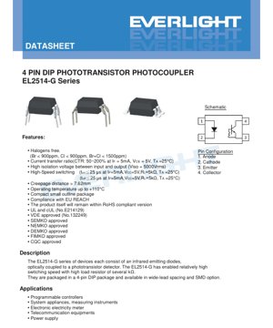
4.2 Pin Konfigürasyonu ve Polarite
Bu cihaz, standart 4 bacaklı DIP bacak düzeni kullanır:
- Pin 1: Anot (LED girişi)
- Pin 2: Katot (LED girişi)
- Pin 3: Emitör (Fototransistör çıkışı)
- Pin 4: Kollektör (Çıkış Fototransistörü)
4.3 Önerilen PCB Lehim Pedi Yerleşimi
Yüzey montaj seçenekleri (S1 ve S2) için veri sayfası, önerilen lehim padi yerleşimini sağlar. Bunlar, güvenilir lehimleme ve mekanik kararlılığı sağlamak için tasarlanmış referans tasarımlardır. Belge, bu boyutların özel üretim süreci ve gereksinimlerine (lehim macunu miktarı ve ısı dağıtımı dikkatleri gibi) göre değiştirilmesi gerektiğini açıkça belirtir.
5. Lehimleme ve Montaj Kılavuzu
Bu cihazın lehimleme sıcaklığı (TSOL) derecelendirmesi 260°C, en fazla 10 saniyedir. Bu, tipik kurşunsuz geri akış lehimleme eğrisiyle uyumludur. Dalga lehimleme için delikli montajda, paket gövdesinin maksimum sıcaklığını aşmamaya dikkat ederek standart endüstri uygulamaları izlenmelidir. Depolama sıcaklık aralığı -55°C ila +125°C'dir. SMD montajında kullanılıyorsa, cihazın nem korumalı ambalajda saklanması ve nem maruziyet seviyesi aşıldığında uygun kurutma prosedürlerinin takip edilmesi önerilir.
6. Paketleme ve Sipariş Bilgileri
Sipariş kodu aşağıdaki kalıba uyar: EL2514X(Y)-VG.
- X:Bacak formu seçenekleri (S1, S2, M veya standart DIP için boş bırakın).
- Y:Şerit Ambalaj Seçeneği (TU, TD veya tüp için boş bırakın).
- V:VDE güvenlik sertifikasyonunu belirtir (isteğe bağlı).
- G:Halojensiz yapıyı belirtir.
7. Uygulama Önerileri
7.1 Tipik Uygulama Senaryoları
EL2514-G, elektriksel izolasyon, gürültü bağışıklığı veya seviye dönüşümü gerektiren uygulamalar için çok uygundur. Bahsedilen spesifik uygulamalar şunları içerir:
- Programlanabilir Mantıksal Denetleyici (PLC):Dijital G/Ç modüllerini merkezi işlem birimi ve saha cihazlarından yalıtmak için kullanılır.
- Sistem Ekipmanları ve Ölçüm Cihazları:Endüstriyel ekipmanlarda sensör sinyallerini veya iletişim hatlarını izole etmek.
- Elektronik elektrik sayacı:Ölçüm devrelerinde güvenlik sağlamak ve gürültüyü bastırmak için izolasyon sağlamak.
- Telekomünikasyon ekipmanı:Veri hattı veya güç kaynağı geri besleme devresindeki sinyal izolasyonu.
- Güç Kaynağı:Genellikle anahtarlamalı güç kaynaklarının (SMPS) geri besleme devrelerinde, ikincil taraftaki geri besleme sinyalini birincil taraftaki denetleyiciden izole etmek için kullanılır; böylece güvenlik ve kararlılık artırılır.
7.2 Tasarım Dikkat Edilmesi Gerekenler
- CTR Değişimi:Alıcı devre tasarlanırken (örneğin, karşılaştırıcı eşik değeri, çekme direnci değeri), devrenin %50-200'lik tüm CTR aralığında güvenilir çalışması sağlanmalıdır.
- Hız ve Yük:Anahtarlama hızı 5 kΩ yük altında belirtilmiştir. Daha küçük bir yük direnci kullanmak genellikle anahtarlama hızını artırır, ancak çıkış salınımını azaltır ve güç tüketimini artırır. Daha büyük dirençler, özellikle fototransistörün depolama süresinden kaynaklanan kapanma süresini yavaşlatır.
- LED Akım Sınırlama:İleri yönlü akımın (I) önerilen çalışma aralığı (tipik 5-7 mA) içinde veya mutlak maksimum değerin altında kalmasını sağlamak için mutlaka seri bir direnç kullanın.FBu, uzun vadeli güvenilirlik ve kararlı bir CTR sağlar.
- Gürültü Bağışıklığı:Optokuplörler mükemmel ortak mod bastırma sağlasa da, doğru PCB düzeni için yüksek frekanslı gürültüyü bastırmak amacıyla giriş ve çıkış izlerini ayırarak ve cihaz bacakları yakınında bypass kapasitörleri kullanarak önlem alınmalıdır.
8. Teknik Karşılaştırma ve Konumlandırma
EL2514-G, temel özelliklerini birleştirerek pazarda öne çıkar. Yüksek izolasyon voltajı (5000 Vrms) ve uzun kaçak yolu, katı güvenlik gereksinimleri olan uygulamalar için onu güçlü bir aday yapar. Halojensiz yapısı, çevre düzenlemelerini ve müşterilerin "yeşil" elektronik tercihlerini karşılar. Kapsamlı sertifika portföyü (UL, VDE vb.), küresel pazarlar için nihai ürün sertifikasyon engellerini azaltır. Anahtarlama hızı (25 µs) birçok dijital izolasyon ve güç geri besleme uygulaması için uygun olsa da, nanosaniye seviyesinde anahtarlama süresi gerektiren veri iletişimi için ultra yüksek hızlı bir kuplör olarak konumlandırılmamıştır. Bu nedenle, EL2514-G en iyi şekilde, güvenilirlik, güvenlik uyumluluğu ve orta düzey performans için optimize edilmiş, sağlam, genel amaçlı bir optokuplör olarak görülmelidir.
9. Sıkça Sorulan Sorular (Teknik Parametrelere Dayalı)
Soru: CTR aralığı %50-200, devre tasarımım için ne anlama geliyor?
Cevap: Bu, çıkış akımının giriş akımının yarısı kadar düşük veya iki katı kadar yüksek olabileceği anlamına gelir. Devreniz her iki uç durumda da düzgün çalışmalıdır. Dijital arayüzler için bu, pull-up direnci seçimini ve sonraki kapı devrelerinin veya mikrodenetleyicilerin giriş eşiklerini etkiler.
Soru: LED'i doğrudan bir voltaj kaynağı ile sürebilir miyim?
Cevap: Hayır. LED'ler akım kontrollü cihazlardır. İstenen I'yi ayarlamak ve aşırı akım hasarını önlemek için, güç kaynağınızın voltajı tipik V ile uyumlu olsa bile, LED ile seri olarak her zaman bir akım sınırlama direnci kullanmalısınız.Fve aşırı akım hasarını önlemek için, güç kaynağınızın voltajı tipik V ile uyumlu olsa bile.F.
Soru: İzolasyon voltajı 5000 Vrms'tir. Bu, giriş ve çıkış arasına sürekli olarak 5000V uygulayabileceğim anlamına mı geliyor?
Cevap: Hayır. Bu, kontrollü koşullar altında bir dakika boyunca test edilen bir yalıtım direnci değeridir. Uygulamadaki sürekli çalışma voltajı bu değerin önemli ölçüde altında olmalıdır ve bu, ilgili güvenlik standartları tarafından tanımlanır.
Soru: S1 ve S2 seçenekleri arasındaki fark nedir?
Cevap: Temel fark, paket boyutu ve şerit boyutudur. S2'nin gövde genişliği (B0 boyutu) biraz daha büyüktür ve daha geniş bir şerit kullanır (S1 için 16mm, S2 için 24mm), her makara daha fazla cihaz alabilir (S1 için 1500 adet, S2 için 2000 adet). Seçim, PCB alan kısıtlamalarınıza ve montaj hattı besleyici uyumluluğunuza bağlıdır.
10. Gerçek Tasarım Örnekleri
Senaryo: Mikrodenetleyicinin dijital sinyalini yüksek gerilim bölümüne izole etmek.
Bir mikrodenetleyici (3.3V mantık), farklı ve gürültülü bir yüksek gerilim potansiyelinde çalışan bir devreye AÇIK/KAPALI sinyali göndermelidir. İzolasyon için EL2514-G kullanılabilir.
Tasarım Adımları:
- Giriş tarafı:Bir akım sınırlama direnci (RlimitMikrodenetleyici GPIO pinini optokuplörün anoduna bağlayın. R'yi hesaplayınlimit= (VCC_MCU- VF) / IF. V içinCC_MCU=3.3V, VF~1.2V, hedef IF=5mA ise, Rlimit= (3.3-1.2)/0.005 = 420Ω. Standart bir 470Ω direnç kullanın. Katodu toprağa bağlayın.
- Çıkış tarafı:Kollektörü, izole yüksek voltajlı güç kaynağına (örneğin 12V) bağlı bir çekme direncine (RL) bağlayın. Emitörü izole toprağa bağlayın. RLDeğeri hızı ve akımı etkiler. Veri sayfasındaki test koşullarında belirtilen 5kΩ direnç, belirtilen anahtarlama sürelerini sağlar. Ardından, kollektör düğümünden gelen sinyal, izolasyon tarafındaki bir MOSFET kapısını veya başka bir mantık girişini sürebilir.
- Düzen:Giriş ve çıkış bölümlerini PCB üzerinde fiziksel olarak ayırın. Paket yeteneklerine bağlı olarak 7.62 mm'den fazla kaçak akım mesafesini koruyun. Bağlayıcının her iki tarafındaki güç ve toprak arasına, cihaz bacaklarına yakın küçük bir bypass kapasitörü (örneğin 0.1µF) yerleştirin.
11. Çalışma Prensibi
Optokuplör, iki izole devre arasında elektrik sinyallerini iletmek için ışığı kullanan bir cihazdır. EL2514-G'de, giriş pinlerine (1 ve 2) uygulanan akım, kızılötesi ışık yayan diyotun (LED) foton yaymasını sağlar. Bu fotonlar, şeffaf bir yalıtım boşluğundan (genellikle kalıp bileşikten yapılmış) geçer ve çıkış tarafındaki (pin 3 ve 4) bir silikon fototransistörün taban bölgesine çarpar. Gelen ışık, taban bölgesinde elektron-boşluk çiftleri oluşturarak etkin bir şekilde taban akımı görevi görür. Daha sonra, bu fotovoltaik taban akımı transistörün kazancı ile yükseltilerek, giriş LED akımı (IC) ile orantılı bir kollektör akımı (IF) üretir. Oran IC/IFBu, akım transfer oranıdır (CTR). Kritik nokta, giriş ve çıkış arasındaki tek bağlantının ışık huzmesi olması ve böylece elektriksel izolasyon sağlamasıdır.
12. Teknoloji Trendleri
Optokuplör pazarı sürekli gelişmektedir. EL2514-G gibi cihazları etkileyen trendler şunları içerir:
- Entegrasyon Yoğunluğunun Artırılması:Birden fazla izolasyon kanalının tek bir pakette birleştirilmesi veya kapı sürücüsü, hata yükseltici gibi ek işlevlerin entegre edilmesi.
- Mbps veri hızlarında dijital iletişim protokollerini (USB, CAN, RS-485) desteklemek için, entegre yükselticili fotodiyot gibi daha hızlı dedektörler kullanan kuplörlerin geliştirilmesi.Güvenilirliği ve Ömrü Artırma:
- CTR'nin uzun vadeli kararlılığını artırmaya odaklanın; CTR, LED'in yaşlanması (özellikle yüksek sıcaklık ve yüksek akım altında) nedeniyle zamanla bozulur.Daha Sıkı Çevresel Uyumluluk:
- RoHS ve halojensiz olmanın ötesinde, tedarik zincirinde PFAS gibi maddelere ve daha geniş sürdürülebilirlik göstergelerine yönelik artan bir odaklanma var.Alternatif izolasyon teknolojileri:
- Optokuplörler birçok uygulamada hâlâ baskın olsa da, kapasitif izolasyon (SiObariyer) ve manyetik izolasyon (transformatör kullanarak) gibi teknolojiler, çok yüksek hız, düşük güç tüketimi veya yüksek entegrasyon yoğunluğu gerektiren alanlarda rekabet ediyor. Optokuplörler, basitlik, yüksek ortak mod geçici bağışıklığı (CMTI) ve olgun güvenlik sertifikasyonları konularında avantajlarını koruyor.2EL2514-G, güvenlik sertifikasyonu, çevresel uyumluluk ve sağlam performansa odaklanarak, endüstriyel, enerji ve ekipman pazarlarında bu eğilimlerin kritik olduğu kalıcı ihtiyaçları karşılamaktadır.
LED Özellik Terimleri Ayrıntılı Açıklaması
LED Teknik Terimlerinin Tam Açıklaması
I. Optoelektronik Performans Temel Göstergeleri
| Terimler | Birim/Gösterim | Basit Açıklama | Neden Önemli |
|---|---|---|---|
| Işık Etkinliği (Luminous Efficacy) | lm/W (lümen/vat) | Watt başına üretilen ışık akısı, ne kadar yüksekse o kadar enerji tasarruflu olur. | Aydınlatma armatürünün enerji verimliliği sınıfını ve elektrik maliyetini doğrudan belirler. |
| Işık Akısı (Luminous Flux) | lm (lümen) | Bir ışık kaynağının yaydığı toplam ışık miktarı, halk arasında "parlaklık" olarak adlandırılır. | Lambanın yeterince parlak olup olmadığına karar verin. |
| Işık Açısı (Viewing Angle) | ° (derece), örneğin 120° | Işık şiddetinin yarıya düştüğü açı, ışık hüzmesinin genişliğini veya darlığını belirler. | Aydınlatma alanını ve düzgünlüğünü etkiler. |
| Renk Sıcaklığı (CCT) | K (Kelvin), örn. 2700K/6500K | Işığın sıcak veya soğuk rengi; düşük değer sarımsı/sıcak, yüksek değer beyazımsı/soğuk tonlara karşılık gelir. | Aydınlatma atmosferini ve uygun kullanım senaryolarını belirler. |
| Renksel geriverim indeksi (CRI / Ra) | Birim yok, 0–100 | Işık kaynağının nesnelerin gerçek renklerini yansıtma yeteneği, Ra≥80 tercih edilir. | Renk gerçekliğini etkiler; alışveriş merkezleri, sanat galerileri gibi yüksek gereksinimli mekanlarda kullanılır. |
| Renk toleransı (SDCM) | MacAdam elips adım sayısı, örn. "5-step" | Renk tutarlılığının nicel göstergesi, adım sayısı ne kadar küçükse renk o kadar tutarlıdır. | Aynı parti aydınlatma armatürlerinin renginde fark olmamasını sağlar. |
| Dominant Wavelength | nm (nanometre), örneğin 620nm (kırmızı) | Renkli LED'lerin renklerine karşılık gelen dalga boyu değerleri. | Kırmızı, sarı, yeşil gibi tek renkli LED'lerin renk tonunu belirler. |
| Spektral Dağılım (Spectral Distribution) | Dalga Boyu vs. Yoğunluk Eğrisi | LED'in yaydığı ışığın farklı dalga boylarındaki yoğunluk dağılımını gösterir. | Renksel geriverim ve renk kalitesini etkiler. |
İki, Elektriksel Parametreler
| Terimler | Semboller | Basit Açıklama | Tasarım Hususları |
|---|---|---|---|
| İleri Yönlü Gerilim (Forward Voltage) | Vf | LED'in yanması için gereken minimum voltaj, "başlangıç eşiği" gibidir. | Sürücü güç kaynağı voltajı ≥Vf olmalıdır, birden fazla LED seri bağlandığında voltajlar toplanır. |
| Forward Current | Eğer | LED'in normal şekilde ışık yaymasını sağlayan akım değeri. | Genellikle sabit akım sürücüsü kullanılır, akım parlaklığı ve ömrü belirler. |
| Maksimum Darbe Akımı (Pulse Current) | Ifp | Kısa süreli olarak tolere edilebilen tepe akımı, ışık ayarlama veya flaş için kullanılır. | Darbe genişliği ve görev döngüsü sıkı bir şekilde kontrol edilmelidir, aksi takdirde aşırı ısınma ve hasar meydana gelir. |
| Ters Gerilim (Reverse Voltage) | Vr | LED'in dayanabileceği maksimum ters gerilim, bu değer aşılırsa LED bozulabilir. | Devrede ters bağlantı veya voltaj darbelerinin önlenmesi gerekir. |
| Thermal Resistance | Rth (°C/W) | Isığın çipten lehim noktasına iletilmesindeki direnç, değer ne kadar düşükse ısı dağılımı o kadar iyidir. | Yüksek termal direnç, daha güçlü bir soğutma tasarımı gerektirir, aksi takdirde bağlantı sıcaklığı yükselir. |
| Elektrostatik deşarj dayanımı (ESD Immunity) | V (HBM), örneğin 1000V | Statik darbe direnci, değer ne kadar yüksekse statik elektrikten o kadar az zarar görür. | Üretimde, özellikle yüksek hassasiyetli LED'ler için statik elektrik önlemleri alınmalıdır. |
III. Isı Yönetimi ve Güvenilirlik
| Terimler | Temel Göstergeler | Basit Açıklama | Etki |
|---|---|---|---|
| Kavşak Sıcaklığı (Junction Temperature) | Tj (°C) | LED çipinin içindeki gerçek çalışma sıcaklığı. | Her 10°C düşüşte, ömür iki katına çıkabilir; aşırı yüksek sıcaklık ışık azalmasına ve renk kaymasına neden olur. |
| Lumen Depreciation | L70 / L80 (saat) | Parlaklığın başlangıç değerinin %70'ine veya %80'ine düşmesi için gereken süre. | LED'in "kullanım ömrü"nü doğrudan tanımlar. |
| Lümen Bakım Oranı (Lumen Maintenance) | % (örneğin %70) | Belirli bir süre kullanımdan sonra kalan parlaklık yüzdesi. | Uzun süreli kullanım sonrası parlaklık koruma yeteneğini karakterize eder. |
| Color Shift | Δu′v′ veya MacAdam Elipsi | Kullanım sırasında rengin değişim derecesi. | Aydınlatma sahnesinin renk tutarlılığını etkiler. |
| Thermal Aging | Malzeme performansının düşmesi | Uzun süreli yüksek sıcaklığa bağlı olarak paketleme malzemesinde bozulma. | Parlaklıkta azalma, renk değişimi veya açık devre arızasına yol açabilir. |
IV. Paketleme ve Malzemeler
| Terimler | Yaygın Tipler | Basit Açıklama | Özellikler ve Uygulamalar |
|---|---|---|---|
| Paketleme Türü | EMC, PPA, Seramik | Çipi koruyan ve optik, termal arayüz sağlayan kasa malzemesi. | EMC iyi ısı direncine ve düşük maliyete sahiptir; seramik üstün ısı dağıtımı ve uzun ömür sunar. |
| Çip yapısı | Düz Yerleşim, Ters Çevrilmiş Yerleşim (Flip Chip) | Çip Elektrot Düzenleme Yöntemi. | Ters çevirme daha iyi ısı dağılımı ve daha yüksek ışık verimliliği sağlar, yüksek güç için uygundur. |
| Fosfor kaplama | YAG, silikat, nitrür | Mavi ışık çipi üzerine kaplanır, kısmen sarı/kırmızı ışığa dönüştürülür ve beyaz ışık oluşturmak için karıştırılır. | Farklı fosforlar, ışık verimliliğini, renk sıcaklığını ve renksel geriverimi etkiler. |
| Lens/Optik Tasarımı | Düzlem, Mikrolens, Tam Yansıma | Paketleme yüzeyindeki optik yapı, ışık dağılımını kontrol eder. | Işık açısını ve ışık dağılım eğrisini belirler. |
V. Kalite Kontrolü ve Sınıflandırma
| Terimler | Sınıflandırma İçeriği | Basit Açıklama | Amaç |
|---|---|---|---|
| Işık Akısı Sınıflandırması | Kodlar örneğin 2G, 2H | Parlaklık seviyelerine göre gruplandırılır, her grubun minimum/maksimum lümen değeri vardır. | Aynı parti ürünlerin parlaklığının tutarlı olmasını sağlayın. |
| Voltaj sınıflandırması | Kodlar örneğin 6W, 6X | İleri yönlü voltaj aralığına göre gruplandırın. | Sürücü güç kaynağı eşleştirmesini kolaylaştırır, sistem verimliliğini artırır. |
| Renk Ayırımı Sınıflandırması | 5-step MacAdam elipsi | Renk koordinatlarına göre gruplandırın, renklerin çok dar bir aralıkta kalmasını sağlayın. | Renk tutarlılığını sağlayın, aynı armatür içinde renk düzensizliğinden kaçının. |
| Renk sıcaklığı sınıflandırması | 2700K, 3000K vb. | Renk sıcaklığına göre gruplandırılmıştır, her grubun karşılık gelen koordinat aralığı vardır. | Farklı senaryoların renk sıcaklığı ihtiyaçlarını karşılar. |
VI. Test ve Sertifikasyon
| Terimler | Standart/Test | Basit Açıklama | Anlam |
|---|---|---|---|
| LM-80 | Lümen Bakım Testi | Sabit sıcaklık koşullarında uzun süreli yanma, parlaklık azalma verilerinin kaydedilmesi. | LED ömrünün tahmin edilmesi için kullanılır (TM-21 ile birlikte). |
| TM-21 | Ömür Tahmini Standardı | LM-80 verilerine dayanarak gerçek kullanım koşullarındaki ömrün hesaplanması. | Bilimsel ömür tahmini sağlamak. |
| IESNA standardı | Aydınlatma Mühendisliği Derneği Standardı | Optik, elektrik ve termal test yöntemlerini kapsar. | Sektörde kabul görmüş test temeli. |
| RoHS / REACH | Çevre Sertifikası | Ürünün zararlı maddeler (kurşun, cıva gibi) içermediğinden emin olun. | Uluslararası pazara giriş koşulları. |
| ENERGY STAR / DLC | Enerji Verimliliği Sertifikası | Aydınlatma ürünleri için enerji verimliliği ve performans sertifikasyonu. | Genellikle devlet alımlarında ve sübvansiyon projelerinde kullanılır, piyasa rekabet gücünü artırır. |