İçindekiler
- 1. Ürün Genel Bakış
- 2. Derinlemesine Teknik Parametre Analizi
- 2.1 Elektriksel Özellikler
- 2.2 Termal Özellikler
- 2.3 Maksimum Değerler ve Sağlamlık
- 3. Performans Eğrisi Analizi
- 4. Mekanik ve Paketleme Bilgileri
- 4.1 Paket Şekli ve Boyutları
- 4.2 Bacak Yapılandırması ve Polarite
- 4.3 Önerilen PCB Lehim Padi Yerleşimi
- 5. Kaynak ve Montaj Kılavuzu
- 6. Uygulama Önerileri
- 6.1 Tipik Uygulama Devresi
- 6.2 Kritik Tasarım Hususları
- 7. Teknik Karşılaştırma ve Avantajlar
- 8. Sıkça Sorulan Sorular
- 8.1 Teknik Parametrelere Dayalı
- 9. Pratik Tasarım ve Uygulama Örnekleri
- 10. Çalışma Prensibi
- 11. Teknoloji Trendleri
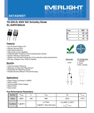
1. Ürün Genel Bakış
EL-SAF01 665JA, yüksek verimlilik ve yüksek frekanslı güç dönüştürme uygulamaları için özel olarak tasarlanmış bir silisyum karbür Schottky bariyer diyottur. Standart TO-220-2L paketini kullanan bu cihaz, silisyum karbürün üstün malzeme özelliklerinden yararlanarak geleneksel silisyum tabanlı diyotları çok aşan bir performans sergiler. Temel işlevi tek yönlü akım iletimi sağlamak olup, aynı zamanda son derece düşük anahtarlama kayıpları ve ters kurtarma yüküne sahiptir. Bu özellikleri, onu verimlilik ve güç yoğunluğu açısından zorlu gereksinimleri olan modern güç kaynakları ve invertörler için ideal bir seçim haline getirir.
Bu bileşenin ana hedef pazarı, anahtarlamalı güç kaynakları, güneş enerjisi dönüştürme sistemleri, kesintisiz güç kaynakları, motor sürücü kontrolörleri ve veri merkezi güç altyapısı üzerinde çalışan tasarımcılar ve mühendislerdir. Temel avantajı, daha yüksek frekanslı sistem tasarımlarını destekleyerek, pasif bileşenlerin (indüktörler ve kapasitörler gibi) boyutlarının küçültülmesini ve böylece sistemin genel maliyet ve hacminde tasarruf sağlanmasını mümkün kılmasıdır. Ayrıca, düşük termal direnç özelliği, soğutma gereksinimlerini azaltarak daha basit ve daha güvenilir bir ısı yönetimi çözümünün uygulanmasına yardımcı olur.
2. Derinlemesine Teknik Parametre Analizi
2.1 Elektriksel Özellikler
Elektriksel parametreler, diyotun belirli koşullar altındaki çalışma sınırlarını ve performansını tanımlar.
- Maksimum tekrarlayan tepe ters gerilimi:650V. Bu, diyotun ters öngerilim yönünde delinme olmadan dayanabileceği maksimum anlık gerilimdir. 400V AC doğrultma veya yükseltici PFC kademesi gibi uygulamalar için gerilim değerini tanımlar.
- Sürekli İleri Akım:16A. Bu, cihazın sürekli olarak iletebileceği maksimum ortalama ileri akımdır, genellikle kasa sıcaklığı 25°C iken belirtilir. Daha yüksek ortam sıcaklıklarında güç düşürme gerekir.
- İleri Voltaj:IF=16A, Tj=25°C'de tipik değer 1.5V, maksimum değer 1.85V'dir. Bu parametre, iletim kayıplarının hesaplanması için çok önemlidir. Veri sayfası ayrıca maksimum eklem sıcaklığındaki VF değerini belirtir; bu değer genellikle daha yüksektir ve en kötü durum kayıp hesaplamaları için çok önemlidir.
- Ters Akım:Çok düşük sızıntı akımı, VR=520V, Tj=25°C'de tipik değer 2µA'dır. Yüksek sıcaklıklarda bile sızıntı akımı yönetilebilir seviyelerde kalır. Düşük sızıntı akımı bekleme güç tüketimini en aza indirir.
- Toplam Kapasitans Yükü:Bu, SiC Schottky diyotlarının kilit bir parametresidir ve VR=400V'de tipik değeri 22nC'dir. Geleneksel diyotların aksine, SiC Schottky diyotlarında azınlık taşıyıcı depolaması yoktur, bu nedenle anahtarlama kayıpları büyük ölçüde kapasitiftir. QC, her anahtarlama döngüsünde sağlanması/serbest bırakılması gereken yükü temsil eder ve doğrudan anahtarlama kayıplarını etkiler. Bu düşük değer, yüksek frekanslı çalışmayı mümkün kılar.
2.2 Termal Özellikler
Termal yönetim, güvenilirlik ve performans için kritik öneme sahiptir.
- Bağlantı noktasından kılıfa ısıl direnç:Tipik değer 1.3°C/W'dir. Bu düşük değer, yarı iletken bağlantı noktasından paket kılıfına ısı transferinin verimli olduğunu gösterir. Güç tüketiminden kaynaklanan ısının, kılıfa bağlı bir soğutucu aracılığıyla etkili bir şekilde uzaklaştırılmasına olanak tanır.
- Maksimum bağlantı noktası sıcaklığı:175°C. Bu, silisyum karbür kavşağının ulaşabileceği mutlak maksimum sıcaklıktır. Bu sınıra yakın çalıştırmak uzun vadeli güvenilirliği azaltır, bu nedenle tasarımda bir pay bırakılması önerilir.
- Toplam Güç Tüketimi:Tc=25°C'de 115W. Bu, ideal soğutma koşullarında cihazın dağıtabileceği maksimum güçtür. Pratik uygulamalarda izin verilen dağıtım gücü daha düşüktür ve soğutucunun kasanın sıcaklığını düşük tutma yeteneğine bağlıdır.
2.3 Maksimum Değerler ve Sağlamlık
Bu değerler, kalıcı hasarın meydana gelebileceği mutlak sınırları tanımlar.
- Dalgalanma (Tekrarlanmayan) İleri Akım:10 ms yarım sinüs dalgası için 56A'dır. Bu değer, diyodun kısa devre veya darbe akımı olaylarına dayanma kapasitesini gösterir ve arıza koşullarında güvenilirliğin önemli bir faktörüdür.
- Depolama Sıcaklık Aralığı:-55°C ila +175°C. Cihazın enerji verilmediği durumlarda güvenli bir şekilde saklanabileceği sıcaklık aralığını tanımlar.
- Montaj Torku:M3 veya 6-32 vida için 0.8 ila 8.8 N·m'dir. Uygun tork, paket ısı emici ile soğutucu arasında iyi bir termal temas için çok önemlidir.
3. Performans Eğrisi Analizi
Veri sayfası, detaylı tasarım için kritik öneme sahip olan cihaz davranışının çeşitli grafiksel temsillerini sağlar.
- İleri Yönlü Gerilim - İleri Yönlü Akım Karakteristiği:Bu grafik, farklı jonksiyon sıcaklıklarında ileri yönlü gerilim ile ileri yönlü akım arasındaki ilişkiyi gösterir. Sadece tabloda verilen tek bir veri noktası değil, çeşitli çalışma noktalarındaki iletim kayıplarının hassas hesaplanması için kullanılır. Eğri tipik olarak, belirli bir akım için VF'nin sıcaklık arttıkça hafifçe düştüğünü gösterir; bu bir Schottky diyotunun karakteristiğidir.
- Ters Gerilim - Ters Akım Karakteristiği:Ters kaçak akımın ters gerilimle ilişkisi, genellikle birden fazla sıcaklıkta çizilir. Bu, tasarımcıların kapalı durum kayıplarını anlamasına ve uygulamanın maksimum gerilim ve sıcaklığındaki kaçak akımın kabul edilebilir olduğundan emin olmasına yardımcı olur.
- Ters Gerilim - Eklem Kapasitansı Karakteristiği:Diyot bağlantı kapasitansının ters gerilimle nasıl değiştiğini gösterir. Kapasitans, ters gerilim arttıkça azalır. Bu grafik, kapasitif anahtarlama davranışını modellemek ve belirli bir çalışma gerilimindeki QC'yi hesaplamak için kritik öneme sahiptir.
- Maksimum İleri Akım - Kasa Sıcaklığı Karakteristiği:Maksimum izin verilen sürekli ileri akımın, kasa sıcaklığı yükseldikçe nasıl düşürülmesi gerektiğini gösterir. Bu, gerekli soğutucu performansını belirleyen termal tasarımın ana grafiğidir.
- Güç Tüketimi - Kasa Sıcaklığı İlişkisi:Akım düşürme işlemine benzer şekilde, bu, maksimum izin verilen güç tüketiminin kasa sıcaklığı arttıkça nasıl azaldığını gösterir.
- Dalga Akımı - Darbe Genişliği Karakteristiği:Standart 10ms dışındaki darbe genişliklerindeki dalga akımı kapasitesini detaylandırır. Çeşitli geçici durumlar altındaki dayanıklılığın değerlendirilmesine olanak tanır.
- Depolama Kapasitörü Enerjisi - Ters Gerilim Karakteristiği:Depolanan kapasitör enerjisinin ters gerilimle ilişkisi çizilmiştir. Anahtarlama kaybı enerjisi bundan türetilebilir.
- Geçici Termal Empedans - Darbe Genişliği İlişkisi:Kısa güç darbeleri sırasındaki sıcaklık artışını değerlendirmek için kritik öneme sahiptir. Tek bir kısa darbe için termal empedans, kararlı durum bağlantı noktasından kılıfa ısıl dirençten daha düşüktür, bu da eklemi aşırı ısınmadan daha yüksek anlık güce izin verir.
4. Mekanik ve Paketleme Bilgileri
4.1 Paket Şekli ve Boyutları
Bu cihaz, endüstri standardı TO-220-2L kılıfı kullanır. Veri sayfasındaki kritik boyutlar şunları içerir:
- Toplam uzunluk: 15.6 mm
- 总宽度:9.99 mm总高度:4.5 mm
- Bacak Aralığı: 5.08 mm
- Montaj Deliği Mesafesi: 8.70 mm
- Isı emici boyutları ve mekanik entegrasyon ile PCB ped tasarımını kolaylaştırmak için pin şekillendirme detayları sağlanmıştır.
4.2 Bacak Yapılandırması ve Polarite
Pin tanımları açıktır:
- Pin 1:Katot.
- Pin 2:Anot.
- Kasa:Bu metal soğutucu, elektriksel olarak katot ile bağlantılıdır. Bu bağlantı, güvenlik ve tasarım açısından kritiktir: soğutucu katot potansiyelinde olacaktır, bu nedenle devrenin diğer kısımları farklı bir potansiyeldeyse yalıtılması gerekir. Uygun bir yalıtım kiti kullanılmalıdır.
4.3 Önerilen PCB Lehim Padi Yerleşimi
PCB tasarımı için, yüzey montajlı bir bacak şekilli lehim pedi yerleşimi önerilmiştir. Bu, bileşen PCB'ye monte edildiğinde iyi oluşmuş ve mekanik olarak sağlam bir lehim bağlantısı sağlar ve genellikle bir ısı emici ile birlikte kullanılır.
5. Kaynak ve Montaj Kılavuzu
Sağlanan alıntılarda ayrıntılı bir yeniden akış lehimleme eğrisi bulunmamasına rağmen, TO-220 paketli güç cihazları için genel kılavuz aşağıdaki gibidir:
- İşlem:Statik elektrik deşarjına karşı koruma önlemlerine dikkat edin, çünkü silisyum karbür cihazlar daha hassas olabilir.
- Lehimleme:Bacakların delikli montajı için standart dalga lehimleme veya elle lehimleme teknikleri kullanılabilir. Paket gövde sıcaklığı, maksimum depolama sıcaklığını uzun süre aşmamalıdır. Yüzey montaj bacak şekillendirmesi için kurşunsuz bileşenlerin standart reflow lehimleme eğrisine uyun.
- Soğutucu montajı:
- Radyatör ve diyot soğutucu plakasının montaj yüzeyinin temiz, düz ve çapaksız olduğundan emin olun.
- Isı transferini iyileştirmek için ince ve düzgün bir ısı ara yüz malzemesi tabakası uygulayın.
- Elektriksel yalıtım gerekiyorsa, yalıtkan mesafe pulu ve omuzlu pul kullanılan vidaları tercih edin. Yalıtkanın her iki tarafına termal macun uygulayın.
- Diyotu sabitlemek için belirtilen montaj torkuyla, M3 veya 6-32 vida ve somun kullanın. Paketi hasar almaktan veya vida ağızlarının bozulmasından kaçınmak için aşırı sıkmaktan sakının.
- Depolama:Belirtilen sıcaklık aralığında, kuru ve statik elektrikten korunmuş bir ortamda saklayınız.
6. Uygulama Önerileri
6.1 Tipik Uygulama Devresi
- Güç Faktörü Düzeltme Yükseltici Diyotu:Sürekli İletim Modu yükseltici PFC devrelerinde, diyotun düşük QC'si ve hızlı anahtarlama özelliği, yüksek anahtarlama frekanslarında yüksek verimlilik elde etmek için çok önemlidir. Ana anahtar iletimdeyken yüksek voltaj stresine maruz kalır.
- Solar Mikro İnvertör Çıkış Katı:Yüksek frekanslı inverter köprüsünde veya serbest döngü diyotu olarak kullanılır. Yüksek sıcaklık kapasitesi, güneş enerjisi uygulamalarının zorlu çevre koşullarına uygundur.
- Kesintisiz Güç Kaynağı İnvertörü/Konvertörü:DC-AC inverter veya DC-DC konvertör katında serbest döngü veya kenetleme diyotu olarak kullanılarak genel sistem verimliliğini artırır.
- Motor Sürücü DC Bara Kelepçeleme/Serbest Dolaşım Diyotu:Motor sargılarından gelen endüktif enerjiyi kelepçeleyerek, IGBT veya MOSFET'i voltaj sivrilerinden korur.
6.2 Kritik Tasarım Hususları
- Tampon Devresi:Anahtarlama hızının çok yüksek ve QC'nin düşük olması nedeniyle, devredeki parazitik endüktans önemli bir aşırı gerilime yol açar. Döngü alanını en aza indirmek için PCB düzeninin dikkatlice tasarlanması çok önemlidir. Halkalamayı bastırmak için diyot üzerinde bir RC tampon devresi kullanmak gerekebilir.
- Termal Tasarım:Toplam güç kaybını hesaplayın. Maksimum jonksiyon sıcaklığı, jonksiyondan kılıfa ısıl direnç ve tahmini soğutucu ısıl direnci kullanarak jonksiyon sıcaklığının güvenlik marjı içinde kalmasını sağlayın.
- Paralel Çalıştırma:Veri sayfası, cihazın termal kaçak olmadan paralel kullanılabileceğini belirtmektedir. Bu, yüksek akımlarda ileri voltajın pozitif sıcaklık katsayısına sahip olmasından kaynaklanır, bu da akım paylaşımını teşvik eder. Ancak, en iyi akım paylaşımı için düzenin simetrik olduğundan emin olunmalı ve ilgili anahtarlar sürülürken bağımsız gate dirençleri kullanılmalıdır.
- Voltaj Derecelendirmesi:Uzun vadeli güvenilirliği artırmak için, özellikle yüksek sıcaklık veya yüksek güvenilirlik gerektiren uygulamalarda, çalışma ters geriliminin düşürülmesi dikkate alınmalıdır.
7. Teknik Karşılaştırma ve Avantajlar
Standart silikon hızlı kurtarma diyotları ve hatta ultra hızlı kurtarma diyotları ile karşılaştırıldığında, EL-SAF01 665JA belirgin avantajlara sahiptir:
- Esasen sıfır ters kurtarma yükü:Silikon diyotlar, azınlık taşıyıcı depolaması nedeniyle önemli bir Qrr'ye sahiptir, bu da kapanma sırasında büyük akım sivri değerlerine ve kayıplara yol açar. Silisyum karbür Schottky diyotları çoğunluk taşıyıcı cihazlardır, bu nedenle Qrr ihmal edilebilir düzeydedir. Anahtarlama kayıpları tamamen kapasitiftir ve Qrr tabanlı kayıplardan çok daha düşüktür.
- Daha yüksek çalışma sıcaklığı:Silisyum karbürün geniş bant aralığı, maksimum jonksiyon sıcaklığının 175°C'ye ulaşmasına izin verirken, birçok silikon diyot için bu değer 150°C veya 125°C'dir. Bu, daha sıcak ortamlarda çalışabilmesini veya daha küçük soğutucuların kullanılmasını sağlar.
- Daha Yüksek Anahtarlama Frekansı Kabiliyeti:Düşük QC ve sıfır Qrr kombinasyonu, 100 kHz'in çok üzerindeki frekanslarda verimli çalışmayı mümkün kılarak manyetik bileşenlerin önemli ölçüde küçültülmesine olanak tanır.
- Daha düşük ileri voltaj yüksek sıcaklıklarda:Oda sıcaklığındaki VF değeri silikon Schottky diyotlarla karşılaştırılabilir olsa da, silisyum karbür (SiC) Schottky diyotların VF değeri sıcaklık arttıkça daha az yükselir, bu da daha iyi yüksek sıcaklık iletim performansı sağlar.
8. Sıkça Sorulan Sorular
8.1 Teknik Parametrelere Dayalı
S: QC 22nC'dir. Anahtarlama kayıpları nasıl hesaplanır?
C: Her anahtarlama döngüsündeki enerji kaybı yaklaşık olarak E_sw ≈ 0.5 * QC * V'dir; burada V, kapanma sırasındaki ters gerilimdir. Örneğin, 400V'de E_sw ≈ 0.5 * 22nC * 400V = 4.4µJ'dür. Anahtarlama frekansı ile çarpılarak güç kaybı elde edilir: P_sw = E_sw * f_sw. 100 kHz'de P_sw ≈ 0.44W'dır.
Soru: Neden gövde katoda bağlanır? Her zaman izolasyon gerekli midir?
Cevap: Termal ve mekanik nedenlerle, iç çip elektriksel olarak katot soğutucuya bağlı bir alt tabaka üzerine monte edilmiştir. Eğer soğutucu devredeki katot potansiyelinden farklıysa, izolasyon gereklidir. Eğer katot topraklanmışsa ve soğutucu da topraklanmışsa, izolasyon gerekli olmayabilir, ancak genellikle güvenlik için en iyi uygulama olarak kullanılır.
Soru: Bu diyotu mevcut bir devrede doğrudan bir silikon diyotla değiştirebilir miyim?
Cevap: Doğrudan değiştirme yapılamaz. Gerilim ve akım değerleri uyumlu olsa da, son derece hızlı anahtarlama hızı, devre parazitik parametreleri nedeniyle ciddi gerilim aşımına ve elektromanyetik girişime yol açabilir; bu sorunlar daha yavaş silikon diyotlar için geçerli değildir. PCB yerleşimi ve snubber devre tasarımı yeniden değerlendirilmelidir.
9. Pratik Tasarım ve Uygulama Örnekleri
Vaka Çalışması: Yüksek Yoğunluklu 2kW Sunucu Güç Kaynağı PFC Aşaması.Bir tasarımcı, 80kHz CCM yükseltici PFC'de 600V/15A'lık bir silikon ultra hızlı diyotu EL-SAF01 ile değiştirdi. Hesaplamalar, silisyum karbür diyotun anahtarlama kayıplarını yaklaşık %60 azalttığını ve iletim kayıplarını hafifçe iyileştirdiğini gösterdi. Diyot başına 0.86W'lık tasarruf edilen kayıp, anahtarlama frekansının 140kHz'e yükseltilmesine izin verdi, bu da yükseltici endüktör boyutunu yaklaşık %40 küçülterek güç yoğunluğunu artırma hedefine ulaşılmasını sağladı. Toplam kayıpların azalması nedeniyle mevcut soğutucu yeterli kalmaya devam etti.
Vaka Çalışması: Solar Mikro İnvertör H Köprüsü.300W'lık bir mikro invertörde, dört adet EL-SAF01 diyotu, H köprüsü MOSFET'lerinin serbest dönüş diyotları olarak kullanıldı. Yüksek sıcaklık derecelendirmesi, çatı ortamında muhafaza sıcaklığının 70°C'yi aşabileceği durumlarda güvenilirliği sağladı. Düşük QC, yüksek anahtarlama frekanslarında kayıpları en aza indirerek, güneş enerjisi toplama için kritik olan daha yüksek genel dönüşüm verimliliğine katkıda bulundu.
10. Çalışma Prensibi
Schottky diyotları, standart PN birleşim diyotlarından farklı olarak metal-yarı iletken birleşiminden oluşur. EL-SAF01, yarı iletken olarak silisyum karbür kullanır. Metal-SiC arayüzünde oluşan Schottky bariyeri yalnızca çoğunluk taşıyıcıların iletimine izin verir. İleri yönde polarma uygulandığında, elektronlar yarı iletkenden metale enjekte olur ve göreceli olarak düşük bir ileri voltaj düşüşü ile akım akışına izin verir. Ters yönde polarma uygulandığında ise Schottky bariyeri akım akışını engeller. PN diyotlarından temel farkı, azınlık taşıyıcı enjeksiyonu ve depolanmasının olmamasıdır. Bu, sürüklenme bölgesinde depolanan yük ile ilişkili bir difüzyon kapasitansı olmadığı anlamına gelir ve bu da "sıfır ters kurtarma" özelliğini ortaya çıkarır. Tek kapasitans, voltaja bağlı olan ve ölçülebilir bir QC (yük kapasitansı) üreten eklem tükenme tabakası kapasitansıdır. Silisyum karbürün geniş bant aralığı, yüksek delinme alan şiddeti sağlar ve bu da nispeten küçük bir çip boyutunda 650V derecelendirmesinin mümkün olmasını sağlar. Ayrıca yüksek termal iletkenliği ısı dağılımına yardımcı olur.
11. Teknoloji Trendleri
Silisyum karbür güç cihazları, Schottky diyotlar ve MOSFET'ler dahil olmak üzere, güç elektroniğinde daha yüksek verimlilik, frekans ve güç yoğunluğuna doğru önemli bir eğilimi temsil eder. Piyasa, 600-650V cihazlardan daha yüksek voltaj seviyelerine geçiş yapmaktadır. Aynı zamanda, wafer boyutlarının büyümesi ve üretim verimliliğinin artmasıyla birlikte amper başına maliyetin düşmesi bir başka eğilimdir. Entegrasyon da bir diğer eğilimdir; silisyum karbür MOSFET ve Schottky diyotları birleştiren modüller ortaya çıkmıştır. Ayrıca, ileri yönlü voltaj düşüşünü daha da azaltmak ve güvenilirliği artırmak için Schottky bariyer arayüzünü iyileştirmeye yönelik araştırmalar devam etmektedir. Küresel olarak, enerji verimliliği standartları ile ulaşım ve yenilenebilir enerji sistemlerinin elektrifikasyonu, silisyum karbürün benimsenmesini teşvik etmektedir.
LED Özellik Terimlerinin Ayrıntılı Açıklaması
LED Teknik Terimlerinin Tam Açıklaması
I. Optoelektronik Performans Temel Göstergeleri
| Terimler | Birim/Gösterim | Basit Açıklama | Neden Önemli |
|---|---|---|---|
| Işık Etkinliği (Luminous Efficacy) | lm/W (lümen/vat) | Watt başına üretilen ışık akısı, ne kadar yüksekse o kadar enerji tasarruflu demektir. | Aydınlatma armatürünün enerji verimliliği sınıfını ve elektrik maliyetini doğrudan belirler. |
| Işık Akısı (Luminous Flux) | lm (lümen) | Bir ışık kaynağının yaydığı toplam ışık miktarı, halk arasında "parlaklık" olarak adlandırılır. | Lambanın yeterince parlak olup olmadığına karar verin. |
| Işık Açısı (Viewing Angle) | ° (derece), örneğin 120° | Işık şiddetinin yarıya düştüğü açı, ışık hüzmesinin genişliğini veya darlığını belirler. | Aydınlatma alanını ve düzgünlüğünü etkiler. |
| Renk Sıcaklığı (CCT) | K (Kelvin), örn. 2700K/6500K | Işığın renk sıcaklığı; düşük değerler sarı/sıcak, yüksek değerler beyaz/soğuk tonlara kayar. | Aydınlatma atmosferini ve uygun kullanım senaryolarını belirler. |
| Renksel Geriverim İndeksi (CRI / Ra) | Birim yok, 0–100 | Işık kaynağının nesnelerin gerçek renklerini yansıtma yeteneği, Ra≥80 tercih edilir. | Renk gerçekliğini etkiler; alışveriş merkezleri, sanat galerileri gibi yüksek gereksinimli mekanlarda kullanılır. |
| Renk toleransı (SDCM) | MacAdam elips adım sayısı, örn. "5-step" | Renk tutarlılığının nicel göstergesi, adım sayısı ne kadar küçükse renk o kadar tutarlıdır. | Aynı parti aydınlatma armatürlerinin renginde fark olmamasını garanti eder. |
| Dominant Wavelength | nm (nanometre), örneğin 620nm (kırmızı) | Renkli LED'lerin renklerine karşılık gelen dalga boyu değerleri. | Kırmızı, sarı, yeşil gibi tek renkli LED'lerin renk tonunu belirler. |
| Spektral Dağılım (Spectral Distribution) | Dalga boyu vs. Yoğunluk eğrisi | LED'in yaydığı ışığın farklı dalga boylarındaki yoğunluk dağılımını gösterir. | Renksel geriverim ve renk kalitesini etkiler. |
İki, Elektriksel Parametreler
| Terimler | Semboller | Basit Açıklama | Tasarım Hususları |
|---|---|---|---|
| İleri Yönlü Gerilim (Forward Voltage) | Vf | LED'in yanması için gereken minimum voltaj, "başlangıç eşiği" gibidir. | Sürücü güç kaynağı voltajı ≥Vf olmalıdır, birden fazla LED seri bağlandığında voltajlar toplanır. |
| Forward Current | Eğer | LED'in normal şekilde ışık yaymasını sağlayan akım değeri. | Genellikle sabit akım sürücüsü kullanılır, akım parlaklığı ve ömrü belirler. |
| Maksimum Darbe Akımı (Pulse Current) | Ifp | Kısa süreli olarak tolere edilebilen tepe akımı, ışık ayarlama veya flaş için kullanılır. | Darbe genişliği ve görev döngüsü sıkı bir şekilde kontrol edilmelidir, aksi takdirde aşırı ısınma ve hasar meydana gelir. |
| Ters Gerilim (Reverse Voltage) | Vr | LED'in dayanabileceği maksimum ters gerilim, aşılırsa delinme meydana gelebilir. | Devrede ters bağlantı veya voltaj darbelerinin önlenmesi gerekir. |
| Thermal Resistance | Rth (°C/W) | Isığın çipten lehim noktasına iletilmesindeki direnç, değer ne kadar düşükse ısı dağılımı o kadar iyidir. | Yüksek termal direnç, daha güçlü bir soğutma tasarımı gerektirir, aksi takdirde bağlantı sıcaklığı yükselir. |
| Elektrostatik deşarj dayanımı (ESD Immunity) | V (HBM), örneğin 1000V | Statik şok direnci, değer ne kadar yüksekse statik elektrikten o kadar az zarar görür. | Üretimde, özellikle yüksek hassasiyetli LED'ler için statik elektrik önlemleri alınmalıdır. |
III. Isı Yönetimi ve Güvenilirlik
| Terimler | Kritik Göstergeler | Basit Açıklama | Etki |
|---|---|---|---|
| Kavşak Sıcaklığı (Junction Temperature) | Tj (°C) | LED çipinin içindeki gerçek çalışma sıcaklığı. | Her 10°C düşüşte, ömür iki katına çıkabilir; aşırı yüksek sıcaklık ışık azalmasına ve renk kaymasına neden olur. |
| Işık Azalması (Lumen Depreciation) | L70 / L80 (saat) | Parlaklığın başlangıç değerinin %70'ine veya %80'ine düşmesi için gereken süre. | LED'in "kullanım ömrü"nü doğrudan tanımlar. |
| Lümen Bakım Oranı (Lumen Maintenance) | % (örneğin %70) | Belirli bir süre kullanımdan sonra kalan parlaklığın yüzdesi. | Uzun süreli kullanım sonrası parlaklık koruma yeteneğini karakterize eder. |
| Color Shift | Δu′v′ veya MacAdam Elipsi | Kullanım sürecindeki renk değişim derecesi. | Aydınlatma sahnesinin renk tutarlılığını etkiler. |
| Thermal Aging | Malzeme performansında düşüş | Uzun süreli yüksek sıcaklığa bağlı olarak paketleme malzemesinde bozulma. | Parlaklıkta azalma, renk değişimi veya açık devre arızasına yol açabilir. |
IV. Paketleme ve Malzemeler
| Terimler | Yaygın Türler | Basit Açıklama | Özellikler ve Uygulamalar |
|---|---|---|---|
| Paketleme Türü | EMC, PPA, Seramik | Çipi koruyan ve optik, termal arayüz sağlayan kasa malzemesi. | EMC iyi ısı direncine ve düşük maliyete sahiptir; seramik üstün ısı dağıtımı ve uzun ömür sunar. |
| Çip yapısı | Düz Yüzeyli, Ters Çevrilmiş (Flip Chip) | Çip Elektrot Düzenleme Yöntemi. | Ters çevirme daha iyi ısı dağılımı ve daha yüksek ışık verimliliği sağlar, yüksek güç için uygundur. |
| Fosfor kaplama | YAG, silikat, nitrür | Mavi ışık çipi üzerine kaplanır, kısmen sarı/kırmızı ışığa dönüştürülür ve beyaz ışık oluşturmak için karıştırılır. | Farklı fosforlar, ışık verimliliğini, renk sıcaklığını ve renksel geriverimi etkiler. |
| Lens/Optik Tasarımı | Düzlem, Mikrolens, Tam Yansıma | Paketleme yüzeyindeki optik yapı, ışık dağılımını kontrol eder. | Işık açısını ve ışık dağılım eğrisini belirler. |
V. Kalite Kontrolü ve Sınıflandırma
| Terimler | Dosya İçeriği | Basit Açıklama | Amaç |
|---|---|---|---|
| Işık Akısı Sınıflandırması | Kodlar örneğin 2G, 2H | Parlaklık seviyelerine göre gruplandırılır, her grubun minimum/maksimum lümen değeri vardır. | Aynı parti ürünlerin parlaklığının tutarlı olmasını sağlayın. |
| Voltaj sınıflandırması | Kodlar örneğin 6W, 6X | İleri yönlü voltaj aralığına göre gruplandırın. | Sürücü güç kaynağı eşleştirmesini kolaylaştırmak ve sistem verimliliğini artırmak için. |
| Renk Ayırımı Sınıflandırması | 5-adımlı MacAdam elipsi | Renk koordinatlarına göre gruplandırın, renklerin çok dar bir aralıkta kalmasını sağlayın. | Renk tutarlılığını sağlayın, aynı armatür içinde renk düzensizliğinden kaçının. |
| Renk sıcaklığı sınıflandırması | 2700K, 3000K vb. | Renk sıcaklığına göre gruplandırılmıştır, her grubun karşılık gelen koordinat aralığı vardır. | Farklı senaryoların renk sıcaklığı ihtiyaçlarını karşılar. |
VI. Test ve Sertifikasyon
| Terimler | Standart/Test | Basit Açıklama | Anlam |
|---|---|---|---|
| LM-80 | Lümen Bakım Testi | Sabit sıcaklık koşullarında uzun süreli yakma, parlaklık azalma verilerini kaydetme. | LED ömrünü tahmin etmek için kullanılır (TM-21 ile birlikte). |
| TM-21 | Ömür Tahmin Standardı | LM-80 verilerine dayalı olarak gerçek kullanım koşullarında ömür tahmini. | Bilimsel ömür tahmini sağlar. |
| IESNA standardı | Aydınlatma Mühendisliği Derneği Standardı | Optik, elektrik ve termal test yöntemlerini kapsar. | Sektörde kabul görmüş test temeli. |
| RoHS / REACH | Çevre Sertifikası | Ürünün zararlı maddeler (kurşun, cıva gibi) içermediğinden emin olun. | Uluslararası pazara giriş koşulları. |
| ENERGY STAR / DLC | Enerji Verimliliği Sertifikası | Aydınlatma ürünleri için enerji verimliliği ve performans sertifikasyonu. | Genellikle devlet alımları ve sübvansiyon projelerinde kullanılır, piyasa rekabet gücünü artırır. |