目录
1. 产品概述
ELM456系列是专为电力电子高可靠性隔离而设计的一类智能功率模块光耦。这些器件将红外发光二极管与高增益光探测器通过光学耦合集成在一个紧凑的、行业标准的5引脚小外形封装内。其主要功能是在低压控制电路和高压功率级(如电机驱动器和逆变器中常见的)之间提供稳健的电气隔离和信号传输。
该系列的核心优势在于其高达3750 Vrms的高隔离能力,这对于高压应用中的安全性和抗噪性至关重要。器件专为表面贴装设计,便于自动化组装工艺,并有助于实现紧凑的PCB设计。符合无卤素、无铅、RoHS和REACH标准,突显了其适用于现代环保型电子制造的适用性。
2. 技术规格与深度解读
2.1 绝对最大额定值
绝对最大额定值定义了可能导致器件永久损坏的应力极限。关键参数包括输入LED的正向电流为20 mA,输出电源电压为30 V,以及输出电流为15 mA。在受控湿度条件下,隔离电压额定值为3750 Vrms(持续一分钟)。工作温度范围为-40°C至+85°C,表明其在工业环境下的稳健性能。260°C下10秒的焊接温度额定值与标准的无铅回流焊曲线一致。F2.2 电气特性CC电气特性分为输入、输出和传输参数,提供了典型工作条件下的全面性能概况。O2.2.1 输入特性ISO输入LED的正向电压在正向电流为10 mA时典型值为1.45V,最大值为1.8V。这种低正向电压有助于降低驱动电路的功耗。在5V反向偏压下,反向电流最大为10 µA,表明具有良好的二极管特性。输入电容典型值为60 pF,这是在高速开关应用中需要考虑的一个因素,以避免对驱动器造成过大的负载。
2.2.2 输出与传输特性
电源电流消耗较低,当输入关闭时,高电平电源电流典型值为0.7 mA。电流传输比在特定条件下规定为最小220%。高CTR确保相对较小的输入电流能有效驱动输出级,提高效率。在指定条件下,低电平输出电压典型值为0.15V,确保稳固的逻辑低电平状态。
2.3 开关特性
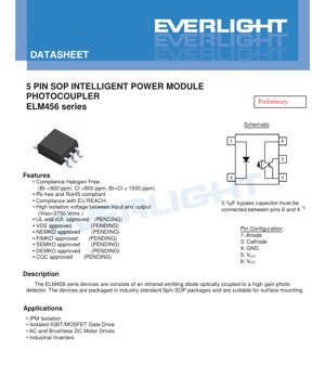
开关性能对于PWM栅极驱动等时序敏感应用至关重要。输出高电平传播延迟时间典型值为150 ns,而输出低电平延迟典型值为450 ns。脉冲宽度失真典型值为300 ns。这些不对称延迟必须在系统时序设计中加以考虑,以防止信号失真。共模瞬态抗扰度是关键鲁棒性指标,规定逻辑高电平和逻辑低电平状态下的最小值均为10 kV/µs。这种高CMTI额定值确保了在具有快速变化共模电压的嘈杂环境中的可靠运行。F3. 性能曲线分析F数据手册引用了典型的光电特性曲线。虽然提供的文本中没有详细说明具体图表,但此类曲线通常说明了正向电流与正向电压之间的关系、CTR的温度依赖性以及传播延迟随负载或温度的变化。分析这些曲线对于设计人员理解器件在非标准条件下的行为、优化效率和速度的工作点以及确保在预期温度范围内的可靠性能至关重要。F4. 机械与封装信息R4.1 引脚配置与功能IN器件采用5引脚SOP配置。引脚排列如下:引脚1:阳极,引脚3:阴极;引脚4:地,引脚5:电源电压,引脚6:输出。一个关键的设计说明指出,必须在引脚6和引脚4之间连接一个0.1 µF的旁路电容,以确保稳定运行并最小化噪声。
4.2 封装尺寸与推荐焊盘布局
数据手册包含SOP封装的详细封装尺寸图。它还提供了表面贴装的推荐焊盘布局。遵循此推荐的焊盘布局对于实现可靠的焊点、适当的机械稳定性和回流焊过程中的有效散热至关重要。焊盘设计考虑了焊料圆角形成和防止立碑等因素。CCH5. 焊接与组装指南F文档提供了具体的焊接注意事项,详细说明了符合IPC/JEDEC J-STD-020D无铅回流焊标准的最高壳体温度曲线。该曲线的关键参数包括:在60-120秒内从150°C预热至200°C,峰值温度为260°C,以及高于液相线的时间在60-100秒之间。器件最多可承受三次回流焊循环。遵循此曲线对于防止塑料封装和内部半导体芯片的热损伤、确保长期可靠性至关重要。CC6. 包装与订购信息F6.1 订购零件编号系统O零件编号遵循格式:ELM456(Y)-VG。"EL"前缀表示制造商。"M456"是基础器件编号。"Y"代表编带和卷盘选项。"V"表示VDE认证。"G"表示无卤素结构。TA和TB选项在卷盘的进料方向上有所不同,以适应不同的贴片机配置。两种选项每卷均包装1000个器件。CC6.2 编带与卷盘规格OL提供了详细的编带尺寸,包括口袋尺寸、孔直径、间距和编带宽度。这些尺寸对于正确设置自动化组装设备以确保正确的元件进料和放置至关重要。
6.3 器件标识
器件在顶面进行标识。标识包括:"EL"、"M456"、一位年份代码、两位周代码以及VDE选项的"V"。此标识允许追溯生产日期和变体。PHL7. 应用建议PLH7.1 典型应用场景PHLELM456系列专为以下应用设计:智能功率模块隔离、隔离式IGBT/MOSFET栅极驱动、交流和无刷直流电机驱动以及工业逆变器。PLH7.2 设计考量与注意事项M设计人员必须考虑几个关键因素:旁路电容必须尽可能靠近器件引脚放置;不对称的传播延迟会影响传输的脉冲宽度,可能需要补偿;外部限流电阻必须与输入LED串联;输出通常需要一个上拉或负载电阻;PCB布局必须在电路的初级侧和次级侧之间保持足够的爬电距离和电气间隙。M8. 技术对比与差异化
虽然源文档未提供与特定竞争对手部件的直接比较,但可以根据ELM456系列公布的规格进行评估。关键差异化因素可能包括其高达3750 Vrms的隔离额定值、高CMTI与紧凑SOP封装的结合、无卤素和全面的环保合规性,以及符合全球公认安全标准的设计意图。
9. 常见问题解答(基于技术参数)
Q1: 高隔离电压的目的是什么? A1: 此额定值确保安全运行并防止低压控制电路和高压功率电路之间的危险击穿。它是许多连接主电源设备的安全要求,并提供强大的抗噪能力。
Q2: 为什么传播延迟时间不同? A2: 这种不对称性是内部光电探测器和放大器设计固有的。关断过程通常比开启过程慢。在时序关键的应用中必须考虑这一点,以避免脉冲失真。
Q3: 如何选择输入限流电阻的值? A3: 使用欧姆定律计算。确保在最坏情况下正向电流不超过20 mA。保证CTR的典型正向电流为10 mA。OUTQ4: "共模瞬态抗扰度"是什么意思,为什么重要? A4: CMTI衡量器件抑制隔离屏障两侧出现的快速电压瞬变的能力。低CMTI可能导致输出错误地产生毛刺。10 kV/µs的额定值对于工业电机控制应用来说是良好的。CCQ5: 数据手册列出许多安全认证为"待定"。我可以在最终产品中使用此部件吗? A5: 对于需要认证安全批准的产品,必须在最终确定设计并投入生产之前,向制造商或分销商核实这些认证的最终状态。使用没有所需认证的器件可能会阻碍您的最终产品获得其自身的安全认证。CC10. 实际设计与使用案例
案例:三相BLDC电机逆变器的隔离栅极驱动器 在一个典型的三相逆变器中,使用六个ELM456器件。微控制器的PWM信号通过限流电阻馈入六个ELM456器件的阳极。每个光耦的输出驱动专用栅极驱动IC的输入。ELM456的3750 Vrms隔离保护敏感的微控制器免受高压直流母线的影响。高CMTI确保来自逆变器的嘈杂开关瞬变不会导致栅极信号的错误触发。紧凑的SOP封装允许所有六个隔离器整齐地放置在微控制器附近。设计必须包括直接放置在每个ELM456的电源/地引脚上的六个0.1 µF旁路电容。
11. 工作原理简介
光耦是一种利用光在两个隔离电路之间传输电信号的器件。ELM456在一个不透明的封装内包含两个主要部分。在输入侧,红外发光二极管将输入电信号转换为成比例的红外光强度。该光穿过透明的隔离屏障。在输出侧,光电探测器接收此光并将其转换回电信号。关键点在于屏障两侧没有电气连接,只有光学连接,从而提供了电气隔离。ELM456输出级中的高增益放大器使其能够实现高电流传输比,这意味着小的输入电流能产生更大的可用输出电流。
12. 技术发展趋势P电气隔离领域正在不断发展。虽然像ELM456这样的传统光耦因其成熟度、成本效益和高电压额定值而仍然非常流行,但替代技术正在获得关注。电容式隔离器使用穿过二氧化硅屏障的变化电场,提供更高的速度、更低的功耗和更高的集成度。磁性隔离器使用变压器线圈,也提供高速度和鲁棒性。然而,光耦在极高的隔离电压能力、简单性以及在恶劣环境中经过验证的长期可靠性方面仍然具有显著优势。光耦技术本身的趋势包括追求更高的速度、更高的CMTI、更低的功耗、更小的封装尺寸以及集成更多功能。正如ELM456所示,向无卤素和增强材料合规性的转变是由环境法规驱动的普遍行业趋势。
. Packaging and Ordering Information
.1 Ordering Part Number System
The part number follows the format: ELM456(Y)-VG. The "EL" prefix denotes the manufacturer. "M456" is the base device number. "Y" represents the tape and reel option (TA or TB). "V" indicates VDE approval (optional, noted as pending in this document). "G" signifies halogen-free construction. The TA and TB options differ in the feed direction from the reel, accommodating different pick-and-place machine configurations. Both options pack 1000 units per reel.
.2 Tape and Reel Specifications
Detailed tape dimensions are provided, including pocket size (A, B), hole diameters (Do, D1), pitch (P0, P1), and tape width (W). These dimensions are critical for setting up automated assembly equipment correctly to ensure proper component feeding and placement.
.3 Device Marking
Devices are marked on the top surface. The marking includes: "EL" (manufacturer code), "M456" (device number), a one-digit year code (Y), a two-digit week code (WW), and "V" for the VDE option. This marking allows for traceability of manufacturing date and variant.
. Application Suggestions
.1 Typical Application Scenarios
The ELM456 series is explicitly designed for:
- IPM (Intelligent Power Module) Isolation:Providing the necessary isolation between the microcontroller and the high-voltage IPM.
- Isolated IGBT/MOSFET Gate Drive:Driving the gates of power switches in half-bridge or full-bridge configurations while maintaining isolation.
- AC and Brushless DC Motor Drives:Isolating control signals in variable frequency drives and motor controllers.
- Industrial Inverters:Used in UPS systems, solar inverters, and other power conversion equipment.
.2 Design Considerations and Notes
Designers must consider several key factors:
- Bypass Capacitor:The mandatory 0.1 µF capacitor between VCCand GND (pins 6 & 4) must be placed as close as possible to the device pins to be effective.
- Propagation Delays:The asymmetric propagation delays (TPHLvs TPLH) will affect the transmitted pulse width. Compensation may be needed in software or via external circuitry if precise pulse integrity is required.
- Current Limiting Resistor:An external resistor is always required in series with the input LED (Anode, Pin 1) to limit the forward current (IF) to a safe value, typically between 5-16 mA as per application needs, and never exceeding 20 mA.
- Load Resistor:The output typically requires a pull-up or load resistor (RL) connected between VOUT(Pin 5) and VCC. The value of RLinfluences switching speed and current consumption; 350 Ω is used in the datasheet test conditions.
- Isolation Creepage and Clearance:PCB layout must maintain adequate creepage and clearance distances (as per relevant safety standards like IEC 60950-1 or IEC 61800-5-1) between the primary (input) and secondary (output) sides of the circuit, even though the device itself provides the isolation barrier.
. Technical Comparison and Differentiation
While a direct comparison with specific competitor parts is not provided in the source document, the ELM456 series can be evaluated based on its published specifications. Key differentiators likely include its high 3750 Vrms isolation rating, which may be superior to many standard photocouplers rated at 2500 Vrms or 5000 Vrms. The combination of high CMTI (10 kV/µs min) and a compact SOP package is advantageous for space-constrained, high-noise applications. The halogen-free and comprehensive environmental compliance (RoHS, REACH) is a significant advantage for markets with strict regulatory requirements. The pending approvals from major safety agencies (UL, cUL, VDE, etc.) indicate design intent for globally recognized safety standards.
. Frequently Asked Questions (Based on Technical Parameters)
Q1: What is the purpose of the high isolation voltage (3750 Vrms)?
A1: This rating ensures safe operation and prevents hazardous breakdown between the low-voltage control circuit and the high-voltage power circuit. It is a safety requirement for many mains-connected equipment (e.g., 230VAC/400VAC drives) and provides robust noise immunity.
Q2: Why are the propagation delay times (TPHLand TPLH) different?
A2: The asymmetry is inherent to the internal photodetector and amplifier design. The turn-off process (TPLH) is typically slower than turn-on (TPHL). This must be considered in timing-critical applications to avoid pulse distortion.
Q3: How do I select the value for the input current limiting resistor?
A3: Use Ohm's law: RLIMIT= (VDRIVE- VF) / IF. VDRIVEis your logic supply voltage (e.g., 3.3V, 5V). Use the typical VF(1.45V) for calculation, but ensure IFdoes not exceed 20 mA under worst-case conditions (min VDRIVE, min RLIMITtolerance). A typical IFfor guaranteed CTR is 10 mA.
Q4: What does "Common Mode Transient Immunity" mean, and why is it important?
A4: CMTI measures the device's ability to reject fast voltage transients that appear equally on both sides of the isolation barrier (e.g., due to switching noise in a motor drive). A low CMTI can cause the output to glitch falsely. A rating of 10 kV/µs is considered good for industrial motor control applications.
Q5: The datasheet lists many safety approvals as "PENDING." Can I use this part in a final product?
A5: For a product requiring certified safety approval (UL, VDE, etc.), you must verify the final status of these certifications with the manufacturer or distributor before finalizing the design and proceeding to production. Using a device without the required certification may prevent your end product from achieving its own safety certification.
. Practical Design and Usage Case
Case: Isolated Gate Driver for a 3-Phase BLDC Motor Inverter
In a typical 3-phase inverter driving a Brushless DC motor, six power switches (IGBTs or MOSFETs) are used. Each switch requires an isolated gate drive signal. The ELM456 can be used for each of these six channels. The microcontroller's PWM signals are fed into the anode (via current-limiting resistors) of six ELM456 devices. The output (VOUT) of each photocoupler drives the input of a dedicated gate driver IC, which then provides the high-current pulses needed to switch the IGBTs rapidly. The 3750 Vrms isolation of the ELM456 protects the sensitive microcontroller from the high-voltage DC bus (often 300-600VDC). The high CMTI ensures that the noisy switching transients from the inverter do not cause false triggering of the gate signals. The compact SOP package allows all six isolators to fit neatly near the microcontroller. The design must include six 0.1 µF bypass capacitors placed directly at the VCC/GND pins of each ELM456.
. Operating Principle Introduction
A photocoupler (or optocoupler) is a device that transfers electrical signals between two isolated circuits using light. The ELM456 consists of two main parts on separate die within a single, opaque package. On the input side, an infrared Light Emitting Diode (LED) converts the incoming electrical signal into a proportional intensity of infrared light. This light travels across a transparent isolation barrier (often a mold compound or air gap). On the output side, a photodetector (typically a phototransistor or a photo-diode plus amplifier) receives this light and converts it back into an electrical signal. The key is that there is no electrical connection—only an optical one—across the barrier, which provides the galvanic isolation. The high gain amplifier in the ELM456's output stage allows it to achieve a high Current Transfer Ratio (CTR), meaning a small input current produces a much larger usable output current.
. Technology Trends
The field of galvanic isolation is evolving. While traditional photocouplers like the ELM456 remain highly popular due to their maturity, cost-effectiveness, and high voltage ratings, alternative technologies are gaining traction. Capacitive isolators use changing electric fields across a silicon dioxide barrier, offering higher speed, lower power consumption, and higher integration (multiple channels in one package). Magnetic (inductive) isolators use transformer coils, also offering high speed and robustness. However, photocouplers continue to hold significant advantages in very high isolation voltage capabilities, simplicity, and proven long-term reliability in harsh environments. Trends within photocoupler technology itself include the push for higher speeds (lower propagation delays), higher CMTI for noisier applications, lower power consumption, smaller package footprints, and integration of more features like fail-safe outputs or I2C isolation. The move towards halogen-free and enhanced material compliance, as seen in the ELM456, is a universal industry trend driven by environmental regulations.
LED规格术语详解
LED技术术语完整解释
一、光电性能核心指标
| 术语 | 单位/表示 | 通俗解释 | 为什么重要 |
|---|---|---|---|
| 光效(Luminous Efficacy) | lm/W(流明/瓦) | 每瓦电能发出的光通量,越高越节能。 | 直接决定灯具的能效等级与电费成本。 |
| 光通量(Luminous Flux) | lm(流明) | 光源发出的总光量,俗称"亮度"。 | 决定灯具够不够亮。 |
| 发光角度(Viewing Angle) | °(度),如120° | 光强降至一半时的角度,决定光束宽窄。 | 影响光照范围与均匀度。 |
| 色温(CCT) | K(开尔文),如2700K/6500K | 光的颜色冷暖,低值偏黄/暖,高值偏白/冷。 | 决定照明氛围与适用场景。 |
| 显色指数(CRI / Ra) | 无单位,0–100 | 光源还原物体真实颜色的能力,Ra≥80为佳。 | 影响色彩真实性,用于商场、美术馆等高要求场所。 |
| 色容差(SDCM) | 麦克亚当椭圆步数,如"5-step" | 颜色一致性的量化指标,步数越小颜色越一致。 | 保证同一批灯具颜色无差异。 |
| 主波长(Dominant Wavelength) | nm(纳米),如620nm(红) | 彩色LED颜色对应的波长值。 | 决定红、黄、绿等单色LED的色相。 |
| 光谱分布(Spectral Distribution) | 波长 vs. 强度曲线 | 显示LED发出的光在各波长的强度分布。 | 影响显色性与颜色品质。 |
二、电气参数
| 术语 | 符号 | 通俗解释 | 设计注意事项 |
|---|---|---|---|
| 正向电压(Forward Voltage) | Vf | LED点亮所需的最小电压,类似"启动门槛"。 | 驱动电源电压需≥Vf,多个LED串联时电压累加。 |
| 正向电流(Forward Current) | If | 使LED正常发光的电流值。 | 常采用恒流驱动,电流决定亮度与寿命。 |
| 最大脉冲电流(Pulse Current) | Ifp | 短时间内可承受的峰值电流,用于调光或闪光。 | 脉冲宽度与占空比需严格控制,否则过热损坏。 |
| 反向电压(Reverse Voltage) | Vr | LED能承受的最大反向电压,超过则可能击穿。 | 电路中需防止反接或电压冲击。 |
| 热阻(Thermal Resistance) | Rth(°C/W) | 热量从芯片传到焊点的阻力,值越低散热越好。 | 高热阻需更强散热设计,否则结温升高。 |
| 静电放电耐受(ESD Immunity) | V(HBM),如1000V | 抗静电打击能力,值越高越不易被静电损坏。 | 生产中需做好防静电措施,尤其高灵敏度LED。 |
三、热管理与可靠性
| 术语 | 关键指标 | 通俗解释 | 影响 |
|---|---|---|---|
| 结温(Junction Temperature) | Tj(°C) | LED芯片内部的实际工作温度。 | 每降低10°C,寿命可能延长一倍;过高导致光衰、色漂移。 |
| 光衰(Lumen Depreciation) | L70 / L80(小时) | 亮度降至初始值70%或80%所需时间。 | 直接定义LED的"使用寿命"。 |
| 流明维持率(Lumen Maintenance) | %(如70%) | 使用一段时间后剩余亮度的百分比。 | 表征长期使用后的亮度保持能力。 |
| 色漂移(Color Shift) | Δu′v′ 或 麦克亚当椭圆 | 使用过程中颜色的变化程度。 | 影响照明场景的颜色一致性。 |
| 热老化(Thermal Aging) | 材料性能下降 | 因长期高温导致的封装材料劣化。 | 可能导致亮度下降、颜色变化或开路失效。 |
四、封装与材料
| 术语 | 常见类型 | 通俗解释 | 特点与应用 |
|---|---|---|---|
| 封装类型 | EMC、PPA、陶瓷 | 保护芯片并提供光学、热学接口的外壳材料。 | EMC耐热好、成本低;陶瓷散热优、寿命长。 |
| 芯片结构 | 正装、倒装(Flip Chip) | 芯片电极布置方式。 | 倒装散热更好、光效更高,适用于高功率。 |
| 荧光粉涂层 | YAG、硅酸盐、氮化物 | 覆盖在蓝光芯片上,部分转化为黄/红光,混合成白光。 | 不同荧光粉影响光效、色温与显色性。 |
| 透镜/光学设计 | 平面、微透镜、全反射 | 封装表面的光学结构,控制光线分布。 | 决定发光角度与配光曲线。 |
五、质量控制与分档
| 术语 | 分档内容 | 通俗解释 | 目的 |
|---|---|---|---|
| 光通量分档 | 代码如 2G、2H | 按亮度高低分组,每组有最小/最大流明值。 | 确保同一批产品亮度一致。 |
| 电压分档 | 代码如 6W、6X | 按正向电压范围分组。 | 便于驱动电源匹配,提高系统效率。 |
| 色区分档 | 5-step MacAdam椭圆 | 按颜色坐标分组,确保颜色落在极小范围内。 | 保证颜色一致性,避免同一灯具内颜色不均。 |
| 色温分档 | 2700K、3000K等 | 按色温分组,每组有对应的坐标范围。 | 满足不同场景的色温需求。 |
六、测试与认证
| 术语 | 标准/测试 | 通俗解释 | 意义 |
|---|---|---|---|
| LM-80 | 流明维持测试 | 在恒温条件下长期点亮,记录亮度衰减数据。 | 用于推算LED寿命(结合TM-21)。 |
| TM-21 | 寿命推演标准 | 基于LM-80数据推算实际使用条件下的寿命。 | 提供科学的寿命预测。 |
| IESNA标准 | 照明工程学会标准 | 涵盖光学、电气、热学测试方法。 | 行业公认的测试依据。 |
| RoHS / REACH | 环保认证 | 确保产品不含有害物质(如铅、汞)。 | 进入国际市场的准入条件。 |
| ENERGY STAR / DLC | 能效认证 | 针对照明产品的能效与性能认证。 | 常用于政府采购、补贴项目,提升市场竞争力。 |