Table of Contents
- 1. 產品概述
- 1.1 核心優勢與目標市場
- 2. 技術參數分析
- 2.1 絕對最大額定值
- 2.2 電氣光學特性
- 3. Binning System 解說
- 3.1 R7 Chip Binning
- 3.2 G6 Chip Binning
- 4. 性能曲線分析
- 5. 機械與封裝資訊
- 5.1 封裝外形尺寸
- 5.2 防潮包裝
- 6. 焊接與組裝指引
- 6.1 儲存與處理
- 6.2 回流焊接溫度曲線
- 6.3 手工焊接與維修
- 7. 封裝與訂購資料
- 8. 應用設計考量
- 8.1 電路保護
- 8.2 熱管理
- 8.3 應用限制
- 9. 技術比較與差異
- 10. 常見問題 (FAQ)
- 10.1 我可以獨立驅動 R7 和 G6 晶片嗎?
- 10.2 分級系統的目的是什麼?
- 10.3 點解需要防潮包裝?
- 11. 設計與使用案例研究
- 12. 操作原理
- 13. 技術趨勢
- LED 規格術語
- 光電性能
- 電氣參數
- Thermal Management & Reliability
- Packaging & Materials
- Quality Control & Binning
- Testing & Certification
1. 產品概述
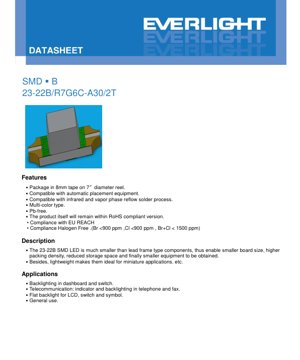
23-22B/R7G6C-A30/2T 是一款多色表面貼裝器件 (SMD) LED,專為現代緊湊型電子應用而設計。該元件在單一封裝內整合了兩種不同的芯片類型:發射深紅色的 R7 芯片和發射亮黃綠色的 G6 芯片。其主要優勢在於其微型尺寸,這有助於在印刷電路板 (PCB) 上實現更高的封裝密度,從而減小設備的整體尺寸和重量。這使其特別適合空間和重量為關鍵限制因素的應用。
The LED is packaged on 8mm tape wound onto a 7-inch diameter reel, making it fully compatible with high-speed automatic pick-and-place equipment used in volume manufacturing. It is constructed using lead-free (Pb-free) materials and complies with key environmental regulations including RoHS, EU REACH, and halogen-free standards (Br <900 ppm, Cl <900 ppm, Br+Cl < 1500 ppm). The device is also qualified for standard infrared and vapor phase reflow soldering processes.
1.1 核心優勢與目標市場
此款 SMD LED 的核心優勢源於其小巧的外形尺寸和雙色功能。其尺寸顯著小於傳統引線框架 LED,使設計師能夠創造出更緊湊的產品。減少的元件及最終組裝產品的儲存空間,帶來了物流和成本效益。其輕量化特性非常適合便攜式和微型設備。
其目標應用多樣化,主要集中於指示燈和背光功能。關鍵市場包括汽車內飾(例如儀表板和開關背光)、電信設備(例如電話和傳真機中的指示燈和背光)以及消費電子產品(例如 LCD、開關和符號的平面背光)。它亦適用於需要可靠多色信號指示的通用指示燈用途。
2. 技術參數分析
2.1 絕對最大額定值
在超出此等限值下操作器件可能會導致永久損壞。絕對最大額定值於環境溫度 (Ta) 為 25°C 時指定。
- 反向電壓 (VR): 5 V。在反向偏壓下超過此電壓可能會損壞 LED 的半導體結。
- 正向電流 (IF): R7同G6晶片嘅最大連續直流電流都係25 mA。
- 峰值正向電流 (IFP): 兩款晶片嘅峰值正向電流均為60 mA,只適用於脈衝條件(工作週期1/10 @ 1 kHz)。
- 功耗 (Pd): 每粒晶片嘅功耗為60 mW,此為封裝可承受嘅最大功率。
- 工作溫度 (Topr): -40至+85 °C。此器件適用於工業級溫度範圍。
- 儲存溫度 (Tstg): -40 至 +90 °C。
- 靜電放電 (ESD): 2000 V (人體模型)。必須遵守正確的 ESD 處理程序。
- 焊接溫度 (Tsol): 對於回流焊接,允許峰值溫度為 260°C,持續時間最長 10 秒。對於手工焊接,烙鐵頭溫度必須低於 350°C,每個端子焊接時間最長 3 秒。
2.2 電氣光學特性
除非另有說明,典型性能是在 Ta=25°C 和 IF=20mA 下測量。此封裝的典型視角 (2θ1/2) 為 130 度。
對於 R7 (深紅色) 晶片:
- 發光強度 (Iv): 範圍由 18.0 mcd (最小值) 至 72.0 mcd (最大值),典型公差為 ±11%。
- 峰值波長 (λp): 典型值為 639 nm。
- 主波長 (λd): 典型值為 631 nm。
- 頻譜帶寬 (Δλ): 通常為 20 nm。
- 正向電壓 (VF): 範圍由 1.70 V(最小)至 2.40 V(最大),典型值為 2.00 V。
適用於 G6(亮黃綠色)晶片:
- 發光強度 (Iv): 範圍由 14.5 mcd(最小)至 45.0 mcd(最大),典型公差為 ±11%。
- 峰值波長 (λp): 通常為 575 nm。
- 主波長 (λd): 通常為 573 nm。
- 頻譜帶寬 (Δλ): 通常為 20 nm。
- 正向電壓 (VF): 範圍由 1.70 V(最小)至 2.40 V(最大),典型值為 2.00 V。
通用參數:
- 反向電流 (IR): 當施加5V反向電壓時,兩顆晶片的反向電流最大值均為10 µA。
3. Binning System 解說
LED的發光強度會進行分級,以確保同一生產批次內的一致性。這讓設計師可以選取符合特定亮度要求的元件。
3.1 R7 Chip Binning
R7暗紅色LED根據其在IF=20mA下測量的發光強度,分為三個級別。
- 等級代碼1: 18.0 mcd(最小值)至28.5 mcd(最大值)
- 等級代碼2: 28.5 mcd(最小值)至45.0 mcd(最大值)
- 等級代碼3: 45.0 mcd(最小值)至72.0 mcd(最大值)
3.2 G6 Chip Binning
G6 亮黃綠色發光二極管亦分為三個等級。
- 等級代碼1: 14.5 mcd (最小值) 至 18.0 mcd (最大值)
- 等級代碼2: 18.0 mcd(最小值)至28.5 mcd(最大值)
- 等級代碼3: 28.5 mcd(最小值)至45.0 mcd(最大值)
等級代碼標示於產品包裝標籤上(位於「CAT」項下)。設計師訂購時應指定所需等級代碼,以確保其應用達到預期的亮度水平。
4. 性能曲線分析
數據表包含 R7 和 G6 芯片的典型電光特性曲線。雖然具體的圖形數據並未以文字形式提供,但這些曲線通常說明了正向電流 (IF) 與發光強度 (Iv)、正向電壓 (VF) 之間的關係,以及環境溫度對光輸出的影響。
典型曲線的主要推論: 對於兩種 LED 類型,發光強度均隨正向電流增加而增加,但並非線性關係,尤其是當電流接近最大額定值時。正向電壓具有負溫度係數,意味著它會隨著結溫升高而輕微下降。理解這些曲線對於設計合適的限流電路以及進行熱管理至關重要,以確保在整個工作溫度範圍內保持穩定的光學性能。
5. 機械與封裝資訊
5.1 封裝外形尺寸
23-22B SMD LED 具有特定的物理外形。封裝外形圖為PCB焊盤圖形設計提供了關鍵尺寸。主要尺寸包括整體長度、寬度和高度,以及焊盤的位置和大小。陰極(負極端)通常透過封裝上的標記來識別。除非另有說明,所有公差均為±0.1mm。設計師必須嚴格遵守這些尺寸,以確保正確的焊接和機械穩定性。
5.2 防潮包裝
元件以防潮敏感包裝運輸,以防止環境濕氣造成損壞。包裝包括載有LED的載帶,該載帶與乾燥劑及濕度指示卡一同置於鋁質防潮袋內。規定了捲盤尺寸和載帶凹穴尺寸,以確保與自動化組裝設備兼容。每捲包含2000件。
6. 焊接與組裝指引
6.1 儲存與處理
- 請於準備使用前才打開防潮袋。
- 開啟前:儲存於 ≤ 30°C 及 ≤ 90% 相對濕度環境中。
- 開啟後:「車間壽命」為 ≤ 30°C 及 ≤ 60% 相對濕度下1年。未使用之部件必須重新密封於乾燥包裝內。
- 如乾燥劑顯示曾暴露於濕氣或儲存時間已過,焊接前需進行烘烤處理(60 ± 5°C,24小時)。
6.2 回流焊接溫度曲線
建議採用無鉛(Pb-free)回流焊溫度曲線:
- 預熱: 150–200°C,持續60–120秒。
- 217°C(液相線)以上時間: 60–150秒。
- 峰值溫度: 最高260°C,最多持續10秒。
- 升溫速率: 最高為255°C以上每6°C/秒。
- 冷卻速率: 最高為每3°C/秒。
- 回流焊接不應進行超過兩次。
6.3 手工焊接與維修
- Use a soldering iron with a tip temperature < 350°C and capacity < 25W.
- 每個端子焊接時間限制為3秒。
- 加熱期間避免對LED施加壓力,焊接後切勿令PCB彎曲。
- 不建議焊接後進行維修。如無法避免,請使用專用雙頭焊鐵同時加熱兩個端子,並確認LED特性未有下降。
7. 封裝與訂購資料
捲盤上嘅產品標籤提供追溯及正確應用所需嘅重要資訊:
- CPN: Customer's Product Number
- 零件編號: 產品編號(例如:23-22B/R7G6C-A30/2T)
- 數量: 包裝數量(2000件/卷)
- 類別: 發光強度等級(Bin Code)
- 色調: Chromaticity Coordinates & Dominant Wavelength Rank
- 參考文獻: 正向電壓等級
- 批號: 製造批號
8. 應用設計考量
8.1 電路保護
關鍵: 必須始終使用外部限流電阻與LED串聯。其正向電壓存在一個範圍(1.7V至2.4V),且其IV特性曲線非常陡峭。若無電阻,供電電壓的微小變化便可能導致正向電流發生巨大且可能具破壞性的改變。電阻值應根據最大供電電壓和LED的最大額定正向電流,並考慮最壞情況下的正向電壓來計算。
8.2 熱管理
儘管功耗較低(60mW),但將結溫維持在規定的工作範圍內,對於長期可靠性和穩定的光輸出至關重要。應確保使用足夠的PCB銅箔面積或散熱過孔,尤其是在多個LED緊密放置在一起或環境溫度較高的情況下。
8.3 應用限制
本產品專為一般商業及工業應用而設計。未經事先諮詢及可能進行的額外認證,本產品不專門適用於高可靠性應用,例如軍事/航空航天、汽車安全/保安系統(例如安全氣囊、制動系統)或生命攸關的醫療設備。
9. 技術比較與差異
23-22B的主要差異化優勢在於其在單個極緊湊的SMD封裝內實現了多色發光能力。與使用兩個獨立的單色LED相比,它節省了PCB空間並簡化了組裝工序。兩種顏色均採用AlGaInP材料,提供了良好的發光效率和色純度。其與標準、大批量SMT製程的兼容性,使其成為量產消費類及汽車內飾電子產品的一個具成本效益的解決方案。
10. 常見問題 (FAQ)
10.1 我可以獨立驅動 R7 和 G6 晶片嗎?
可以,23-22B封裝包含兩粒電氣隔離嘅LED芯片。佢哋有獨立嘅陽極同陰極連接,可以透過獨立嘅限流電路嚟驅動。咁樣就可以實現動態混色或者獨立信號指示。
10.2 分級系統的目的是什麼?
分級係為咗確保同一生產批次內嘅亮度一致性。對於要求外觀均勻嘅應用(例如,為一排指示燈提供背光),指定並使用同一分級代碼嘅LED對於避免可見嘅亮度差異至關重要。
10.3 點解需要防潮包裝?
SMD 封裝會吸收空氣中的濕氣。在高溫回流焊接過程中,這些被困住的濕氣會迅速膨脹,導致內部分層或「爆米花」現象,使封裝破裂並損壞器件。防潮袋和乾燥劑在儲存和運輸過程中可防止此情況發生。
11. 設計與使用案例研究
場景:為網絡路由器設計多功能狀態指示燈。 設計師需要一個單一元件來顯示電源(恆亮紅色)、網絡活動(閃爍綠色)和故障狀態(紅綠交替閃爍)。23-22B 是一個理想的選擇。其細小尺寸適合有限的前面板空間。獨立的紅色(R7)和綠色(G6)晶片可通過晶體管驅動器由簡單的微控制器 GPIO 引腳控制。通過為兩種顏色指定 Bin Code 2,可以確保所有生產單位的亮度一致。設計師遵循回流焊接曲線指南,並加入適當的串聯電阻(例如,對於 5V 電源,使用 150 歐姆,按最壞情況的 Vf 計算),以確保產品在整個使用壽命期內可靠運行。
12. 操作原理
發光二極管(LED)是一種當電流通過時會發光的半導體器件。這種現象稱為電致發光。在 23-22B 中,R7 晶片採用 AlGaInP(磷化鋁鎵銦)半導體結構,優化用於發射光譜中的紅光(主波長約為 631nm)。G6 晶片使用不同成分的 AlGaInP 來發射黃綠光區域的光(約 573nm)。當施加超過晶片帶隙能量的正向電壓時,電子和電洞在半導體的有源區複合,以光子(光)的形式釋放能量。特定的材料成分決定了發射光的波長(顏色)。
13. 技術趨勢
指示燈及背光LED嘅趨勢持續邁向更高效率(每瓦電輸入產生更多光輸出)、更細封裝尺寸以提供更大設計靈活性,以及提升顏色一致性同埋隨溫度同使用壽命嘅穩定性。好似23-22B呢類多晶片封裝代表咗集成化趨勢,可以減少PCB上嘅元件數量。此外,環保合規(無鉛、無鹵)依家已經係全球法規驅動下嘅標準要求。未來發展可能包括更薄嘅封裝,以及同控制電路集成嘅「智能LED」模組。
LED 規格術語
LED技術術語完整解釋
光電性能
| 術語 | 單位/表示方式 | 簡易說明 | 重要性 |
|---|---|---|---|
| Luminous Efficacy | lm/W (lumens per watt) | 每瓦電力所產生的光輸出,數值越高代表能源效益越好。 | 直接決定能源效益級別同電費開支。 |
| 光通量 | lm (流明) | 光源發出嘅總光量,俗稱「光亮度」。 | 決定光線夠唔夠光。 |
| 視角 | ° (度),例如:120° | 光強度降至一半時嘅角度,決定光束寬度。 | 影響照明範圍同均勻度。 |
| CCT (色溫) | K (開爾文),例如:2700K/6500K | 光嘅暖感/冷感,數值越低越偏黃/暖,越高越偏白/冷。 | 決定照明氛圍與適用場景。 |
| CRI / Ra | 無單位,0–100 | 準確呈現物體顏色的能力,Ra≥80為佳。 | 影響色彩真實性,用於商場、博物館等高要求場所。 |
| SDCM | MacAdam橢圓步階,例如「5步階」 | 顏色一致性指標,步階數值越小代表顏色越一致。 | 確保同一批次LED的顏色均勻一致。 |
| Dominant Wavelength | nm(納米),例如620nm(紅色) | 對應彩色LED顏色的波長。 | 決定紅色、黃色、綠色單色LED嘅色調。 |
| Spectral Distribution | Wavelength vs intensity curve | 顯示喺唔同波長上嘅強度分佈。 | 會影響顯色性同品質。 |
電氣參數
| 術語 | 符號 | 簡易說明 | 設計考量 |
|---|---|---|---|
| 正向電壓 | Vf | 啟動LED所需的最低電壓,類似「起始閾值」。 | 驅動器電壓必須≥Vf,串聯LED的電壓會累加。 |
| 正向電流 | If | 正常LED運作時的電流值。 | Usually constant current drive, current determines brightness & lifespan. |
| 最大脈衝電流 | Ifp | 可短暫承受嘅峰值電流,用於調光或閃爍。 | Pulse width & duty cycle must be strictly controlled to avoid damage. |
| Reverse Voltage | Vr | LED可承受嘅最大反向電壓,超出可能導致擊穿。 | 電路必須防止反接或電壓尖峰。 |
| 熱阻 | Rth (°C/W) | 晶片至焊錫嘅熱傳遞阻力,數值越低越好。 | 高熱阻需要更強嘅散熱能力。 |
| ESD Immunity | V (HBM),例如:1000V | 抵禦靜電放電嘅能力,數值愈高代表愈唔易受損。 | 生產過程中需要採取防靜電措施,尤其係對於敏感嘅LED。 |
Thermal Management & Reliability
| 術語 | 關鍵指標 | 簡易說明 | 影響 |
|---|---|---|---|
| Junction Temperature | Tj (°C) | LED晶片內部實際工作溫度。 | 每降低10°C,壽命可能倍增;過高會導致光衰、色偏。 |
| Lumen Depreciation | L70 / L80 (小時) | 亮度降至初始值70%或80%所需時間。 | 直接定義LED「使用壽命」。 |
| 光通維持率 | %(例如:70%) | 經過一段時間後保留的亮度百分比。 | 表示長期使用下的亮度保持情況。 |
| Color Shift | Δu′v′ 或 MacAdam 橢圓 | 使用期間的顏色變化程度。 | 影響照明場景中的顏色一致性。 |
| Thermal Aging | Material degradation | 因長期高溫而導致的劣化。 | 可能導致亮度下降、顏色變化或開路故障。 |
Packaging & Materials
| 術語 | 常見類型 | 簡易說明 | Features & Applications |
|---|---|---|---|
| 封裝類型 | EMC, PPA, Ceramic | 外殼物料保護晶片,提供光學/熱學介面。 | EMC:良好耐熱性,成本低;陶瓷:散熱更佳,壽命更長。 |
| 晶片結構 | 正面,倒裝晶片 | 晶片電極排列。 | 倒裝晶片:散熱更佳,效能更高,適用於高功率。 |
| 螢光粉塗層 | YAG, Silicate, Nitride | 覆蓋藍色晶片,將部分轉化為黃/紅光,混合成白光。 | 不同螢光粉會影響光效、CCT及CRI。 |
| 透鏡/光學元件 | 平面、微透鏡、TIR | 控制光分佈嘅表面光學結構。 | 決定視角同光分佈曲線。 |
Quality Control & Binning
| 術語 | Binning Content | 簡易說明 | 用途 |
|---|---|---|---|
| Luminous Flux Bin | 代碼,例如 2G、2H | 按亮度分組,每組有最小/最大流明值。 | 確保同一批次亮度均勻。 |
| Voltage Bin | 代碼,例如 6W、6X | 按正向電壓範圍分組。 | 促進司機配對,提升系統效率。 |
| Color Bin | 5-step MacAdam ellipse | 按色座標分組,確保範圍緊密。 | 保證色彩一致性,避免燈具內顏色不均。 |
| CCT Bin | 2700K、3000K等 | 按相關色溫分組,每組有相應的座標範圍。 | 滿足不同場景的相關色溫要求。 |
Testing & Certification
| 術語 | Standard/Test | 簡易說明 | Significance |
|---|---|---|---|
| LM-80 | 光通維持測試 | 於恆溫下長期點亮,記錄亮度衰減。 | 用於估算LED壽命(配合TM-21)。 |
| TM-21 | 壽命估算標準 | 根據LM-80數據估算實際使用條件下的壽命。 | 提供科學化的壽命預測。 |
| IESNA | Illuminating Engineering Society | 涵蓋光學、電氣及熱學測試方法。 | 業界認可的測試基準。 |
| RoHS / REACH | 環保認證 | 確保不含對人體有害物質(鉛、汞)。 | 國際市場准入要求。 |
| ENERGY STAR / DLC | 能源效益認證 | 照明設備能源效益及性能認證。 | 適用於政府採購、資助計劃,提升競爭力。 |