目錄
- 1. 產品概述
- 1.1 核心優勢與目標市場
- 2. 深入技術參數分析
- 2.1 絕對最大額定值
- 隔離參數:
- 5. 訂購資訊與包裝
- . Performance Curve Analysis
- .1 Forward Current vs. Forward Voltage (Figure 1)
- .2 Collector Current vs. Forward Current (Figure 2) and CTR vs. Forward Current (Figure 3)
- .3 Temperature Dependence (Figures 6 & 7)
- .4 Switching Characteristics (Figure 9)
- . Mechanical, Packaging, and Assembly Information
- .1 Pin Configuration and Polarity
- .2 Soldering and Handling Guidelines
- . Ordering Information and Packaging
- . Application Guidelines and Design Considerations
- .1 Typical Application Circuits
- .2 Key Design Considerations
- . Technical Comparison and FAQs
- .1 Differentiation from Other Photocouplers
- .2 Frequently Asked Questions (FAQs)
- . Operating Principle and Technology Trends
- .1 Fundamental Operating Principle
- .2 Industry Trends
1. 產品概述
EL3H7U-G系列代表了一款緊湊型表面黏著光電晶體光耦合器家族,專為現代電子電路中可靠的訊號隔離而設計。這些元件透過光學方式在兩個隔離電路之間傳輸電氣訊號,發揮關鍵作用,從而防止一個電路中的高電壓或接地迴路影響或損壞另一個電路。
其核心結構由一個砷化鎵紅外線發光二極體與一個矽質NPN光電晶體光學耦合而成。兩者皆封裝在綠色無鹵素化合物中,並置於高度僅2.0毫米的4腳小型外型封裝內。此封裝非常適合印刷電路板上空間受限的應用。
1.1 核心優勢與目標市場
EL3H7U-G系列的主要優勢包括其高隔離能力、緊湊的外形尺寸以及符合國際安全和環境標準。其隔離電壓高達3750 Vrms,為敏感電路提供強健的保護。無鹵素材料成分符合RoHS和REACH等環保法規。本元件已獲得UL、cUL、VDE、SEMKO、NEMKO、DEMKO、FIMKO和CQC等主要國際安全機構認證,適用於需要認證元件的全球市場。
目標應用非常廣泛,主要集中在電氣隔離和抗雜訊能力至關重要的領域。關鍵市場包括交換式電源供應器、特別是DC-DC轉換器、工業可程式邏輯控制器、通訊設備,以及在不同接地電位或阻抗位準的電路之間進行通用訊號傳輸。
2. 深入技術參數分析
理解絕對最大額定值和電氣特性對於可靠的電路設計以及確保光耦合器的長期可靠性至關重要。
2.1 絕對最大額定值
這些額定值定義了可能導致元件永久損壞的應力極限,並非正常操作條件。
- 輸入端:順向電流不得超過20 mA。F逆向電壓限制為5 V,這凸顯了若輸入端可能承受逆向偏壓,則需要適當的極性保護。R輸出端:
- 集極電流額定值為30 mA。集極-射極電壓可承受高達60 V,而射極-集極電壓則低得多,僅為5 V,這顯示了光電晶體崩潰特性的不對稱性。熱與隔離:C元件總功耗為200 mW。隔離電壓3750 Vrms是在控制濕度條件下,將第1-2腳和第3-4腳分別短路後測試1分鐘的結果。工作溫度範圍指定為-40°C至+125°C。CEO2.2 電光特性ECO這些參數通常在25°C下量測,定義了元件在正常工作條件下的性能。
- 輸入特性:在順向電流為1 mA時,順向電壓典型值為1.3V,這對於驅動電路設計很重要。輸入電容最高可達250 pF,可能影響高頻切換性能。TOT輸出特性:ISO集極-射極暗電流非常低,代表LED關閉時的漏電流。集極-射極飽和電壓在指定測試條件下最大值為0.4V,表示電晶體完全導通時的電壓降很低。
隔離參數:
隔離電阻最小值為5 x 10^10 Ω,隔離電容最大值為1.0 pF。這些數值對於決定隔離屏障的共模拒斥比和高頻雜訊耦合至關重要。
- 2.3 傳輸特性與分級系統電流傳輸比是光耦合器最關鍵的參數,定義為輸出集極電流與輸入LED順向電流的比值,以百分比表示。FEL3H7U-G系列採用CTR分級系統,為設計者提供一致的性能區間:標準級、A級、B級、C級各有其CTR範圍。F這種分級允許進行更精確的設計,特別是在增益一致性很重要的電路中,例如電源供應器的回授迴路。標準零件提供最寬的範圍,適用於CTR精確度要求不高的通用應用。3. 性能曲線分析規格書提供了幾張圖表來說明關鍵性能趨勢。必須注意,這些曲線代表典型行為,並非生產測試的保證值。
- 3.1 順向電流 vs. 順向電壓此圖顯示了輸入端IRED在不同環境溫度下的I-V特性。順向電壓具有負溫度係數,這在熱管理和恆流驅動設計中必須考慮。CEO3.2 集極電流 vs. 順向電流 與 CTR vs. 順向電流CE圖2繪製了輸出集極電流與輸入LED電流的關係,顯示在較低電流時呈線性關係,但在較高電流時會飽和。圖3顯示歸一化CTR隨著LED電流增加而降低,表示元件在較低驅動電流下效率最高。3.3 溫度依賴性圖6顯示,在固定LED電流下,集極電流隨溫度升高而增加。圖7顯示歸一化CTR在室溫附近達到峰值,並在較高和較低溫度下降低。CTR的這種溫度依賴性是關鍵的設計因素。F3.4 切換特性C切換時間與負載電阻的關係圖顯示,上升時間和下降時間都隨著負載電阻減小而減少。使用較小的負載電阻可以實現更快的切換速度,但代價是輸出級功耗更高。
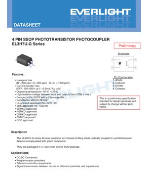
- 4. 機械、封裝與組裝資訊4.1 腳位配置與極性IO元件採用標準4腳SSOP封裝。腳位定義如下:腳位1為IRED陽極,腳位2為IRED陰極,腳位3為光電晶體射極,腳位4為光電晶體集極。在PCB佈局和組裝時必須注意正確極性以防止損壞。104.2 焊接與處理指南IO焊接溫度的絕對最大額定值為260°C持續10秒。這符合典型的無鉛迴焊製程曲線。應遵循IPC/JEDEC J-STD-020關於濕度敏感元件的標準指南。元件應儲存在原裝防潮袋中,並在受控條件下使用乾燥劑保存;若袋子已打開或超過暴露時間限制,則在焊接前應進行烘烤。
5. 訂購資訊與包裝
零件編號結構為:EL3H7U(X)(Y)-VG。其中X代表CTR等級,Y代表捲帶包裝選項,V代表可選的VDE認證標記,G代表無鹵素材料。C6. 應用指南與設計考量F6.1 典型應用電路CF主要應用是訊號隔離。典型電路涉及使用限流電阻從數位訊號源驅動輸入端LED。輸出端光電晶體可用於共射極配置以產生反相輸出訊號,或用於射極隨耦器配置以產生非反相訊號。
6.2 關鍵設計考量
- LED驅動電流:根據所需的切換速度和CTR選擇。較低的電流提供較高的CTR但切換速度較慢。必須計算串聯電阻。 輸出負載電阻:此電阻設定輸出電壓擺幅、切換速度和功耗。較小的電阻提供更快的切換速度,但輸出電壓擺幅較低且集極電流較高。 CTR衰減:光耦合器的CTR可能隨時間衰減,特別是在高溫和高LED電流下操作時。對於長壽命設計,應降低操作電流並確保充分的熱管理。 抗雜訊能力:在嘈雜環境中,在輸入端腳位靠近元件處並聯一個小型旁路電容有助於抗雜訊。對於高速訊號,仔細的PCB佈局以最小化雜散電容非常重要。7. 技術比較與常見問題F7.1 與其他光耦合器的區別CEEL3H7U-G系列透過其緊湊的SSOP封裝、高達3750 Vrms的隔離額定值、寬廣的工作溫度範圍以及全面的國際安全認證組合而與眾不同。許多競爭元件可能提供類似的CTR或速度,但缺乏完整的認證套件或高溫能力。
- 7.2 常見問題問:標準級與A/B/C級有何不同? 答:標準級具有非常寬的CTR範圍。A、B、C級被分選到更緊密、有保證的CTR範圍內。對於需要可預測增益的設計,請使用分級零件。 問:我可以用它來隔離交流輸入訊號嗎? 答:不能直接使用。輸入端是IRED,它是一個二極體,只單向導通。要隔離交流訊號,您需要先將其整流或使用專用的交流輸入光耦合器。 問:如何計算最大資料速率? 答:最大資料速率受上升時間和下降時間之和的限制。對於數位訊號,頻寬的粗略估計約為0.35除以上升時間。典型上升時間為8 μs時,頻寬約為44 kHz。對於可靠的數位通訊,實際資料速率會更低。 問:為什麼隔離電容很重要? 答:低隔離電容對於抑制高頻共模雜訊至關重要。在隔離屏障兩端有快速電壓瞬變的應用中,高隔離電容會將雜訊從初級側耦合到次級側,可能導致故障。
- 8. 工作原理與技術趨勢8.1 基本原理
- 光耦合器基於電-光-電轉換原理運作。施加到輸入端的電氣訊號使IRED發出與電流成比例的紅外光。此光線穿過封裝內的透明隔離屏障。在輸出端,光電晶體檢測到此光線,產生基極電流,進而控制更大的集極電流。兩個電路是電氣隔離的,僅透過光學耦合連接。8.2 產業趨勢
光耦合器技術的趨勢是朝向更高速度、更低功耗、更高整合度和更小封裝發展。雖然像EL3H7U-G這樣的傳統光電晶體元件非常適合直流和低頻隔離,但像數位隔離器這樣的新技術提供了顯著更高的資料速率、更低的功耗和更好的時序特性。然而,光耦合器在高共模瞬變抗擾度、簡單性以及高壓隔離方面成熟的安全認證上仍保持優勢,確保了它們在電源轉換和工業控制應用中的持續相關性。
. Performance Curve Analysis
The datasheet provides several graphs illustrating key performance trends. It is crucial to note that these curves represent typical behavior and are not guaranteed by production testing.
.1 Forward Current vs. Forward Voltage (Figure 1)
This graph shows the I-V characteristic of the input IRED at different ambient temperatures (-40°C, 25°C, 125°C). The forward voltage (VF) has a negative temperature coefficient, meaning it decreases as temperature increases for a given current. This is a typical behavior for diodes and must be considered in thermal management and constant-current drive design.
.2 Collector Current vs. Forward Current (Figure 2) and CTR vs. Forward Current (Figure 3)
Figure 2 plots the output collector current (IC) against the input LED current (IF) for two different collector-emitter voltages (VCE=0.4V and 5V). The relationship is linear at lower currents but shows saturation at higher IFlevels, especially at the lower VCE. Figure 3 shows the normalized CTR decreasing as IFincreases. This indicates that the device is most efficient (highest CTR) at lower drive currents, typically around the test condition of 0.5 mA.
.3 Temperature Dependence (Figures 6 & 7)
Figure 6 demonstrates that the collector current (IC) for a fixed IFincreases with temperature. Figure 7 shows that the normalized CTR peaks around room temperature and decreases at both higher and lower temperatures. This temperature dependence of CTR is a critical design factor. Circuits must be designed to function correctly over the entire specified temperature range, accounting for the variation in gain.
.4 Switching Characteristics (Figure 9)
The graph for switching time vs. load resistance (RL) shows that both rise time (tr) and fall time (tf) decrease as the load resistance decreases. Faster switching is achieved with smaller load resistors, but this comes at the cost of higher power dissipation in the output stage. The test circuit (Figure 13) defines tras the time from 10% to 90% of the output pulse and tfas from 90% to 10%.
. Mechanical, Packaging, and Assembly Information
.1 Pin Configuration and Polarity
The device uses a standard 4-pin SSOP footprint. The pinout is as follows: Pin 1: Anode of the IRED, Pin 2: Cathode of the IRED, Pin 3: Emitter of the phototransistor, Pin 4: Collector of the phototransistor. Correct polarity must be observed during PCB layout and assembly to prevent damage.
.2 Soldering and Handling Guidelines
The absolute maximum rating for soldering temperature (TSOL) is 260°C for 10 seconds. This aligns with typical lead-free reflow soldering profiles. Standard IPC/JEDEC J-STD-020 guidelines for moisture-sensitive devices should be followed. The device should be stored in its original moisture-barrier bag with desiccant under controlled conditions and baked before soldering if the bag has been opened or the exposure time limit is exceeded.
. Ordering Information and Packaging
The part number follows the structure: EL3H7U(X)(Y)-VG.
- X:CTR Rank (A, B, C, or blank for standard grade).
- Y:Tape and reel option (TA, TB, or blank). TA and TB likely refer to different reel sizes or packaging orientations, both containing 5000 units per reel.
- V:Optional VDE approval marking.
- G:Denotes halogen-free material.
Examples: EL3H7UB-TA-VG would be a B-grade CTR device, packaged on a TA tape and reel, with VDE approval and halogen-free material.
. Application Guidelines and Design Considerations
.1 Typical Application Circuits
The primary application is signal isolation. A typical circuit involves driving the input LED with a current-limiting resistor from a digital signal source (e.g., a microcontroller GPIO). The output phototransistor can be used in a common-emitter configuration (collector connected to a pull-up resistor, emitter grounded) to produce an inverted output signal, or in an emitter-follower configuration for a non-inverted signal.
.2 Key Design Considerations
- LED Drive Current:Select IFbased on required switching speed and CTR. Lower IFoffers higher CTR but slower switching. A series resistor must be calculated using R = (Vsource- VF) / IF.
- Output Load Resistor (RL):This resistor sets the output voltage swing, switching speed, and power dissipation. A smaller RLgives faster switching but lower output voltage swing and higher IC.
- CTR Degradation:The CTR of photocouplers can degrade over time, especially when operated at high temperatures and high LED currents. For long-life designs, derate the operating IFand ensure adequate thermal management.
- Noise Immunity:For noisy environments, a small bypass capacitor (e.g., 0.1 μF) across the input pins, close to the device, can help. On the output, careful PCB layout to minimize stray capacitance is important for high-speed signals.
. Technical Comparison and FAQs
.1 Differentiation from Other Photocouplers
The EL3H7U-G series differentiates itself through its combination of a compact SSOP package, high 3750 Vrms isolation rating, wide -40°C to +125°C operating temperature, and comprehensive international safety certifications. Many competing devices may offer similar CTR or speed but lack the full suite of approvals or the high-temperature capability.
.2 Frequently Asked Questions (FAQs)
Q: What is the difference between the standard grade and the A/B/C grades?
A: The standard grade has a very wide CTR range (50-600%). The A, B, and C grades are binned into tighter, guaranteed CTR ranges (e.g., 200-400% for C-grade). Use graded parts for designs requiring predictable gain.
Q: Can I use this for AC input signal isolation?
A: Not directly. The input is an IRED, which is a diode and only conducts in one direction. To isolate an AC signal, you would need to first rectify it or use a dedicated AC-input photocoupler.
Q: How do I calculate the maximum data rate?
A>The maximum data rate is limited by the sum of the rise and fall times (tr+ tf). A rough estimate for a digital signal is Bandwidth ≈ 0.35 / (tr). With typical trof 8 μs, the bandwidth is about 44 kHz. For reliable digital communication, the practical data rate will be lower.
Q: Why is the isolation capacitance important?
A: Low isolation capacitance (CIO) is crucial for rejecting high-frequency common-mode noise. In applications with fast voltage transients across the isolation barrier (like in motor drives), a high CIOcan couple noise from the primary to the secondary side, potentially causing malfunctions.
. Operating Principle and Technology Trends
.1 Fundamental Operating Principle
A photocoupler operates on the principle of electro-optical-electrical conversion. An electrical signal applied to the input side causes the IRED to emit infrared light proportional to the current. This light traverses a transparent isolation barrier within the package. On the output side, the phototransistor detects this light, generating a base current which in turn controls a much larger collector current. The two circuits are electrically isolated, with only optical coupling between them.
.2 Industry Trends
The trend in photocoupler technology is towards higher speed, lower power consumption, higher integration, and smaller packages. While traditional phototransistor-based devices like the EL3H7U-G are excellent for DC and low-frequency isolation, newer technologies like digital isolators (using CMOS and RF or capacitive coupling) offer significantly higher data rates, lower power, and better timing characteristics. However, photocouplers maintain advantages in high common-mode transient immunity (CMTI), simplicity, and well-established safety certifications for high-voltage isolation, ensuring their continued relevance in power conversion and industrial control applications.
LED規格術語詳解
LED技術術語完整解釋
一、光電性能核心指標
| 術語 | 單位/表示 | 通俗解釋 | 為什麼重要 |
|---|---|---|---|
| 光效(Luminous Efficacy) | lm/W(流明/瓦) | 每瓦電能發出的光通量,越高越節能。 | 直接決定燈具的能效等級與電費成本。 |
| 光通量(Luminous Flux) | lm(流明) | 光源發出的總光量,俗稱"亮度"。 | 決定燈具夠不夠亮。 |
| 發光角度(Viewing Angle) | °(度),如120° | 光強降至一半時的角度,決定光束寬窄。 | 影響光照範圍與均勻度。 |
| 色溫(CCT) | K(開爾文),如2700K/6500K | 光的顏色冷暖,低值偏黃/暖,高值偏白/冷。 | 決定照明氛圍與適用場景。 |
| 顯色指數(CRI / Ra) | 無單位,0–100 | 光源還原物體真實顏色的能力,Ra≥80為佳。 | 影響色彩真實性,用於商場、美術館等高要求場所。 |
| 色容差(SDCM) | 麥克亞當橢圓步數,如"5-step" | 顏色一致性的量化指標,步數越小顏色越一致。 | 保證同一批燈具顏色無差異。 |
| 主波長(Dominant Wavelength) | nm(奈米),如620nm(紅) | 彩色LED顏色對應的波長值。 | 決定紅、黃、綠等單色LED的色相。 |
| 光譜分佈(Spectral Distribution) | 波長 vs. 強度曲線 | 顯示LED發出的光在各波長的強度分佈。 | 影響顯色性與顏色品質。 |
二、電氣參數
| 術語 | 符號 | 通俗解釋 | 設計注意事項 |
|---|---|---|---|
| 順向電壓(Forward Voltage) | Vf | LED點亮所需的最小電壓,類似"啟動門檻"。 | 驅動電源電壓需≥Vf,多個LED串聯時電壓累加。 |
| 順向電流(Forward Current) | If | 使LED正常發光的電流值。 | 常採用恆流驅動,電流決定亮度與壽命。 |
| 最大脈衝電流(Pulse Current) | Ifp | 短時間內可承受的峰值電流,用於調光或閃光。 | 脈衝寬度與佔空比需嚴格控制,否則過熱損壞。 |
| 反向電壓(Reverse Voltage) | Vr | LED能承受的最大反向電壓,超過則可能擊穿。 | 電路中需防止反接或電壓衝擊。 |
| 熱阻(Thermal Resistance) | Rth(°C/W) | 熱量從晶片傳到焊點的阻力,值越低散熱越好。 | 高熱阻需更強散熱設計,否則結溫升高。 |
| 靜電放電耐受(ESD Immunity) | V(HBM),如1000V | 抗靜電打擊能力,值越高越不易被靜電損壞。 | 生產中需做好防靜電措施,尤其高靈敏度LED。 |
三、熱管理與可靠性
| 術語 | 關鍵指標 | 通俗解釋 | 影響 |
|---|---|---|---|
| 結溫(Junction Temperature) | Tj(°C) | LED晶片內部的實際工作溫度。 | 每降低10°C,壽命可能延長一倍;過高導致光衰、色漂移。 |
| 光衰(Lumen Depreciation) | L70 / L80(小時) | 亮度降至初始值70%或80%所需時間。 | 直接定義LED的"使用壽命"。 |
| 流明維持率(Lumen Maintenance) | %(如70%) | 使用一段時間後剩餘亮度的百分比。 | 表徵長期使用後的亮度保持能力。 |
| 色漂移(Color Shift) | Δu′v′ 或 麥克亞當橢圓 | 使用過程中顏色的變化程度。 | 影響照明場景的顏色一致性。 |
| 熱老化(Thermal Aging) | 材料性能下降 | 因長期高溫導致的封裝材料劣化。 | 可能導致亮度下降、顏色變化或開路失效。 |
四、封裝與材料
| 術語 | 常見類型 | 通俗解釋 | 特點與應用 |
|---|---|---|---|
| 封裝類型 | EMC、PPA、陶瓷 | 保護晶片並提供光學、熱學介面的外殼材料。 | EMC耐熱好、成本低;陶瓷散熱優、壽命長。 |
| 晶片結構 | 正裝、倒裝(Flip Chip) | 晶片電極佈置方式。 | 倒裝散熱更好、光效更高,適用於高功率。 |
| 螢光粉塗層 | YAG、矽酸鹽、氮化物 | 覆蓋在藍光晶片上,部分轉化為黃/紅光,混合成白光。 | 不同螢光粉影響光效、色溫與顯色性。 |
| 透鏡/光學設計 | 平面、微透鏡、全反射 | 封裝表面的光學結構,控制光線分佈。 | 決定發光角度與配光曲線。 |
五、質量控制與分檔
| 術語 | 分檔內容 | 通俗解釋 | 目的 |
|---|---|---|---|
| 光通量分檔 | 代碼如 2G、2H | 按亮度高低分組,每組有最小/最大流明值。 | 確保同一批產品亮度一致。 |
| 電壓分檔 | 代碼如 6W、6X | 按順向電壓範圍分組。 | 便於驅動電源匹配,提高系統效率。 |
| 色區分檔 | 5-step MacAdam橢圓 | 按顏色坐標分組,確保顏色落在極小範圍內。 | 保證顏色一致性,避免同一燈具內顏色不均。 |
| 色溫分檔 | 2700K、3000K等 | 按色溫分組,每組有對應的坐標範圍。 | 滿足不同場景的色溫需求。 |
六、測試與認證
| 術語 | 標準/測試 | 通俗解釋 | 意義 |
|---|---|---|---|
| LM-80 | 流明維持測試 | 在恆溫條件下長期點亮,記錄亮度衰減數據。 | 用於推算LED壽命(結合TM-21)。 |
| TM-21 | 壽命推演標準 | 基於LM-80數據推算實際使用條件下的壽命。 | 提供科學的壽命預測。 |
| IESNA標準 | 照明工程學會標準 | 涵蓋光學、電氣、熱學測試方法。 | 行業公認的測試依據。 |
| RoHS / REACH | 環保認證 | 確保產品不含有害物質(如鉛、汞)。 | 進入國際市場的准入條件。 |
| ENERGY STAR / DLC | 能效認證 | 針對照明產品的能效與性能認證。 | 常用於政府採購、補貼項目,提升市場競爭力。 |