目錄
- 1. 產品概述
- 1.1 目標應用
- 2. 技術參數深度解析
- 2.1 Absolute Maximum Ratings
- 2.2 電氣光學特性
- 3. 分級系統說明
- 3.1 輻射通量分級
- 3.2 峰值波長分檔
- 3.3 順向電壓分檔
- 4. 性能曲線分析
- 4.1 順向電壓 vs. 順向電流 (IV 曲線)
- 4.2 相對輻射通量 vs. 順向電流
- 4.3 相對輻射通量 vs. 接面溫度
- 4.4 峰值波長 vs. 接面溫度
- 4.5 光譜分佈
- 4.6 降額曲線
- 5. 機械與封裝資訊
- 5.1 機械尺寸
- 5.2 焊墊設計與極性
- 6. 銲接與組裝指南
- 6.1 迴流焊接製程
- 7. 封裝與訂購資訊
- 7.1 發射極帶狀與捲盤封裝
- 7.2 濕度敏感度與儲存條件
- 7.3 產品命名規則 (訂購代碼)
- 7.4 標籤說明
- 8. 應用建議與設計考量
- 8.1 熱管理
- 8.2 電氣驅動
- 8.3 光學設計
- 9. 技術比較與差異化
- 10. 常見問題(基於技術參數)
- 10.1 輻射通量(mW)與光通量(lm)有何不同?
- 10.2 為何需要恆流驅動器?
- 10.3 我可以將此LED驅動至其最大電流120mA嗎?
- 10.4 訂購時應如何解讀分級代碼?
- 11. 設計與使用案例研究
- 11.1 案例:便攜式紫外線防偽檢測儀
- 12. 技術原理介紹
- 13. 技術趨勢
1. 產品概述
本文件提供一系列採用緊湊型表面黏著元件(SMD)封裝的高性能紫外線A(UVA)發光二極體(LED)之完整技術規格。此類元件主要應用於需要在365-370奈米波長範圍內進行受控紫外線發射的系統。
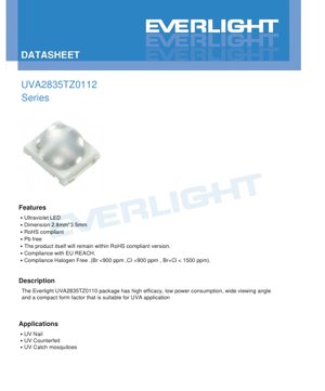
此產品系列的核心優勢包括高輻射效能(意味著每單位電能輸入可產生更多光學輸出)以及低功耗特性。該元件具備120度的寬視角,確保在目標應用中能實現廣泛且均勻的照射。其外形尺寸為長2.8毫米、寬3.5毫米,適合整合到空間受限的現代電子組件中。
The product is designed to comply with major international environmental and safety standards. It is confirmed to be RoHS (Restriction of Hazardous Substances) compliant, is manufactured using lead-free (Pb-free) processes, and adheres to the EU REACH regulation. Furthermore, it meets halogen-free requirements, with bromine (Br) and chlorine (Cl) content kept below specified limits (Br <900ppm, Cl <900ppm, Br+Cl <1500ppm).
1.1 目標應用
特定的波長與輸出特性使此LED系列成為多種利基應用的理想選擇:
- UV美甲固化: 用於固化凝膠指甲油的設備中。
- UV防偽檢測: 應用於掃描器和檢測器,以顯示在UVA光下會產生螢光的鈔票、文件或產品上的安全特徵。
- UV捕蚊燈: 整合於捕蟲裝置中,利用UVA光線吸引飛蟲。
2. 技術參數深度解析
2.1 Absolute Maximum Ratings
這些額定值定義了可能導致設備永久損壞的極限。在此條件下操作不保證正常運行。
- 最大直流正向電流 (IF): 120 mA
- 最大靜電放電耐受度(人體模型): 2000 V
- 熱阻(Rth): 25 °C/W。此參數表示熱量從LED接面傳遞至焊墊的效率。數值越低,散熱管理效果越好。
- Maximum Junction Temperature (TJ): 110 °C。半導體晶片本身的溫度不得超過此限制。
- Operating Temperature Range (TOpr): -40 °C 至 +85 °C。
- Storage Temperature Range (TStg): -40 °C 至 +100 °C。
2.2 電氣光學特性
所列訂單代碼的典型工作點與性能定義如下。除非另有說明,所有測量通常均在焊盤溫度為 25°C 下進行。
- 順向電流 (IF): 60 mA (典型工作點)
- 順向電壓 (VF): 3.2 V 至 3.8 V (於 IF = 60mA)
- 峰值波長 (λP): 365 nm 至 370 nm
- 輻射通量 (Φe):
- 最小值:70 mW
- 典型值:90 mW
- 最大值:130 mW
3. 分級系統說明
為確保量產的一致性,LED會根據性能進行分檔。這讓設計師能為其應用選擇符合特定最低標準的元件。
3.1 輻射通量分級
LED 根據其在工作電流下的最小輻射通量輸出進行分類。分級代碼 (R5, R6, R7, R8, R9, S1) 代表遞增的輸出水平,從最低 70mW (R5) 到最高 130mW (S1)。量測容差為 ±10%。
3.2 峰值波長分檔
波長受到嚴格控制。此系列中的所有裝置均歸屬於單一分類標籤「U36」,確保峰值波長介於365nm至370nm之間,測量公差為±1nm。
3.3 順向電壓分檔
裝置亦根據其在60mA下的順向壓降進行分類。定義了三個分選等級:
- 3234: VF = 3.2V - 3.4V
- 3436: VF = 3.4V - 3.6V
- 3638: VF = 3.6V - 3.8V
4. 性能曲線分析
4.1 順向電壓 vs. 順向電流 (IV 曲線)
所提供的曲線闡明了施加於LED兩端的電壓與所產生電流之間的非線性關係。對於設定為60mA的恆流驅動器,預期的壓降將落在電氣特性中定義的3.2V-3.8V範圍內。該曲線顯示了電壓如何隨電流增加而上升,強調了需要透過適當的電流調節(而非電壓調節)來控制光輸出並防止熱失控。
4.2 相對輻射通量 vs. 順向電流
此圖表說明光學輸出(輻射通量)大致與順向電流成正比。增加驅動電流將提高光輸出。然而,在建議的60mA以上運作將產生更多熱量,可能降低效能並縮短使用壽命,如降額曲線所示。
4.3 相對輻射通量 vs. 接面溫度
這是熱管理的一項關鍵特性。該曲線顯示,隨著接面溫度 (TJ) 升高,輻射通量輸出會降低。此負溫度係數凸顯了有效熱設計(例如,使用帶有散熱孔、足夠銅箔面積,並可能搭配散熱片的PCB)的重要性,以在運作期間盡可能維持LED的接面溫度處於低點,從而確保穩定且最大的光輸出。
4.4 峰值波長 vs. 接面溫度
LED的峰值發射波長對溫度有輕微的依賴性。此圖量化了此UVA元件的波長偏移。理解此偏移對於波長精度至關重要的應用非常重要,例如在某些固化或螢光製程中。
4.5 光譜分佈
相對光譜分佈圖顯示了不同波長下所發射的光強度。對於此UVA LED,其發射光譜以365-370奈米波峰為中心,並具有特徵光譜寬度。此資訊對於對特定紫外光譜波段敏感的應用至關重要。
4.6 降額曲線
降額曲線根據在焊盤(陽極側)測量到的溫度,提供了最大允許連續正向電流。隨著焊盤溫度升高,必須降低最大安全工作電流,以防止超過110°C的最高接面溫度。此曲線對於設計可靠的系統至關重要,特別是在高環境溫度的應用中。
5. 機械與封裝資訊
5.1 機械尺寸
LED封裝的矩形佔位面積為2.8mm x 3.5mm。詳細尺寸圖明確規定了焊墊的精確位置、透鏡幾何形狀以及散熱墊的位置。散熱墊註明與陰極電氣連接。除非另有說明,標準尺寸公差為±0.2mm。一項關鍵操作注意事項警告勿對透鏡施力,否則可能導致元件故障。
5.2 焊墊設計與極性
焊接圖案設計圖明確標示了陽極與陰極焊墊。組裝時必須遵守正確的極性。該設計包含一個中央散熱墊,以促進熱量從LED晶片傳導至印刷電路板(PCB)。
6. 銲接與組裝指南
6.1 迴流焊接製程
此UVA LED系列適用於標準表面貼裝技術(SMT)組裝製程。關鍵指引包含:
- 為避免熱應力,同一元件不應執行超過兩次迴流焊接。
- 焊接加熱階段必須盡量減少對LED本體的機械應力。
- 發光二極體焊接完成後,電路板不應彎曲或扭曲。
- 若使用黏著劑,其固化過程必須遵循與元件相容的標準烘烤溫度曲線。
建議採用典型的迴流焊溫度曲線,圖示預熱、保溫、迴流及冷卻階段建議的時間-溫度關係,以確保焊點可靠且不損壞LED。
7. 封裝與訂購資訊
7.1 發射極帶狀與捲盤封裝
為實現自動化取放組裝,LED以壓紋載帶包裝並捲繞於捲盤上供應。標準包裝數量為每捲盤2000顆。提供載帶凹槽及捲盤本身的詳細尺寸圖,典型公差為±0.1mm。
7.2 濕度敏感度與儲存條件
元件採用防潮阻隔袋包裝,以防止吸收大氣中的濕氣,這可能在高溫回焊過程中導致「爆米花現象」(封裝破裂)。一旦密封袋被打開,元件應在指定時間內使用,或根據標準 IPC/JEDEC 指南在焊接前進行烘烤。
7.3 產品命名規則 (訂購代碼)
完整的訂購代碼是一個結構化字串,用以編碼所有關鍵規格。例如: UVA2835TZ0112-PUA6570120X38060-2T 細分如下:
- UVA2835TZ0112: 基礎料號 (UVA, 2835封裝, PCT材質, 含齊納二極體, 1晶片, 120°發光角度).
- P: 晶片方向 (P面朝上).
- UA: 色彩渲染指數代碼 (UVA)。
- 6570: 波長範圍代碼。
- 120: 最大輻射通量規格代碼。
- X38: 順向電壓範圍 (3.2V-3.8V)。
- 060: 順向電流額定值 (60mA)。
- 2: 包裝類型(每捲2,000片)。
- T: 捲帶包裝代碼。
7.4 標籤說明
捲盤標籤包含數個用於追溯與識別的欄位:
- P/N: 製造商的生產編號。
- 數量: 捲盤上的元件數量。
- CAT / HUE / REF: 分別代表輻射通量區間、顏色(波長)區間與順向電壓區間的代碼。
- LOT No: 用於追溯的生產批號。
8. 應用建議與設計考量
8.1 熱管理
考慮到25°C/W的熱阻以及溫度對輸出功率和波長的負面影響,有效的散熱設計至關重要。設計人員應:
- 使用具有專用散熱焊盤連接至內部接地層或大面積銅箔的PCB。
- 在LED的散熱焊盤下方設置多個散熱通孔,以將熱量傳導至其他PCB層或外部散熱器。
- 請參考降額曲線,以確保操作電流適用於應用中預期的最高焊墊溫度。
8.2 電氣驅動
LED是電流驅動元件。強烈建議使用恆流驅動電路,而非簡單的串聯電阻或電壓源,特別是在需要穩定輸出與長使用壽命的應用中。驅動器應設計為提供穩定的60mA電流(或根據降額要求使用更低電流),且必須能承受3.2V至3.8V的正向電壓範圍。
8.3 光學設計
120度的視角可提供寬廣的光束。對於需要聚焦或準直UV光的應用,必須使用二次光學元件(如透鏡或反射器)。此類光學元件的材質必須對UVA波長具透光性(例如特殊玻璃或UV穩定塑料如PMMA)。
9. 技術比較與差異化
相較於舊式的穿孔式UV燈或較大的SMD封裝,此款2835 UVA LED具有顯著優勢:
- 尺寸與整合性: 緊湊的2835封裝尺寸允許更高密度的佈局,並能整合到更小巧的現代裝置中。
- 效率: 高輻射效能意味著在特定光輸出下,能降低功耗並減少熱量產生。
- 使用壽命: 固態LED通常比傳統UV燈泡擁有更長的操作壽命。
- 即時開關: LED可立即達到全輸出亮度,不像某些燈泡需要預熱時間。
- 環境: 符合RoHS、無鹵素與REACH規範,滿足全球嚴格的環境法規要求。
10. 常見問題(基於技術參數)
10.1 輻射通量(mW)與光通量(lm)有何不同?
光通量(以流明為單位)是根據人眼敏感度(明視覺)加權計算的。輻射通量(以瓦特為單位)則是發射出的總光功率,與可見度無關。由於UVA光對人眼基本上不可見,因此其性能正確地以輻射通量(mW)來表示。
10.2 為何需要恆流驅動器?
LED的正向電壓會隨溫度和個體差異而變化(如分檔所示)。恆定電壓源會導致電流大幅波動,造成光輸出不一致及潛在的過電流損壞。恆定電流源則能確保穩定、可預測的性能。
10.3 我可以將此LED驅動至其最大電流120mA嗎?
絕對最大額定值120mA是應力極限,並非建議工作條件。在此電流下連續運作會產生過多熱量,除非使用特殊的冷卻方案,否則很可能超過最大接面溫度。建議工作電流為60mA,如電氣特性表所定義。任何高於室溫的操作都必須參考降額曲線。
10.4 訂購時應如何解讀分級代碼?
請根據您應用的最低要求選擇分級。例如,若您的系統需要至少90mW的紫外線輸出,您應指定R7、R8、R9或S1分級。若您的驅動電路有嚴格的電壓限制,您可能需要指定特定的順向電壓分級(例如3234)。完整訂購代碼將包含這些分級選擇。
11. 設計與使用案例研究
11.1 案例:便攜式紫外線防偽檢測儀
設計目標: 創建一個手持式、電池供電的貨幣檢查裝置。
實作方式: 一個由3.7V鋰離子電池供電的小型高效升壓轉換器/恆流驅動器,可串聯驅動4至6個此類UVA LED。其120°的寬廣光束角消除了對複雜光學元件的需求,允許將其簡單置於紫外透射窗後方。緊湊的2835封裝尺寸使PCB保持小巧。由於此類裝置通常為間歇性短時間使用,散熱管理在此不那麼關鍵。設計師會選擇特定的輻射通量等級(例如R7或更高),以確保足夠的照度。
12. 技術原理介紹
UVA LED基於半導體材料中的電致發光原理運作。當在LED晶片的p-n接面施加正向電壓時,電子和電洞在發光層複合,以光子的形式釋放能量。這些光子的特定波長(此處為365-370奈米)由晶片結構中所用半導體材料(通常涉及氮化鋁鎵或類似III族氮化物)的能隙決定。發射出的UVA輻射人眼不可見,但能導致某些材料產生螢光並引發光化學反應,此為其在固化與檢測應用中的基礎。
13. 技術趨勢
UV LED 領域正快速發展。主要趨勢包括:
- 提升效能: 持續的研究旨在提升UVA LED的電光轉換效率(光功率輸出/電功率輸入),以降低能耗與熱負荷。
- 更短波長: 持續開發可靠且高效的UVB和UVC LED,應用於殺菌、醫療治療和感測領域。
- 更高功率密度: 晶片設計和封裝熱管理技術的改進,使單一元件能實現更高的輻射通量輸出。
- 提升使用壽命與可靠性: 材料與封裝技術的進步,正不斷延長UV LED的運作壽命,使其能夠勝任更嚴苛的工業應用。
- 成本降低: 隨著製造量提升與製程成熟,每毫瓦紫外光輸出的成本持續下降,從而開拓了新的市場應用。
LED 規格術語
LED 技術術語完整解說
光電性能
| Term | Unit/Representation | 簡易說明 | 重要性 |
|---|---|---|---|
| Luminous Efficacy | lm/W (流明每瓦) | 每瓦電力的光輸出,數值越高代表能源效率越好。 | 直接決定能源效率等級與電費成本。 |
| 光通量 | lm (lumens) | 光源發出的總光量,通常稱為「亮度」。 | 決定光線是否足夠明亮。 |
| 視角 | ° (度),例如:120° | 光強度降至一半時的角度,決定光束寬度。 | 影響照明範圍與均勻度。 |
| CCT (Color Temperature) | K (Kelvin),例如 2700K/6500K | 光線的暖/冷色調,數值越低越偏黃/暖,越高越偏白/冷。 | 決定照明氛圍與適用場景。 |
| CRI / Ra | 無單位,0–100 | 能夠準確呈現物體色彩的能力,Ra≥80即為良好。 | 影響色彩真實性,用於商場、博物館等高要求場所。 |
| SDCM | MacAdam橢圓步階,例如「5步階」 | 色彩一致性指標,步階數值越小代表色彩一致性越高。 | 確保同一批次LED的顏色均勻一致。 |
| Dominant Wavelength | nm (nanometers), e.g., 620nm (red) | 對應彩色LED顏色的波長。 | 決定紅色、黃色、綠色單色LED的色調。 |
| 光譜分佈 | 波長對強度曲線 | 顯示強度在波長上的分佈。 | 影響色彩呈現與品質。 |
Electrical Parameters
| Term | Symbol | 簡易說明 | 設計考量 |
|---|---|---|---|
| Forward Voltage | Vf | 點亮LED所需的最低電壓,類似「啟動閾值」。 | 驅動器電壓必須 ≥Vf,串聯LED的電壓會累加。 |
| Forward Current | If | 正常LED運作時的電流值。 | Usually constant current drive, current determines brightness & lifespan. |
| 最大脈衝電流 | Ifp | 可耐受短時間的峰值電流,用於調光或閃爍。 | Pulse width & duty cycle must be strictly controlled to avoid damage. |
| Reverse Voltage | Vr | LED可承受的最大反向電壓,超過此值可能導致擊穿。 | 電路必須防止反接或電壓突波。 |
| Thermal Resistance | Rth (°C/W) | 晶片至焊料的熱傳導阻力,數值越低越好。 | 高熱阻需要更強的散熱能力。 |
| ESD Immunity | V (HBM),例如:1000V | 承受靜電放電的能力,數值越高表示越不易受損。 | 生產過程中需要採取防靜電措施,特別是對於敏感的LED元件。 |
Thermal Management & Reliability
| Term | Key Metric | 簡易說明 | 影響 |
|---|---|---|---|
| Junction Temperature | Tj (°C) | LED晶片內部實際工作溫度。 | 每降低10°C可能使壽命倍增;過高則會導致光衰、色偏。 |
| 光通量衰減 | L70 / L80 (小時) | 亮度降至初始值70%或80%所需時間。 | 直接定義LED的「使用壽命」。 |
| Lumen Maintenance | % (例如:70%) | 經過一段時間後所保留的亮度百分比。 | 表示長期使用下的亮度保持能力。 |
| 色偏移 | Δu′v′ or MacAdam ellipse | 使用期間的顏色變化程度。 | 影響照明場景中的顏色一致性。 |
| 熱老化 | 材料劣化 | 因長期高溫導致的劣化。 | 可能導致亮度下降、顏色變化或開路故障。 |
Packaging & Materials
| Term | 常見類型 | 簡易說明 | Features & Applications |
|---|---|---|---|
| Package Type | EMC, PPA, Ceramic | 保護晶片的外殼材料,提供光學/熱介面。 | EMC:良好的耐熱性,成本較低;陶瓷:散熱效果更佳,使用壽命更長。 |
| Chip Structure | Front, Flip Chip | 晶片電極排列。 | 覆晶封裝:散熱更佳、效能更高,適用於高功率。 |
| 螢光粉塗層 | YAG, Silicate, Nitride | 覆蓋藍光晶片,將部分轉換為黃/紅光,混合成白光。 | 不同的螢光粉會影響光效、色溫和顯色指數。 |
| Lens/Optics | 平面、微透鏡、全內反射 | 表面光學結構控制光線分佈。 | 決定視角與光分佈曲線。 |
Quality Control & Binning
| Term | Binning Content | 簡易說明 | 目的 |
|---|---|---|---|
| 光通量分檔 | Code e.g., 2G, 2H | 依亮度分組,每組有最小/最大流明值。 | 確保同一批次亮度均勻。 |
| 電壓分級 | 代碼,例如 6W, 6X | 依順向電壓範圍分組。 | 便於驅動器匹配,提升系統效率。 |
| Color Bin | 5階麥克亞當橢圓 | 依據色座標分組,確保緊密範圍。 | 保證色彩一致性,避免燈具內部顏色不均。 |
| CCT Bin | 2700K, 3000K etc. | 依據CCT分組,每組皆有對應的座標範圍。 | 滿足不同場景的CCT需求。 |
Testing & Certification
| Term | Standard/Test | 簡易說明 | 重要性 |
|---|---|---|---|
| LM-80 | 光通維持率測試 | 恆溫長期點燈,記錄亮度衰減。 | 用於估算LED壽命(配合TM-21)。 |
| TM-21 | 壽命評估標準 | 依據LM-80數據估算實際條件下的壽命。 | 提供科學的壽命預測。 |
| IESNA | Illuminating Engineering Society | 涵蓋光學、電氣、熱學測試方法。 | 業界公認的測試基準。 |
| RoHS / REACH | 環境認證 | 確保不含危害物質(鉛、汞)。 | 國際市場准入要求。 |
| ENERGY STAR / DLC | 能源效率認證 | 照明設備的能源效率與性能認證。 | 用於政府採購、補貼計畫,提升競爭力。 |