Table of Contents
- 1. Product Overview
- 1.1 Core Advantages and Target Market
- 2. In-Depth Technical Parameter Analysis
- 2.1 Absolute Maximum Ratings
- 2.2 Electrical Characteristics
- 2.3 Transfer Characteristics
- 3. Grading System Explanation
- 4. Performance Curve Analysis
- 5. Mechanical and Package Information
- 6. Soldering and Assembly Guidelines
- 7. Ordering and Packaging Information
- 8. Application Recommendations
- 8.1 Typical Application Circuits
- 8.2 Design Considerations
- 9. Technical Comparison and Differentiation
- 10. Frequently Asked Questions (FAQ)
- 11. Practical Design Case Study
- 12. Operating Principle
- 13. Technology Trends
- LED Specification Terminology
- Photoelectric Performance
- Electrical Parameters
- Thermal Management & Reliability
- Packaging & Materials
- Quality Control & Binning
- Testing & Certification
1. Product Overview
The CNY64S series represents a family of high-performance photocouplers (opto-isolators) designed for applications demanding robust electrical isolation and reliable signal transmission. At its core, the device consists of an infrared Gallium Arsenide (GaAs) light-emitting diode (LED) optically coupled to a silicon NPN phototransistor. This configuration allows for the transfer of electrical signals between two circuits while maintaining a high degree of electrical isolation, preventing ground loops, noise transmission, and high-voltage surges from damaging sensitive components.
The primary design objective of the CNY64S series is to provide reinforced safety isolation. This is achieved through a combination of a substantial creepage and clearance distance (ensured by a package with a through-insulation thickness of ≥3mm) and high dielectric strength materials. The device is housed in a compact 4-pin Dual In-line Package (DIP), which is a through-hole mounting style, offering mechanical stability and ease of manual or wave soldering processes. The series is characterized by its very high isolation voltage ratings, making it suitable for industrial, power supply, and medical equipment where user safety and system integrity are paramount.
1.1 Core Advantages and Target Market
The key advantages of the CNY64S photocoupler stem from its safety-oriented design and reliable performance parameters.
- Exceptional Isolation: With a maximum transient isolation voltage (VIOTM) of 8200V peak for the standard version and 10000V peak for the VDE-approved "-V" variant, it offers superior protection against high-voltage transients. The rated repetitive peak isolation voltage (VIORM) is 2200V.
- High Voltage Capability: The output phototransistor has a minimum Collector-Emitter breakdown voltage (BVCEO) of 80V, allowing it to interface directly with higher voltage circuits without additional buffering in many cases.
- Safety Certifications: The device is approved by major international safety standards bodies including CUL, VDE, and FIMKO. The VDE approval specifically certifies it for reinforced isolation according to DIN EN 60747-5-5, a critical requirement for safety-critical applications.
- Environmental Compliance: It is manufactured to be lead-free (Pb-free) and compliant with the RoHS (Restriction of Hazardous Substances) directive.
- Wide Operating Range: It functions reliably across an extended temperature range from -55°C to +85°C.
The target market for the CNY64S includes designers of Switch Mode Power Supplies (SMPS) for feedback loop isolation, industrial automation systems (PLC I/O, motor drives), medical equipment requiring patient isolation, telecommunications equipment, and any microprocessor-based system where signals must cross different voltage domains or safety boundaries safely.
2. In-Depth Technical Parameter Analysis
A thorough understanding of the electrical and optical parameters is essential for proper circuit design and ensuring long-term reliability.
2.1 Absolute Maximum Ratings
These ratings define the stress limits beyond which permanent damage to the device may occur. They are not intended for normal operation.
- Input (LED): The maximum continuous forward current (IF) is 75 mA. A short-duration peak current (IFM) of 1.5A for less than 10µs is permissible. The absolute maximum reverse voltage (VR) is only 5V, highlighting the LED's sensitivity to reverse bias. Exceeding this can quickly degrade the LED. The input power dissipation (PD) must not exceed 120 mW.
- Output (Phototransistor): The maximum continuous collector current (IC) is 50 mA. The collector power dissipation (PC) limit is 150 mW. The Collector-Emitter voltage (VCEO) must stay below 80V, and the Emitter-Collector voltage (VECO) below 7V.
- Device Limits: The total device power dissipation (Ptot) is 250 mW. The isolation voltage (Viso) is tested at 8200 VRMS for one minute under controlled humidity (40-60% RH).
2.2 Electrical Characteristics
These parameters are guaranteed under specified test conditions and define the device's performance.
- Input Characteristics: At a forward current of 50mA, the LED forward voltage (VF) is typically 1.6V with a maximum of 2.0V. This is important for calculating the current-limiting resistor value. The reverse leakage current (IR) is very low (<10 µA at 5V).
- Output Characteristics: The dark current (ICEO), which is the leakage current of the phototransistor when the LED is off, is a maximum of 200 nA at VCE=20V. This parameter is crucial for determining the off-state signal integrity and noise floor. The collector-emitter saturation voltage (VCE(sat)) is a maximum of 0.3V when the transistor is fully on (IF=10mA, IC=1mA), indicating good switching performance.
- Isolation Characteristics: The coupling capacitance (CIO) is typically a very low 0.3 pF, which minimizes capacitive coupling of high-frequency noise across the isolation barrier. The isolation resistance (RIO) is a minimum of 1011 Ω (100 GΩ) at 500V DC, representing an excellent DC insulation property.
2.3 Transfer Characteristics
This is the heart of the photocoupler's functionality, defining the relationship between input current and output current.
- Current Transfer Ratio (CTR): This is the ratio of output collector current (IC) to input LED forward current (IF), expressed as a percentage (CTR = IC / IF * 100%). The CNY64S series is offered in three CTR grades or "ranks":
- CNY64S: CTR range from 50% to 300%.
- CNY64SA: CTR range from 63% to 125%.
- CNY64SB: CTR range from 100% to 200%.
The CTR is measured under standard conditions (IF = 5mA, VCE = 5V). Selecting the appropriate CTR grade allows designers to optimize for gain, power efficiency, or switching speed. A higher CTR device requires less LED drive current to achieve the same output current, improving efficiency but may have slightly different dynamic characteristics.
- Switching Speed: The dynamic performance is characterized by turn-on time (ton), turn-off time (toff), rise time (tr), and fall time (tf). For the CNY64S, under test conditions of VCC=5V, IC=5mA, and RL=100Ω, the maximum values are 18 µs for all timing parameters, with typical values being significantly faster (e.g., ton ~6µs, toff ~7µs). These speeds are suitable for digital signal isolation and lower-frequency PWM signals but are not intended for very high-speed data communication.
3. Grading System Explanation
The CNY64S series employs a straightforward grading system based solely on the Current Transfer Ratio (CTR). There is no grading for wavelength or forward voltage in this particular device family, as it uses a standard infrared LED.
The part number indicates the CTR grade:
- The base part number CNY64S denotes the standard, wide-range CTR bin (50-300%).
- The suffix -A (as in CNY64SA) specifies a tighter CTR bin of 63-125%.
- The suffix -B (as in CNY64SB) specifies a tighter CTR bin of 100-200%.
- The optional suffix -V indicates the component has received VDE safety certification for reinforced isolation.
This grading allows system designers to choose a device with guaranteed minimum and maximum CTR values. For example, in a linear analog feedback application, a tighter CTR bin (A or B) ensures more consistent gain from unit to unit, improving production yield and performance consistency. For simple digital on/off isolation, the standard grade may be perfectly adequate and more cost-effective.
4. Performance Curve Analysis
While the provided PDF excerpt mentions "Typical Performance Curves" but does not display them, typical curves for a photocoupler like the CNY64S would include the following, which are critical for design:
- CTR vs. Forward Current (IF): This curve shows how the CTR changes with the driving current. Typically, CTR is highest at a moderate forward current (e.g., 5-10mA) and may decrease at very low or very high currents. This informs the choice of operating point for optimal efficiency and linearity.
- CTR vs. Temperature: The CTR of a photocoupler generally has a negative temperature coefficient; it decreases as the ambient temperature increases. Understanding this derating is essential for designing systems that must operate reliably across the full -55°C to +85°C range.
- Forward Voltage (VF) vs. Forward Current (IF): The standard IV curve for the infrared LED, used for thermal management and driver design.
- Switching Time vs. Load Resistance (RL): The switching speed (ton, toff) is heavily dependent on the load resistor connected to the phototransistor collector. A smaller RL generally provides faster switching but at the cost of higher power consumption and lower output voltage swing.
The test circuit for switching time (Figure 10 in the PDF) shows a standard configuration: a pulse drives the LED through a current-limiting resistor (RIN), and the phototransistor output is monitored across a load resistor (RL) connected to a supply voltage (VCC). The waveforms define the timing parameters between the 10% and 90% points of the input and output pulses.
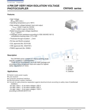
5. Mechanical and Package Information
The CNY64S uses a 4-pin DIP (Dual In-line Package). The key mechanical feature for safety is the through-insulation distance, which is guaranteed to be ≥3mm. This physical separation between the input (pins 1 & 2) and output (pins 3 & 4) sides of the package is a fundamental requirement for achieving reinforced isolation ratings at high voltages.
Pinout:
- Anode of the infrared LED
- Cathode of the infrared LED
- Emitter of the phototransistor
- Collector of the phototransistor
The package drawing (implied in the PDF) would provide exact dimensions for PCB footprint planning, including lead spacing, body width, and overall height. A recommended pad layout for surface mounting (likely for a DIP package intended for through-hole mounting but with leads formed for surface mounting) is also provided to ensure reliable solder joints and proper mechanical strength during the assembly process.
6. Soldering and Assembly Guidelines
The device can withstand a maximum soldering temperature of 260°C for a duration of less than 10 seconds, measured 2mm from the package body. This is compatible with standard lead-free reflow and wave soldering profiles. Care must be taken to avoid excessive thermal stress, which could damage the internal wire bonds or the plastic package material, potentially compromising the isolation integrity. Standard industry practices for handling moisture-sensitive devices (if applicable) should be followed. The storage temperature range is -55°C to +100°C.
7. Ordering and Packaging Information
The part number structure is: CNY64SX-V
- CNY64S: Base part number for the series.
- X: CTR rank option: 'A', 'B', or blank for the standard grade.
- -V: Optional suffix denoting VDE safety certification.
Packaging Options:
- CNY64S / CNY64S-V: Packaged in tubes containing 60 units each.
- CNY64S(TA): Packaged in tubes containing 500 units each (likely a bulk packaging option).
Device Marking: The top of the package is marked with several lines of text:
- EL: Manufacturer code.
- CNY64: Base part number.
- R: A single character representing the CTR rank (e.g., 'A' or 'B').
- Y: A one-digit code for the year of manufacture.
- WW: A two-digit code for the week of manufacture.
- V: An optional marking indicating VDE certification.
8. Application Recommendations
8.1 Typical Application Circuits
The CNY64S is versatile and can be used in several key configurations:
- Digital Signal Isolation: The simplest use case. A digital signal drives the LED via a current-limiting resistor. The phototransistor, connected as a switch with a pull-up resistor to VCC, recreates the inverted logic signal on the isolated side. The switching speed (max 18µs) supports data rates up to several tens of kHz.
- Switch Mode Power Supply (SMPS) Feedback: A critical application. The photocoupler is used to transfer the error voltage from the secondary (output) side of the power supply back to the primary-side PWM controller, maintaining the isolation barrier. The CTR linearity and stability over temperature are important here. The high isolation voltage is essential for safety in off-line power supplies.
- Microprocessor System Interface: Isolating digital I/O lines between a noisy industrial environment (e.g., 24V PLC inputs) and a sensitive microprocessor. The 80V BVCEO provides good margin for voltage spikes.
8.2 Design Considerations
- LED Current Limiting: Always use a series resistor to set the LED forward current (IF). Calculate the resistor value based on the supply voltage (Vsupply), the desired IF, and the LED's VF (use max value for worst-case design): R = (Vsupply - VF) / IF. Do not exceed the absolute maximum IF of 75mA.
- Phototransistor Biasing: The load resistor (RL) on the collector determines the output voltage swing, switching speed, and power consumption. A smaller RL gives faster speed but lower gain and higher current. Ensure the voltage across the phototransistor (VCE) does not exceed 80V in the off state.
- CTR Degradation: The CTR of photocouplers gradually decreases over time, especially when operated at high junction temperatures and high forward currents. For long-life designs, derate the operating IF and ensure adequate thermal management. Choose a device with an initial CTR well above the minimum required for your circuit at end-of-life.
- Noise Immunity: The low coupling capacitance (0.3 pF) provides good rejection of high-frequency common-mode noise. For extremely noisy environments, consider adding a small bypass capacitor (e.g., 0.1µF) across the input and/or output pins close to the device to filter high-frequency spikes.
9. Technical Comparison and Differentiation
Compared to standard 4-pin photocouplers with lower isolation ratings (e.g., 2500VRMS or 5000VRMS), the CNY64S's primary differentiator is its 8200VRMS/10000V peak isolation capability and formal reinforced isolation certification (VDE). This makes it not just a signal isolator but a certified safety component. Compared to higher-speed digital isolators (which use capacitive or magnetic coupling), the CNY64S is slower but offers inherently higher isolation voltage and robustness against dV/dt transients, often at a lower cost. Its combination of 80V output transistor rating, wide CTR selection, and safety approvals creates a strong value proposition for cost-sensitive yet safety-critical industrial and power applications.
10. Frequently Asked Questions (FAQ)
Q1: What is the difference between the standard CNY64S and the CNY64S-V?
A1: The "-V" variant has undergone and passed additional testing and certification by VDE for reinforced isolation according to specific safety standards (DIN EN 60747-5-5). It has a higher transient isolation voltage rating (10000V peak vs. 8200V peak). For applications requiring formal safety agency recognition, the -V version is necessary.
Q2: How do I choose between the CTR grades (Standard, A, B)?
A2: If your circuit design is tolerant of a wide variation in gain (e.g., a digital switch with plenty of margin), the standard grade is fine. If you need more consistent performance from unit to unit, especially in analog feedback loops or circuits where a specific minimum CTR is critical for functionality, choose the A or B grade. The B grade guarantees a higher minimum CTR (100%).
Q3: Can I use this for isolating AC mains voltage signals?
A3: Yes, but with important caveats. The device is rated for reinforced isolation for mains voltages up to specific limits depending on the application class (e.g., up to 600V for classes I-IV). You must ensure the creepage and clearance distances on your PCB around the device also meet the relevant safety standards for your working voltage. The photocoupler itself is only one part of the isolation system.
Q4: Why is the reverse voltage rating for the LED so low (5V)?
A4: Infrared LEDs are semiconductor diodes with a relatively low reverse breakdown voltage. Applying even a small reverse voltage beyond the rating can cause avalanche breakdown and immediate damage. Always ensure the driving circuit prevents reverse bias, or use a protection diode in parallel with the LED (cathode to anode) if reverse voltages are possible.
11. Practical Design Case Study
Scenario: Isolating a 5V digital signal from a microcontroller to control a 24V relay in an industrial cabinet. The environment is electrically noisy, and functional isolation is required to prevent ground loops from disrupting the microcontroller.
Design Steps:
- Component Selection: Choose CNY64SB for a guaranteed minimum CTR of 100%, ensuring strong drive even after aging.
- LED Driver: Microcontroller pin (5V output) drives the LED. Target IF = 10mA for good speed and margin. Using VF(max) = 2.0V, Rlimit = (5V - 2.0V) / 0.01A = 300Ω. Use a standard 330Ω resistor, resulting in IF ≈ 9mA.
- Output Circuit: The relay coil (24V, 100Ω coil resistance) is connected between the 24V supply and the collector of the phototransistor. The emitter is connected to ground. When the LED is on, the phototransistor saturates, pulling the collector low and energizing the relay. A flyback diode must be placed across the relay coil to suppress voltage spikes when the transistor turns off. The VCE(sat) of 0.3V is negligible. The 80V BVCEO provides ample protection against inductive kickback spikes that aren't fully clamped by the diode.
- PCB Layout: Maintain the ≥3mm creepage distance between the input-side traces (microcontroller, resistor) and the output-side traces (24V, relay) on the PCB, extending the internal isolation of the device. Place bypass capacitors (0.1µF) near the device's power pins on both sides.
This simple, robust circuit reliably isolates the control logic from the power stage using the CNY64S's key parameters.
12. Operating Principle
The CNY64S operates on the principle of electro-optical-electrical conversion. An electrical current applied to the input side flows through the infrared LED, causing it to emit light photons with a wavelength typically around 940nm. This light travels across a transparent insulating gap within the plastic package. On the output side, the light strikes the base region of the silicon NPN phototransistor, generating electron-hole pairs. This photogenerated current acts as a base current, which is then amplified by the transistor's gain (hFE), resulting in a much larger collector current. The key point is that the only connection between the input and output is the beam of light; there is no electrical conductor, thus providing galvanic isolation. The degree of isolation is determined by the optical path's physical distance and the dielectric properties of the intervening materials.
13. Technology Trends
Photocoupler technology continues to evolve. While the basic principle remains, trends include:
- Higher Integration: Combining the photocoupler with additional circuitry like Schmitt triggers, gate drivers, or I²C isolators into single packages.
- Improved Speed: Development of faster phototransistors and integrated designs for digital isolation competing in the Mbps range.
- Enhanced Reliability and Miniaturization: Improvements in LED efficiency and packaging materials to extend lifetime, reduce CTR degradation, and allow for smaller surface-mount packages (like SO-4, SO-6) while maintaining high isolation ratings.
- Focus on Safety Standards: Increasing demand for components with pre-certified reinforced isolation to simplify end-product compliance with stringent global safety regulations for medical, automotive, and industrial equipment.
LED Specification Terminology
Complete explanation of LED technical terms
Photoelectric Performance
| Term | Unit/Representation | Simple Explanation | Why Important |
|---|---|---|---|
| Luminous Efficacy | lm/W (lumens per watt) | Light output per watt of electricity, higher means more energy efficient. | Directly determines energy efficiency grade and electricity cost. |
| Luminous Flux | lm (lumens) | Total light emitted by source, commonly called "brightness". | Determines if the light is bright enough. |
| Viewing Angle | ° (degrees), e.g., 120° | Angle where light intensity drops to half, determines beam width. | Affects illumination range and uniformity. |
| CCT (Color Temperature) | K (Kelvin), e.g., 2700K/6500K | Warmth/coolness of light, lower values yellowish/warm, higher whitish/cool. | Determines lighting atmosphere and suitable scenarios. |
| CRI / Ra | Unitless, 0–100 | Ability to render object colors accurately, Ra≥80 is good. | Affects color authenticity, used in high-demand places like malls, museums. |
| SDCM | MacAdam ellipse steps, e.g., "5-step" | Color consistency metric, smaller steps mean more consistent color. | Ensures uniform color across same batch of LEDs. |
| Dominant Wavelength | nm (nanometers), e.g., 620nm (red) | Wavelength corresponding to color of colored LEDs. | Determines hue of red, yellow, green monochrome LEDs. |
| Spectral Distribution | Wavelength vs intensity curve | Shows intensity distribution across wavelengths. | Affects color rendering and quality. |
Electrical Parameters
| Term | Symbol | Simple Explanation | Design Considerations |
|---|---|---|---|
| Forward Voltage | Vf | Minimum voltage to turn on LED, like "starting threshold". | Driver voltage must be ≥Vf, voltages add up for series LEDs. |
| Forward Current | If | Current value for normal LED operation. | Usually constant current drive, current determines brightness & lifespan. |
| Max Pulse Current | Ifp | Peak current tolerable for short periods, used for dimming or flashing. | Pulse width & duty cycle must be strictly controlled to avoid damage. |
| Reverse Voltage | Vr | Max reverse voltage LED can withstand, beyond may cause breakdown. | Circuit must prevent reverse connection or voltage spikes. |
| Thermal Resistance | Rth (°C/W) | Resistance to heat transfer from chip to solder, lower is better. | High thermal resistance requires stronger heat dissipation. |
| ESD Immunity | V (HBM), e.g., 1000V | Ability to withstand electrostatic discharge, higher means less vulnerable. | Anti-static measures needed in production, especially for sensitive LEDs. |
Thermal Management & Reliability
| Term | Key Metric | Simple Explanation | Impact |
|---|---|---|---|
| Junction Temperature | Tj (°C) | Actual operating temperature inside LED chip. | Every 10°C reduction may double lifespan; too high causes light decay, color shift. |
| Lumen Depreciation | L70 / L80 (hours) | Time for brightness to drop to 70% or 80% of initial. | Directly defines LED "service life". |
| Lumen Maintenance | % (e.g., 70%) | Percentage of brightness retained after time. | Indicates brightness retention over long-term use. |
| Color Shift | Δu′v′ or MacAdam ellipse | Degree of color change during use. | Affects color consistency in lighting scenes. |
| Thermal Aging | Material degradation | Deterioration due to long-term high temperature. | May cause brightness drop, color change, or open-circuit failure. |
Packaging & Materials
| Term | Common Types | Simple Explanation | Features & Applications |
|---|---|---|---|
| Package Type | EMC, PPA, Ceramic | Housing material protecting chip, providing optical/thermal interface. | EMC: good heat resistance, low cost; Ceramic: better heat dissipation, longer life. |
| Chip Structure | Front, Flip Chip | Chip electrode arrangement. | Flip chip: better heat dissipation, higher efficacy, for high-power. |
| Phosphor Coating | YAG, Silicate, Nitride | Covers blue chip, converts some to yellow/red, mixes to white. | Different phosphors affect efficacy, CCT, and CRI. |
| Lens/Optics | Flat, Microlens, TIR | Optical structure on surface controlling light distribution. | Determines viewing angle and light distribution curve. |
Quality Control & Binning
| Term | Binning Content | Simple Explanation | Purpose |
|---|---|---|---|
| Luminous Flux Bin | Code e.g., 2G, 2H | Grouped by brightness, each group has min/max lumen values. | Ensures uniform brightness in same batch. |
| Voltage Bin | Code e.g., 6W, 6X | Grouped by forward voltage range. | Facilitates driver matching, improves system efficiency. |
| Color Bin | 5-step MacAdam ellipse | Grouped by color coordinates, ensuring tight range. | Guarantees color consistency, avoids uneven color within fixture. |
| CCT Bin | 2700K, 3000K etc. | Grouped by CCT, each has corresponding coordinate range. | Meets different scene CCT requirements. |
Testing & Certification
| Term | Standard/Test | Simple Explanation | Significance |
|---|---|---|---|
| LM-80 | Lumen maintenance test | Long-term lighting at constant temperature, recording brightness decay. | Used to estimate LED life (with TM-21). |
| TM-21 | Life estimation standard | Estimates life under actual conditions based on LM-80 data. | Provides scientific life prediction. |
| IESNA | Illuminating Engineering Society | Covers optical, electrical, thermal test methods. | Industry-recognized test basis. |
| RoHS / REACH | Environmental certification | Ensures no harmful substances (lead, mercury). | Market access requirement internationally. |
| ENERGY STAR / DLC | Energy efficiency certification | Energy efficiency and performance certification for lighting. | Used in government procurement, subsidy programs, enhances competitiveness. |