Table of Contents
- 1. Product Overview
- 1.1 Core Advantages and Target Market
- 2. Technical Parameter Deep-Dive
- 2.1 Absolute Maximum Ratings
- 2.2 Electro-Optical Characteristics
- 3. Grading System Explanation
- 4. Performance Curve Analysis
- 5. Mechanical and Package Information
- 5.1 Pin Configuration and Package Types
- 5.2 Pad Layout and Polarity
- 6. Soldering and Assembly Guidelines
- 7. Packaging and Ordering Information
- 8. Application Recommendations
- 8.1 Typical Application Scenarios
- 8.2 Design Considerations
- 9. Technical Comparison and Differentiation
- 10. Frequently Asked Questions (Based on Technical Parameters)
- 11. Practical Design and Usage Examples
- 12. Operating Principle
- 13. Technology Trends
- LED Specification Terminology
- Photoelectric Performance
- Electrical Parameters
- Thermal Management & Reliability
- Packaging & Materials
- Quality Control & Binning
- Testing & Certification
1. Product Overview
The EL817H-G series represents a family of compact, high-performance phototransistor photocouplers (optocouplers) designed for reliable signal isolation and transmission between circuits of different potentials. Each device integrates an infrared emitting diode optically coupled to a silicon phototransistor detector, housed in a standard 4-pin Dual In-line Package (DIP). The series is characterized by its high isolation capability, wide operating temperature range, and compliance with stringent environmental and safety standards, making it suitable for industrial and consumer applications.
1.1 Core Advantages and Target Market
The primary advantages of the EL817H-G series include its high isolation voltage of 5000Vrms, which ensures robust protection against voltage transients and noise. The devices are halogen-free, adhering to strict environmental regulations (Br < 900ppm, Cl < 900ppm, Br+Cl < 1500ppm). With a wide Current Transfer Ratio (CTR) range from 50% to 400% and an operating temperature range of -55°C to +125°C, these photocouplers offer design flexibility and reliability in harsh conditions. The target markets include industrial automation (Programmable Logic Controllers), telecommunications equipment, system appliances, measuring instruments, and various home appliances such as fan heaters, where safe signal transmission is critical.
2. Technical Parameter Deep-Dive
This section provides an objective and detailed analysis of the device's electrical, optical, and thermal characteristics as defined in the datasheet.
2.1 Absolute Maximum Ratings
Stresses beyond these limits may cause permanent damage. Key ratings include: Forward Current (IF) of 50mA, Peak Forward Current (IFP) of 1A for 1µs pulse, Collector-Emitter Voltage (VCEO) of 80V, and Total Power Dissipation (PTOT) of 200mW. The device can withstand an Isolation Voltage (VISO) of 5000Vrms for 1 minute under specified humidity conditions. The maximum soldering temperature is 260°C for 10 seconds.
2.2 Electro-Optical Characteristics
Detailed performance parameters are specified at Ta=25°C. The input diode has a typical Forward Voltage (VF) of 1.2V at IF=10mA. The output phototransistor's Collector-Emitter dark current (ICEO) is a maximum of 200nA at VCE=48V. The key transfer parameter, Current Transfer Ratio (CTR), is defined as the ratio of output collector current to input forward current. The EL817H-G series is offered in multiple CTR grades: EL817H (50-400%), EL817HA (80-160%), EL817HB (130-260%), and EL817HC (200-400%), all measured at IF=5mA, VCE=5V. Switching performance is characterized by Rise Time (tr) and Fall Time (tf) of 6µs and 8µs typical, respectively, under specific test conditions (VCE=2V, IC=2mA, RL=100Ω).
3. Grading System Explanation
The primary grading for this photocoupler series is based on the Current Transfer Ratio (CTR). This parameter is crucial for design as it determines the current gain of the isolation stage. Designers must select the appropriate grade (H, HA, HB, HC) based on the required sensitivity and the desired output current level for a given input current. This binning ensures consistent performance within specified bounds for different application needs, from general-purpose isolation (wider CTR range) to circuits requiring tighter gain tolerances.
4. Performance Curve Analysis
The datasheet references typical electro-optical characteristic curves. While specific graphs are not reproduced in the provided text, such curves typically illustrate the relationship between CTR and forward current (IF) at various temperatures, the dependence of forward voltage (VF) on IF, and the saturation voltage (VCE(sat)) versus collector current (IC). These curves are essential for understanding device behavior under non-standard conditions, such as high temperature or varying drive currents, allowing designers to optimize circuit performance and ensure reliability across the operating range.
5. Mechanical and Package Information
The EL817H-G is available in several 4-pin DIP package variants to suit different assembly processes.
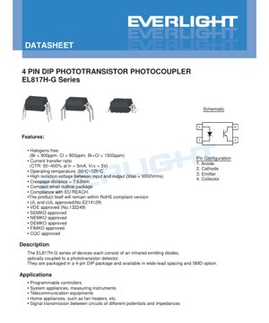
5.1 Pin Configuration and Package Types
The standard pinout is: Pin 1 (Anode), Pin 2 (Cathode), Pin 3 (Emitter), Pin 4 (Collector). The package options include: Standard DIP (through-hole), Option M (Wide lead bend with 0.4-inch/10.16mm spacing for increased creepage), Option S1 (Surface mount lead form, low profile, for tape and reel), and Option S2 (Surface mount lead form, low profile, with different body dimensions for tape and reel). Detailed dimensioned drawings for each type are provided in the datasheet, specifying critical measurements like body size, lead width, pitch, and standoff height.
5.2 Pad Layout and Polarity
For the surface-mount options (S1 and S2), the datasheet includes recommended pad layout diagrams. These diagrams suggest land pattern dimensions for PCB design to ensure proper soldering and mechanical stability. The device marking typically includes a part number code and possibly a lot identifier. The package has a notch or a dot near pin 1 for correct polarity orientation during assembly.
6. Soldering and Assembly Guidelines
The absolute maximum rating specifies a soldering temperature of 260°C for 10 seconds. For wave or reflow soldering, standard profiles for leaded packages should be followed, ensuring the peak temperature and time above liquidus do not exceed the device's limits. For the surface-mount variants, a standard infrared or convection reflow profile is applicable. It is critical to avoid excessive mechanical stress on the leads and the epoxy body. Devices should be stored in conditions within the storage temperature range of -55°C to 150°C and in moisture-sensitive packaging if applicable.
7. Packaging and Ordering Information
The part number follows the structure: EL817HX(Y)(Z)-VG. Where: H denotes high-temperature operation, X is the lead form (S1, S2, M, or none for standard), Y is the CTR rank (A, B, C, or none for the base H grade), Z is the tape and reel option (TU, TD, or none), V indicates VDE safety approval (optional), and G signifies halogen-free. Packing quantities vary: 100 units per tube for through-hole options, and 1500 or 2000 units per reel for the S1 and S2 tape & reel options, respectively.
8. Application Recommendations
8.1 Typical Application Scenarios
The EL817H-G is ideal for: Signal Isolation in PLC I/O Modules: Isolating digital signals between the low-voltage logic side and higher-voltage field side. Telecom Line Interface Cards: Providing galvanic isolation for signal or control lines. Power Supply Feedback Loops: Isolating the feedback signal from the secondary side to the primary side controller in switch-mode power supplies (SMPS). Appliance Control: Isolating user interface microcontrollers from mains-powered triac or relay drivers in devices like heaters.
8.2 Design Considerations
Current Limiting Resistor: An external resistor must be connected in series with the input LED to set the forward current (IF), typically between 5mA and 20mA for optimal CTR and speed. Load Resistor: The output collector requires a pull-up resistor (RL) to VCC to define the output logic levels and switching speed. A smaller RL gives faster switching but higher power consumption. CTR Degradation: CTR can decrease over time, especially at high operating temperatures and currents. Design should include a margin (e.g., 20-30%) to ensure circuit functionality over the product's lifetime. Noise Immunity: For noisy environments, bypass capacitors near the device and proper PCB layout (minimizing loop areas) are recommended.
9. Technical Comparison and Differentiation
Compared to basic photocouplers, the EL817H-G series differentiates itself with its high isolation voltage (5000Vrms) and creepage distance > 7.62mm, which are critical for safety-approved designs in mains-connected equipment. The halogen-free construction addresses environmental regulations like RoHS and REACH more comprehensively. The availability of multiple CTR grades and package options (DIP and SMD) provides greater design flexibility than single-variant parts. The collective safety approvals (UL, cUL, VDE, SEMKO, NEMKO, DEMKO, FIMKO, CQC) streamline the certification process for end products targeting global markets.
10. Frequently Asked Questions (Based on Technical Parameters)
Q1: What is the purpose of the different CTR grades (A, B, C)?
A1: They allow designers to select a device with a guaranteed CTR range that matches their circuit's sensitivity requirements. A tighter range (like HA, HB, HC) ensures more consistent gain from unit to unit, which is important for analog signal transmission or circuits with precise threshold levels.
Q2: Can I use this photocoupler to directly drive a relay?
A2: No, not directly. The maximum collector current (IC) is 50mA, and the saturation voltage can be up to 0.35V. Most relays require more current. The phototransistor output should be used to drive a secondary transistor or a MOSFET gate for higher current switching.
Q3: How do I choose between the Standard DIP and the SMD options?
A3: The choice depends on your assembly process. Standard DIP is for through-hole PCB assembly. Options S1 and S2 are for surface-mount assembly, which is standard for automated, high-volume production. Option M (wide lead) is a through-hole variant that offers increased creepage distance for enhanced high-voltage safety.
Q4: What does the \"-G\" suffix mean in the part number?
A4: The \"-G\" suffix indicates that the device is manufactured with halogen-free materials, complying with specific limits for bromine (Br) and chlorine (Cl) content.
11. Practical Design and Usage Examples
Example 1: Isolated Digital Input for Microcontroller. The photocoupler can interface a 24V industrial sensor signal to a 3.3V microcontroller GPIO. The sensor output drives the LED via a current-limiting resistor. The phototransistor collector is connected to the microcontroller pin (with internal pull-up enabled) and VCC (3.3V). The emitter is grounded. This provides complete galvanic isolation, protecting the MCU from voltage spikes on the sensor line.
Example 2: Feedback in a Flyback Power Supply. An error amplifier on the secondary side drives the LED of the EL817H. The phototransistor on the primary side adjusts the duty cycle of the PWM controller. The 5000Vrms isolation is essential here to meet safety standards for the isolation barrier between primary (mains) and secondary (low voltage) sides.
12. Operating Principle
A photocoupler, or optocoupler, is a device that transfers electrical signals between two isolated circuits using light. In the EL817H-G, an electrical current applied to the input pins (1 and 2) causes the infrared Light Emitting Diode (LED) to emit light. This light travels across a transparent insulating gap (typically made of mold compound) and strikes the base region of the silicon phototransistor (pins 3 and 4). The incident light generates electron-hole pairs in the base, effectively acting as a base current, which allows a much larger collector-emitter current to flow. The key point is that the only connection between the input and output is optical, providing excellent electrical isolation determined by the material and distance of the gap.
13. Technology Trends
The trend in photocoupler technology is towards higher integration, faster speeds, and lower power consumption. While phototransistor-based couplers like the EL817H-G offer good general-purpose performance and high current transfer ratio, newer technologies are emerging. These include High-Speed Digital Optocouplers with logic gate outputs and speeds in the Mbps range, IGBT/MOSFET Gate Drive Optocouplers with integrated high-current output stages, and Analog Isolation Amplifiers that provide precise linear signal transmission. Furthermore, there is a continuous push for miniaturization (smaller SMD packages), enhanced reliability (longer lifetime at higher temperatures), and broader compliance with evolving global environmental and safety standards.
LED Specification Terminology
Complete explanation of LED technical terms
Photoelectric Performance
| Term | Unit/Representation | Simple Explanation | Why Important |
|---|---|---|---|
| Luminous Efficacy | lm/W (lumens per watt) | Light output per watt of electricity, higher means more energy efficient. | Directly determines energy efficiency grade and electricity cost. |
| Luminous Flux | lm (lumens) | Total light emitted by source, commonly called "brightness". | Determines if the light is bright enough. |
| Viewing Angle | ° (degrees), e.g., 120° | Angle where light intensity drops to half, determines beam width. | Affects illumination range and uniformity. |
| CCT (Color Temperature) | K (Kelvin), e.g., 2700K/6500K | Warmth/coolness of light, lower values yellowish/warm, higher whitish/cool. | Determines lighting atmosphere and suitable scenarios. |
| CRI / Ra | Unitless, 0–100 | Ability to render object colors accurately, Ra≥80 is good. | Affects color authenticity, used in high-demand places like malls, museums. |
| SDCM | MacAdam ellipse steps, e.g., "5-step" | Color consistency metric, smaller steps mean more consistent color. | Ensures uniform color across same batch of LEDs. |
| Dominant Wavelength | nm (nanometers), e.g., 620nm (red) | Wavelength corresponding to color of colored LEDs. | Determines hue of red, yellow, green monochrome LEDs. |
| Spectral Distribution | Wavelength vs intensity curve | Shows intensity distribution across wavelengths. | Affects color rendering and quality. |
Electrical Parameters
| Term | Symbol | Simple Explanation | Design Considerations |
|---|---|---|---|
| Forward Voltage | Vf | Minimum voltage to turn on LED, like "starting threshold". | Driver voltage must be ≥Vf, voltages add up for series LEDs. |
| Forward Current | If | Current value for normal LED operation. | Usually constant current drive, current determines brightness & lifespan. |
| Max Pulse Current | Ifp | Peak current tolerable for short periods, used for dimming or flashing. | Pulse width & duty cycle must be strictly controlled to avoid damage. |
| Reverse Voltage | Vr | Max reverse voltage LED can withstand, beyond may cause breakdown. | Circuit must prevent reverse connection or voltage spikes. |
| Thermal Resistance | Rth (°C/W) | Resistance to heat transfer from chip to solder, lower is better. | High thermal resistance requires stronger heat dissipation. |
| ESD Immunity | V (HBM), e.g., 1000V | Ability to withstand electrostatic discharge, higher means less vulnerable. | Anti-static measures needed in production, especially for sensitive LEDs. |
Thermal Management & Reliability
| Term | Key Metric | Simple Explanation | Impact |
|---|---|---|---|
| Junction Temperature | Tj (°C) | Actual operating temperature inside LED chip. | Every 10°C reduction may double lifespan; too high causes light decay, color shift. |
| Lumen Depreciation | L70 / L80 (hours) | Time for brightness to drop to 70% or 80% of initial. | Directly defines LED "service life". |
| Lumen Maintenance | % (e.g., 70%) | Percentage of brightness retained after time. | Indicates brightness retention over long-term use. |
| Color Shift | Δu′v′ or MacAdam ellipse | Degree of color change during use. | Affects color consistency in lighting scenes. |
| Thermal Aging | Material degradation | Deterioration due to long-term high temperature. | May cause brightness drop, color change, or open-circuit failure. |
Packaging & Materials
| Term | Common Types | Simple Explanation | Features & Applications |
|---|---|---|---|
| Package Type | EMC, PPA, Ceramic | Housing material protecting chip, providing optical/thermal interface. | EMC: good heat resistance, low cost; Ceramic: better heat dissipation, longer life. |
| Chip Structure | Front, Flip Chip | Chip electrode arrangement. | Flip chip: better heat dissipation, higher efficacy, for high-power. |
| Phosphor Coating | YAG, Silicate, Nitride | Covers blue chip, converts some to yellow/red, mixes to white. | Different phosphors affect efficacy, CCT, and CRI. |
| Lens/Optics | Flat, Microlens, TIR | Optical structure on surface controlling light distribution. | Determines viewing angle and light distribution curve. |
Quality Control & Binning
| Term | Binning Content | Simple Explanation | Purpose |
|---|---|---|---|
| Luminous Flux Bin | Code e.g., 2G, 2H | Grouped by brightness, each group has min/max lumen values. | Ensures uniform brightness in same batch. |
| Voltage Bin | Code e.g., 6W, 6X | Grouped by forward voltage range. | Facilitates driver matching, improves system efficiency. |
| Color Bin | 5-step MacAdam ellipse | Grouped by color coordinates, ensuring tight range. | Guarantees color consistency, avoids uneven color within fixture. |
| CCT Bin | 2700K, 3000K etc. | Grouped by CCT, each has corresponding coordinate range. | Meets different scene CCT requirements. |
Testing & Certification
| Term | Standard/Test | Simple Explanation | Significance |
|---|---|---|---|
| LM-80 | Lumen maintenance test | Long-term lighting at constant temperature, recording brightness decay. | Used to estimate LED life (with TM-21). |
| TM-21 | Life estimation standard | Estimates life under actual conditions based on LM-80 data. | Provides scientific life prediction. |
| IESNA | Illuminating Engineering Society | Covers optical, electrical, thermal test methods. | Industry-recognized test basis. |
| RoHS / REACH | Environmental certification | Ensures no harmful substances (lead, mercury). | Market access requirement internationally. |
| ENERGY STAR / DLC | Energy efficiency certification | Energy efficiency and performance certification for lighting. | Used in government procurement, subsidy programs, enhances competitiveness. |